Microfabricated Chip Traps for Ions111This is a chapter from the forthcoming book “Atom Chips” edited by J. Reichel and V. Vuletic (to be published by WILEY-VCH).
1 Introduction
Most chapters of this monograph focus on trapping and manipulating neutral atoms with magnetic and optical fields. In this chapter, we discuss the trapping of atomic ions. This is of current high interest because individual ions can be the physical representations of qubits for quantum information processing [1]. For recent reviews see [2, 3]. The goals are similar to those of neutral atom traps in that we wish to create microfabricated structures to trap, transport, and arrange ions in an array. Microfabrication holds the promise of forming large arrays of traps that would allow the scaling of current quantum information processing capabilities to the level needed to implement useful algorithms [4, 5, 6, 7].
There are two primary types of ion traps used in low energy atomic physics: Penning traps and Paul traps. In a Penning trap, charged particles are trapped by a combination of static electric and magnetic fields [8, 9]. In a Paul trap, a spatially varying sinusoidally oscillating electric field, typically in the radio-frequency (rf) domain, confines atomic or molecular ions in space [10]. In this review only the Paul type will be considered.
Neutral atom traps operate by a coupling between external trapping fields and atoms’ electric or magnetic moments. Trap depths of a few kelvins are common. In ion traps, an ion is trapped by a coupling between the applied electric trapping fields and the atom’s net (or overall) charge. Typical ion trap depths are 1 eV. This coupling does not depend on the ion’s internal electronic state, leaving it largely unperturbed.
We begin this chapter with an introduction to the dynamics of ions confined in Paul traps based on the pseudopotential approximation. Subsequent topics include numeric and analytic models for various Paul trap geometries, a list of considerations for practical trap design and finally an overview of microfabricated trapping structures. A discussion of future directions concludes this chapter.
2 Radio-frequency (rf) ion traps
In this section we discuss the equations of motion of a charged particle in a spatially inhomogeneous radio-frequency (rf) field based on the pseudopotential approximation model. We then present examples of suitable electrode geometries.
2.1 Motion of ions in a spatially inhomogeneous rf field
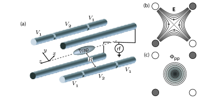
Most schemes for quantum information processing with trapped ions are based on a linear rf trap shown schematically in fig. 1a. This trap is essentially a linear quadrupole mass filter [10] with its ends plugged by static potentials [11]. The radial confinement (the - plane in fig. 1a) is provided by an rf potential applied to two of the electrodes with the other electrodes held at rf ground. In this linear geometry, the rf potential cannot generate full 3D confinement, so static potentials and applied to control electrodes provide axial ( axis) confinement. We will assume the axial trapping fields are relatively weak so that the accompanying static radial fields do not significantly perturb the radial trapping.
Applying a potential of to the rf electrodes while grounding the other electrodes (), the rf potential near the geometric center of the four rods takes the form
| (1) |
where is a distance scale that is approximately the distance from the trap axis to the nearest surface of the electrodes [10, 4, 11]. The resulting electric field is shown in fig. 1b. There is a field null at the trap center; the field magnitude increases linearly with distance from the center.
We can think of the rf electric field as analogous to the electric field from the trapping laser in an optical dipole trap [4, 12]. For a neutral atom, the laser’s electric field induces a dipole moment. If the electric field is inhomogeneous, the force on the dipole, averaged over one cycle of the radiation, can give a trapping force. For detunings red of the atom’s resonant frequency , the resulting potential is a minimum at high fields, while for detunings blue of it is a minimum at low fields. An ion, however, is a free particle in the absence of a trapping field and its eigenfrequency is zero. The rf trapping potential is therefore analogous to a blue detuned light field and the ion seeks the position of lowest intensity. In the case of eq. (1), that corresponds to .
The motion for an ion placed in this field is commonly treated in one of two ways: as an exact solution of the Mathieu differential equation or as an approximate solution of a static effective potential called the ‘pseudopotential’. The Mathieu solutions provide insights on trap stability and high frequency motion; the pseudopotential approximation is more straightforward and is convenient for the analysis of trap designs.
We define the pseudopotential that governs the secular motion as follows [13]. The motion of an ion in the rf field is a combination of fast ‘micromotion’ at the rf frequency on top of a slower ‘secular’ motion. For a particle of charge and mass in a uniform electric field , the ion motion (neglecting a drift term) takes the form
| (2) |
where is the amplitude of what we will call micromotion. If the rf field amplitude has a spatial dependence along the direction, there is a nonzero net force on the ion when we average over an rf cycle:
| (3) |
where is evaluated at what we designate as the secular position , and the pseudopotential is defined by
| (4) |
We have made the approximation that the solution in eq. (2) holds over an rf cycle and have dropped terms of higher order in the Taylor expansion of around . For regions near the center of the trapping potential, these approximations hold. In three dimensions, we make the substitution . Note that the pseudopotential depends on the magnitude of the electric field, not its direction.
For the quadrupole field given in eq. (1), the pseudopotential is that of a 2D harmonic potential (see fig. 1c):
| (5) |
where is the resonant frequency. As an example, for in a Paul trap with V, MHz and µm, which are typical parameters for a microfabricated trap, the radial oscillation frequency is MHz.
The rf pseudopotential provides confinement of the ion in the radial (-) plane. Axial trapping is obtained by the addition of the static control potentials and , as shown in fig. 1a.
For , multiple ions trapped in the same potential well will form a linear ‘crystal’ along the trap axis due to a balance between the axial trapping potential and the ions’ mutual Coulomb repulsion. The inter-ion spacing is determined by the axial frequency (). The characteristic length scale of ion-ion spacing is
| (6) |
For a three-ion crystal the adjacent separation of the ions is [4]. For example, µm for and MHz. For multiple ions in a linear Paul trap, is the frequency of the lowest vibrational mode (the center of mass mode) along the trap axis.
A single ion’s radial motion in the potential given by eq. (5) can be decomposed into uncoupled harmonic motion in the and directions, both with the same trap frequency . Because the potential is cylindrically symmetric about , we could choose the decomposition about any two orthogonal directions, called the principle axes. We will see in section 3.1 when discussing Doppler cooling that we need to break this cylindrical symmetry by the application of static electric fields. In that case, the choice of the principle axes becomes fixed with corresponding radial trapping frequencies and , one for each principle axis.
2.2 Electrode geometries for linear quadrupole traps
Designs for miniaturized ion traps conserve the basic features of the Paul trap shown in fig. 1. Figure 2 shows a few geometries that have been experimentally realized. All these geometries generate a radial quadratic potential near the trap axis, though the extent of deviations from the ideal quadrupole potential away from the axis will depend on the design.
In one particular geometry, the electrodes all lie in a single plane, as shown in fig. 2d with the ion suspended above the plane [14, 15, 16, 17, 18, 19, 20]. Trapping in such surface electrode (SE) traps is possible over a wide range of geometries, albeit with to the motional frequencies and to the trap depth of more conventional quadrupolar geometries at comparable rf potentials and ion-electrode distances [14].
Advantages of the SE trap geometry over the other geometries shown in fig. 2 include easier fabrication and the possibility of integrating control electronics on the same trap wafer [6]. A SE trap at cryogenic temperature was demonstrated at MIT in 2008 [19].

Research on SE trap designs is ongoing and holds promise to yield complex geometries that would be difficult to realize in non-surface electrode designs.
3 Design considerations for Paul traps
In this section, we will discuss the requirements that need to be addressed when designing a practical ion trap.
3.1 Doppler cooling
For Doppler laser cooling of an ion in a trap, only a single laser beam is needed; trap strengths far exceed the laser beam radiation pressure. The cooling is offset by heating from photon recoil. Therefore, to cool in all directions, the Doppler cooling beam k-vector must have a component along all three principal axes of the trap [28]. This also implies that the trap frequencies are not degenerate, otherwise one principal axis could be chosen normal to the laser beam’s k-vector.
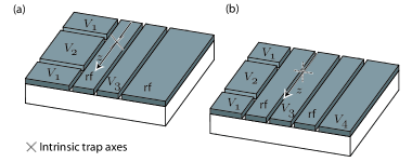
Meeting the first condition is usually straightforward for non-SE type traps, where access for the laser beam is fairly open (see fig. 3). For SE traps, where laser beams are typically constrained to run parallel to the chip surface, care has to be taken in designing the trap so that neither radial principle axis is perpendicular to the trap surface. Alternately, for SE traps, we could bring the Doppler laser beam at an angle to the surface but the beam would have to strike the surface. This can cause problems with scattered light affecting detection of the ion and with charging of exposed dielectrics (see section 3.3).

If any two trap frequencies are degenerate, then the trap axes in the plane containing those modes are not well defined and the motion in a direction perpendicular to the Doppler laser beam k-vector will not be cooled and will be heated due to photon recoil. The axial trap frequency can be set independently of the radial frequencies and can be chosen to prevent a degeneracy with either of the radial modes. However, the two radial modes could still be degenerate. There are several ways to break this degeneracy, but usually the axial trapping potential is sufficient. When we apply an axial trapping potential, Laplace’s equation forces us to have a radial component to the electric field. In general, this radial field is not cylindrically symmetric about and will distort the net trapping potential, as shown in fig. 4, thereby lifting the degeneracy of the radial frequencies. If this is not sufficient, offsetting all the control electrodes by a common potential with respect to the rf electrodes will result in a static field that has the same spatial dependence (that is the same function of and ) as the field generated by the rf electrodes. This field, shown in fig. 1b, can be used to split the radial frequencies. We will refer to the axes’ orientation resulting from the offset of all control electrodes as the ‘intrinsic’ trap axes since it does not depend on the segmentation of the control electrodes, but only on the overall geometry of the rf and control electrodes. The static axial potential might or might not define trap axes aligned with the intrinsic axes, but, overall, the control electrodes and axial potential can be configured to prevent either radial modes from being normal to the surface in an SE trap. Furthermore, in some cases additional control electrodes are designed into the trap to lift the degeneracy independent of both the axial potential and the intrinsic axes.

3.2 Micromotion
If the pseudopotential at the equilibrium position of a trapped ion is nonzero, then the ion motion will include a persistent micromotion component at frequency . There are two mechanisms that can generate a nonzero equilibrium pseudopotential. As the trapping structures become more complicated and the symmetry of the simple Paul trap in fig. 1 is broken, there can be a component of the rf field in the axial direction at the pseudopotential minimum; that is, the pseudopotential minimum need not be a pseudopotential zero. Since this effect is caused by the geometry of the trap, we refer to the resulting micromotion as ‘intrinsic’ micromotion [29]. Secondly, if there is a static electric field at the pseudopotential zero, the equilibrium position of an ion will be shifted away from the pseudopotential minimum. Because shim potentials can be applied to the control electrodes to null these fields [29], the micromotion due to this mechanism is called ‘excess’ micromotion.
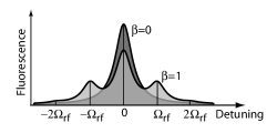
Both intrinsic and excess micromotion can cause problems with the laser-ion interactions, such as Doppler cooling, ion fluorescence, and Raman transitions [4, 29]. An ion with micromotion experiences a frequency-modulated laser field due to the Doppler shift. In the rest frame of the ion, this modulation introduces sidebands to the laser frequency (as seen by the ion) at integer multiples of and reduces the laser beam’s intensity at the carrier frequency, as shown in fig. 5. The strength of these sidebands is parametrized by the modulation index , given by
| (7) |
where is the micromotion amplitude, is the laser wavelength, and is the angle the laser beam k-vector makes with the micromotion. For laser beams tuned near resonance, ion fluorescence becomes weaker and can disappear entirely. As another example, when , the carrier and first micromotion sideband have equal strength. For , the fractional loss of on-resonance fluorescence is approximately . As a rule of thumb, we aim for , which corresponds to a drop of less than five percent in on-resonant fluorescence.
For a given static electric field in the radial plane, an ion’s radial displacement from the trap center and the resulting excess micromotion amplitude are
| (8) |
where is the radial trapping frequency.
Assume , MHz and MHz. A typical SE trap with µm and an excess potential of 1 V on a control electrode will produce a radial electric field at the ion of V/m. The resulting displacement is nm and the corresponding micromotion amplitude is nm. This results in a laser modulation index of .
Stray electric fields can be nulled if the control electrode geometry permits application of independent compensation fields along each radial principle axis. For the Paul trap in fig. 1, a common potential applied to the control electrodes can only generate a field at the trap center that is along the diagonal connecting the electrodes. We can compensate for other directions by applying, for example, a static potential offset to one of the rf electrodes or by adding extra compensation electrodes.
There are several experimental approaches to detecting and minimizing excess micromotion [29]. One technique uses the dependence of the fluorescence from a cooling laser beam on the micromotion modulation index. The micromotion can be minimized by maximizing the fluorescence when the laser is near resonance and minimizing the fluorescence when tuned to the rf sidebands.
Intrinsic micromotion can also be caused by an rf phase difference between the two rf electrodes. A phase difference can arise due to a path length difference or a differential capacitive coupling to ground for the leads supplying the electrodes with rf potential [29, 20]. We aim for (see section 3.2) for typical parameters, which requires .
3.3 Exposed dielectrics
Exposed dielectric surfaces near the trapping region can pose a problem due to charging of these surfaces and resulting stray electric fields. Charging can be caused by photo-emission by the probe laser or from electron sources such as those used for loading ions into the traps. Depending on the resistivity of the dielectric, these charges can remain on the surfaces for minutes or longer, requiring time-dependent micromotion nulling or waiting a sufficient time for the charge to dissipate.
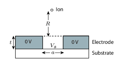
Surface electrode traps can be particularly prone to this problem. The metallic trapping electrodes are often supported by an insulating substrate and the spaces between the electrodes expose the substrate. The effect of charging these regions can be mitigated by increasing the ratio of electrode conductor thickness to the inter-electrode spacing.
Figure 6 illustrates a model for estimating how thick electrodes can suppress the field from a strip of exposed substrate charged to a potential . The sidewalls are assumed conducting and grounded. Along the midpoint of the trench the potential drops exponentially with height [30]. Using this solution to relate to the potential at the top of the trench, and employing the techniques described in section 6.2 to relate the surface potential to a field at the ions, we obtain an approximate expression for the field seen by the ion:
| (9) |
where is the width of the exposed strip of substrate, is the electrode thickness, is the distance from the trap surface to the ion, and we have assumed . Thus, the effect of the stray charges drops off rapidly with the ratio of electrode thickness to gap spacing.
3.4 Loading ions
Ions are loaded into traps by ionizing neutral atoms as they pass through the trapping region. The neutral atoms are usually supplied by a heated oven but can also come from background vapor in the vacuum or laser ablation of a sample.
It is necessary that the neutral atom flux reach the trapping region but not deposit on insulating spacers, which might cause shorting between adjacent trap electrodes. In practice, this is accomplished by careful shielding and, in some SE traps, undercutting of electrodes to form a shadow mask (see fig. 18). Alternately, for SE traps, a hole machined through the substrate can be used to direct neutral flux from an oven on the back side of the wafer to a small region of the trap, preventing coating of the surface. This is called backside loading and has been demonstrated in several traps (see section 7).
3.5 Electrical connections
The control potentials and rf trapping potentials are delivered to the trap electrodes by wiring that includes conducting traces on the trap substrate. Care is needed to avoid several pitfalls.
The high-voltage rf potential is typically produced with resonant rf transformers [31, 32, 33]. Rf losses in a microtrap’s electrodes or insulating substrate can degrade the resonator (loaded) quality factor () and can cause ohmic heating of the microtrap itself. This can be be mitigated by use of low-loss insulators (for example, quartz or alumina) and decreasing the capacitive coupling of the rf electrodes to ground through the insulators. Typical rf parameters are to 100 MHz, and .
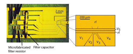
The rf electrodes have a small capacitive coupling to each control electrode (typically less than pF), which can result in rf potential on the control electrodes. This rf potential needs to be shunted to ground by a capacitor as shown in fig. 7. A low-pass RC filter (typically and ) on each control electrode is used to filter noise introduced by the externally-applied control electrode potentials. The impedance of the lines between the control electrodes and should be low or the rf shunting to ground will be compromised. Proper grounding, shielding and filtering of the electronics supplying the control electrode potentials are also important to suppress pickup and ground loops (which can cause motional heating; see section 3.6).

3.6 Motional heating
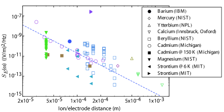
Doppler and Raman cooling can place a trapped ion’s harmonic motion into the ground state with high probability [4, 34, 35, 36]. If we are to use the internal states of an ion to store information, we must turn off the cooling laser beams during that period. Unfortunately, the ions do not remain in the motional ground state and this heating can reduce the fidelity of operations performed with the ions. One source of heating comes from laser interactions used to manipulate the electronic states [37]. Another source is ambient electric fields that have a frequency component at the ion’s motional frequencies. We expect such fields from the Johnson noise on the electrodes [4, 38, 39, 40], but the heating rates observed experimentally are typically several orders of magnitude larger than the Johnson noise can account for. Currently, the source of this anomalous heating is not explained, but recent experiments [39, 19] indicate it is thermally activated and consistent with patches of fluctuating potentials with a size scale smaller than the ion-electrode spacing [38].
The spectral density of electric field fluctuations at the ion’s position inferred from ion heating measurements in a number of traps is plotted versus the minimum ion-electrode separation in fig. 8. The dependence of on and on the trap frequency follows a roughly scaling, where [38, 39] and to 1.4 [38, 39, 16, 19]. In addition to being too small to account for these measured heating rates, Johnson noise scales as [4, 38]. One candidate mechanism that does scale as is noise caused by small fluctuating patch potentials on the electrode surfaces [38]. The potentials on these patches fluctuate at megahertz frequencies and generate a corresponding fluctuating electric field at the ion’s equilibrium position. This field can lead to heating of the ion [41, 42, 43, 38, 39, 40].
In the context of ion quantum information processing, microtraps are advantageous because quantum logic gate speeds and ion packing densities increase as the trap size decreases [4, 5, 44, 6]. However, these gains are at odds with the highly unfavorable dependence of motional heating on ion-electrode distance. For example, extrapolating from the room temperature heating results of [16], a µm trap might exceed quanta per second. Heating between gate operations can also be problematic because hot ions require more time to recool to the motional ground state.
4 Measuring heating rates
Heating rates have often been measured by observing an ion’s energy increase after cooling to the motional ground state, a relatively complicated and technically challenging undertaking [34, 35]. This section outlines a method to measure ion motional heating with a single low power laser beam [50, 51, 23]. Near resonance, an atom’s fluorescence rate is influenced by its motion due to the Doppler effect. This can be exploited in the following way:
-
1.
Cool a trapped ion to its Doppler limit.
-
2.
Let it remain in the dark for some time. Ambient electric fields couple to the ion’s motion and heat it.
-
3.
Turn on the Doppler cooling laser and measure the ion’s time-resolved fluorescence, as shown in fig. 9.
-
4.
A fit to a theoretical model of the ion fluorescence rate versus time (during recooling) [51] gives an estimate of the ion’s temperature at the end of step 2.
The theoretical model in [51] explored cooling of hot ions where the average modulus of the Doppler shift is on the order of, or greater than, the cooling transition line width . The model is a one-dimensional semiclassical theory of Doppler cooling in the weak binding limit where . It is assumed that hot ions undergo harmonic oscillations with amplitudes corresponding to the Maxwell-Boltzman energy distribution when averaged over many experiments.
As a one-dimensional (1D) model, only a single motional mode is assumed to be hot. Since the electric field spectral density at the ion is observed to scale approximately as , where to 1.4 [38, 39, 16, 19], the heating is effectively 1D if . This is also important experimentally because efficient Doppler cooling requires laser beam overlap with all modes simultaneously: a change in ion fluorescence can arise from heating of any mode.
Heating rates measured with the recooling technique were found to be in reasonable agreement with rates measured starting from the ground state and allowing heating to only a few average motional quanta [34, 35]. In these comparisons, heating seems to be approximately linear from the ground state to at least 10000 motional quanta. The disadvantage of the recooling technique is that for small heating rates, the duration of step 2 can become quite long.

5 Multiple trapping zones
Much of the emphasis in the recent generation of ion traps is towards traps that can store ions in multiple trapping zones and can transport ions between the zones.
We can modify the basic Paul trap in fig. 1 to support multiple zones and ion transport by dividing the control electrodes into a series of segments as shown in fig. 10a. By applying appropriate potentials [21, 52, 22, 53, 54, 55, 56, 23] to these segments, an axial harmonic well can be moved along the length of the trap carrying ions along with it (fig. 10b). In the adiabatic limit (with respect to ), ions have been transported a distance of 1.2 mm in 50 µs with undetectable heating or internal-state decoherence [21].
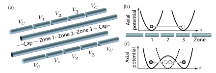
As an example relevant to quantum information processing, we need to be able to take pairs of ions in a single zone (for example, zone 2 in fig. 10c) and separate them into independent zones (one ion in zone 1 and a second in zone 3) without excessive heating. Likewise, we need to reverse this process and combine the ions into a single well. Separating and recombining are more difficult tasks than ion transport; the theory is discussed in [53] and experimentally demonstrated in [21, 52]. The basis for these potentials is the quadratic and quartic terms of the axial potential. Proper design of the trap electrodes can increase the strength of the quartic term and facilitate faster ion separation and merging with less heating. Groups of two and three ions have been separated while heating the center of mass mode to less than 10 quanta and the higher order modes to less than 2 quanta [52].
The segmented Paul trap in fig. 10 forms a linear series of trapping zones, but other geometries are desirable. Of particular interest are junctions with linear trapping regions extending from each leg. Specific junction geometries are discussed in section 7. The broad goal is to create large interconnected trapping structures that can store, transport and reorder ions so that any two ions can be brought together in a common zone [4, 5].
6 Trap modeling
Calculation of trap depth, secular frequencies, and transport and separation waveforms requires detailed knowledge of the potential and electric fields near the trap axis. In the pseudopotential approximation, the general time-dependent problem is simplified to a slowly varying electrostatic one. For simple four-rod type traps, good trap design is not difficult using numerical simulation owing to their symmetry. However, SE trap design is more complicated since the potential may have large anharmonic terms and highly asymmetric designs are common. Fortunately, for certain SE trap geometries, analytic solutions exist. These closed-form expressions permit efficient parametric optimization of electrode geometries not practical by numerical methods. In this section, we will first discuss the full 3D calculations and then introduce the analytic solutions.
6.1 Modeling 3D geometries
There are several numerical methods for solving the general electrostatic problem. In our trap simulations, we use the boundary element method implemented in a commercial software package. In contrast to the finite element method, the solutions from the boundary element method are in principle differentiable to all orders. A simulation consists of calculating the potential due to each control electrode when that electrode is set to a fixed non-zero potential and all others are grounded. The solution for an arbitrary set of potentials on the control electrodes is then a linear combination of these particular solutions. Similarly, the pseudopotential is obtained by scaling the field calculated for a finite potential on the rf electrodes and ground on the control electrodes and then squaring the field according to eq. (4).
6.2 Analytic solutions for surface electrode traps
Numerical calculations work for any electrode geometry, but they are are slow and not well suited to automatic optimization of SE trap electrode shapes. For the special case of SE traps, an analytic solution exists subject to a few realistic geometric constraints. Electrodes are modeled as a collection of separately biased regions embedded in an infinite ground plane (see fig. 11) without gaps between the electrodes. The electric field that would be observed from a biased region is proportional to the magnetic field produced by a current flowing along its perimeter [57]. The problem is then reduced from solving Laplace’s equation to integrating a Biot-Savart type integral around the patch boundary. Furthermore, for patches that have boundaries composed of straight line segments, the integrals have analytic solutions. The application of this technique to SE traps is given in [58].
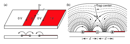
The main shortcoming of this method is the requirement that there be no gaps between the electrodes. Typical SE trap fabrication techniques produce 1 to 5 µm gaps which can only be accounted for at the level important to ion dynamics by full numerical simulations.
Fields for arbitrarily shaped patches can be calculated using this Biot-Savart technique, but for simplicity we restrict ourselves to strips that extend to infinity in the -direction of fig. 11. For this particular case, we can also derive potentials from the calculated fields. A strip extending from to with held at potential leads to a spatial potential
| (10) |
The potentials of multiple, non-overlapping strips can then be summed for more complex structures.
Two basic SE trap geometries are the ‘four-wire’ trap and the ‘five-wire’ trap. An example four-wire trap consists of an rf electrode from to and another semi-infinite rf electrode from to (see fig. 11a and fig. 16). An example five-wire trap consists of two symmetric rf electrodes from to and to . Their respective potentials are given by
| (11) |
From the electric fields and eq. (4) we can derive the pseudopotential. Note that the potential minima coincide with the points of zero electric field that lie in the line of symmetry around at and , respectively. For an ion of mass and charge , the trap frequencies along the two degenerate radial directions are
| (12) |
where is the rf-drive frequency. Figure 12 shows the general shape of the pseudopotential well along the -axis at for the four-wire trap (for the five-wire trap the potential looks very similar).
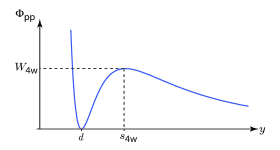
The potential is zero at where the ion is trapped, then rises to a maximum and finally asymptotically drops towards zero for . The positions of the maxima are at
| (13) |
and the pseudopotential well depth (in eV) is
| (14) |
To get an idea of practical parameters, we can calculate the radial frequency and pseudopotential well depth of a four-wire trap with a geometry similar to the trap described in [16]. For MHz, V, 40 µm and the mass of a 24Mg+ ion, we get 16.9 MHz and 203 meV.
7 Trap examples
Having covered the general principles for Paul trap designs, we now give specific examples of microfabricated ion traps. A number of fabrication techniques have been used for micro-traps, starting with assembling multiple wafers to form a traditional Paul trap type design [21, 22, 27, 23, 24, 20, 25]. Recently, trap fabrication has been extended to monolithic designs using substrate materials such as Si, GaAs, quartz, and printed circuit board [15, 16, 17, 26, 59, 18, 19, 20]. The fabrication process includes such microfabrication standards as photolithography, metalization, and chemical vapor deposition as well as other less used techniques such as laser machining.
The microfabricated equivalent to the prototypical four-rod Paul trap can use two insulating substrates patterned with electrodes that are then clamped or bonded together with an insulating spacer. This approach has been implemented in a number of traps [21, 52, 22, 20, 24, 25] using two substrates, as shown in fig. 13a. Alternatively, it is possible to build this structure into a single monolithic device [26], as indicated schematically in fig. 14a.
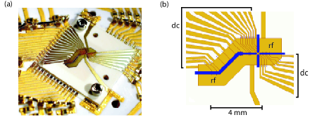
Reference [27] describes a three-wafer trap design like that shown in fig. 13b incorporating a ‘T’ shaped junction. At NIST, a two-layer trap with an ‘X’ junction has recently been implemented [25] and is shown in fig. 15. Such two-dimensional geometries will be important in order to combine arbitrarily selected qubits from an array together in the same trap zone.
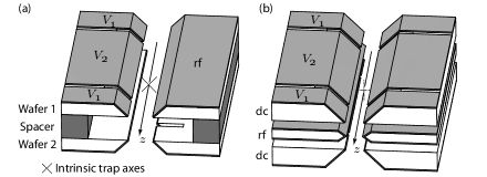
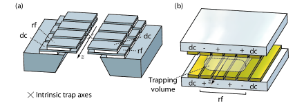
Another approach demonstrated recently used two patterned substrates, without slots, that are mounted with the conducting layers facing each other [60] (see fig. 14b). The array of conducting gold electrode strips is driven with rf that alternates between a phase of and from one strip to the next. This creates a pseudopotential that is near zero for much of the space between the wafers but which rises sharply near the substrates. When combined with static potentials at the edges of the wafers, this trap generates a near field-free region bounded by ‘hard’ potential walls (fig. 14b). Arrays of cylindrical Paul type traps have been microfabricated on silicon for use as mass spectrometers [59].
Surface electrode (SE) traps have the benefit of using standard microfabrication methods where layers of metal and insulator are deposited on the surface of the wafer without the need for milling of the substrate itself. There are two general versions of the surface trap electrode geometry, as described in section 6.2 and shown in fig. 16. The four-wire geometry has the intrinsic trap axes rotated at 45∘ to the substrate plane, which allows for efficient laser cooling of the ion. The five-wire geometry has one intrinsic trap axis perpendicular to the surface, which can make that axis difficult to Doppler cool (see section 3.1). To enable Doppler cooling, additional control electrodes can be added to the design to rotate the trap axes away from the intrinsic direction. Alternately, a hybrid between the four- and five-wire designs where the rf strips are of unequal widths (an ‘asymmetric’ five-wire trap) will rotate the intrinsic axes and enable cooling.
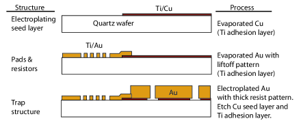
Surface electrode traps are relatively new and only a few designs have been demonstrated [15, 16, 17, 18, 19]. An SE trap was first demonstrated with charged polystyrene balls using standard PC board fabrication techniques [15]. The first SE trap for atomic ions was constructed on a fused quartz substrate with electroplated gold electrodes [16, 20]. In addition, meander-line resistors were fabricated on the chip as part of the control electrode filtering. Surface-mount capacitors were gap welded to the chip to complete the filters (see section 3.5). The fabrication process sequence is shown in fig. 18. The bonding pads and the thin meander-line resistors were formed by liftoff of evaporated gold. Charging of the exposed substrate between the electrodes was a concern, so the trap electrodes were made of 6 µm thick electroplated gold with 8 µm gaps so as to shield the ion somewhat from the charges on the quartz surface.
A similar design was built by a group at MIT for low-temperature testing using 1 µm evaporated silver on quartz [19]. They reported a strong dependence of the anomalous ion heating on temperature (see section 3.6).
The construction of the traps in [16] and [19] was based on adding conducting layers to an insulating substrate. An alternate fabrication method used boron-doped Si wafers anodically bonded to a glass substrate [17] and boron-doped silicon-on-insulator (SOI) wafers [20]. In both cases trenches were etched through the silicon layer to the glass or embedded insulating layer to define the trap electrodes. The SOI design demonstrated multiple trapping zones in a SE trap and backside loading of ions.
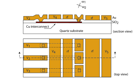
Surface electrode traps allow for complex arrangements of trapping zones, but making electrical connections to these electrodes quickly becomes intractable as the complexity grows. This problem can be addressed by incorporating multiple conducting layers into the design with only the field from the top layer affecting the ion [6, 61]. An example of such a multilayer trap fabricated on an amorphous quartz substrate at NIST is shown in fig. 19. The metal layers are separated by chemical vapor deposited (CVD) silicon dioxide and connections between metal layers are made by vias that are plasma etched through the oxide, as shown in fig. 20. The fabrication process for the surface gold layer is similar to the electroplating shown in fig. 18.
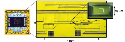
In the last three years, microfabricated traps have also been produced by Sandia National Laboratory (contact: M. Blaine, SNL) and Lucent Technologies (contact: R. Slusher, Georgia Tech Research Institute) and distributed to several ion trap groups in the framework of a "trap foundry" initiated by DTO (now IARPA). Several groups have seen trapping in the Lucent trap, a 17-zone SE trap. The Sandia trap, a 5-zone planar trap where the ions reside in-plane with the electrodes, has also been used to trap ions in two laboratories.
8 Future
As ion traps become smaller, trap complexity increases and features such as junctions promise to expand the capabilities of such traps. The two experimentally demonstrated atomic ion traps with junctions (see [27] and fig. 15) are based on multilayer designs. The slots and difficulty of alignment and bonding in multiwafer traps make it difficult to scale such structures.
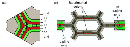
Figure 21a shows an example design of a ‘Y’ version of an SE trap junction. The shape of the rf junction is an example of the optimization that is possible with SE traps because of the efficient methods described in section 6.2 to calculate the fields. The electrode geometry has been optomized to generate a pseudopotential that has minimal axial ‘bumps’ so that rf micromotion during ion transport will be minimized (see section 3.2). Components such as this ‘Y’ could then be assembled into larger structures as shown in fig. 21b. Surface electrode traps fabricated using standard recipes in a foundry and using standard patterns may eventually make ion traps more accessible to research groups that do not have the resources needed to develop their own.
With increased trap complexity, several other issues arise. One of these is the question of how to package traps and provide all the electrical connections needed to operate them. Another issue is that of corresponding complexity of the lasers used in manipulating the ions. Beyond cooling, state preparation, and detection, lasers are needed to coherently manipulate the internal states of the ions and couple pairs or groups of ions. Multiplexing sets of lasers to address multiple trapping zones for parallel processing will be difficult. Alternatives to laser optical field state manipulation have been proposed [62, 63, 64, 65, 66] where magnetic structures, both active wire loops and passive magnetic layers, replace laser beams. If proven to be viable, this would transfer much of the experimental complexity from large laser systems to electronic packages, which can be more reliably engineered and should be scalable [6].
9 Acknowledgments
Work supported by the NIST Quantum Information Program and IARPA. This manuscript is a publication of NIST and is not subject to U.S. copyright.
References
- [1] J. I. Cirac and P. Zoller, Quantum computations with cold trapped ions, Phys. Rev. Lett. 74, 4091 (1995).
- [2] R. Blatt and D. Wineland, Entangled states of trapped atomic ions, Nature 453, 1008 (2008).
- [3] C. Monroe and M. Lukin, Remapping the quantum frontier, Physics World, Aug 32 (2008).
- [4] D. Wineland, C. Monroe, W. Itano, D. Leibfried, B. King, and D. Meekhof, Experimental issues in coherent quantum-state manipulation of trapped atomic ions, J. Res. Natl. Inst. Stand. Technol. 103, 259 (1998).
- [5] D. Kielpinski, C. Monroe, and D. Wineland, Architecture for a large-scale ion-trap quantum computer, Nature 417, 709 (2002).
- [6] J. Kim, S. Pau, Z. Ma, H. R. McLellan, J. V. Gates, A. Kornblit, R. E. Slusher, R. M. Jopson, I. Kang, and M. Dinu, System design for large-scale ion trap quantum information processor, Quant. Inf. Comp. 5, 515 (2005).
- [7] A. M. Steane, How to build a 300 bit, 1 gig-operation quantum computer, Quant. Inf. Comp. 7, 171 (2007).
- [8] F. M. Penning, Die Glimmentladung bei niedrigem Druck zwischen koaxialen Zylindern in einem axialen Magnetfeld, Physica 3, 873 (1936).
- [9] H. Dehmelt, Experiments with an isolated subatomic particle at rest, Rev. Mod. Phys. 62, 525 (1990).
- [10] W. Paul, Electromagnetic traps for charged and neutral particles, Rev. Mod. Phys. 62, 531 (1990).
- [11] D. J. Wineland and L. Houches, Quantum information processing in ion traps, In D. Estève, J.-M. Raimond, and J. Dalibard (eds.), Session LXXIX, 2003, Quantum Entanglement and Information Processing, 261–293, Elsevier, Amsterdam (2004).
- [12] R. Grimm, M. Weidemuller, and Y. B. Ovchinnikov, Optical dipole traps for neutral atoms, Adv. At., Mol., Opt. Phys. 42, 95 (2000).
- [13] H. G. Dehmelt, Radiofrequency spectroscopy of stored ions I - storage, Ad. At. Mol. Phys. 3, 53 (1967).
- [14] J. Chiaverini, R. B. Blakestad, J. Britton, J. D. Jost, C. Langer, D. Leibfried, R. Ozeri, and D. Wineland, Surface-electrode architecture for ion-trap quantum information processing, Quant. Inf. Comp. 5, 419 (2005).
- [15] C. E. Pearson, D. R. Leibrandt, W. S. Bakr, W. J. Mallard, K. R. Brown, and I. L. Chuang, Experimental investigation of planar ion traps, Phys. Rev. A 73, 032307 (2006).
- [16] S. Seidelin, J. Chiaverini, R. Reichle, J. J. Bollinger, D. Leibfried, J. Britton, J. H. Wesenberg, R. B. Blakestad, R. J. Epstein, D. B. Hume, W. M. Itano, J. D. Jost, C. Langer, R. Ozeri, N. Shiga, and D. J. Wineland, Microfabricated surface-electrode ion trap for scalable quantum information processing, Phys. Rev. Lett. 96, 253003 (2006).
- [17] J. Britton, D. Leibfried, J. Beall, R. B. Blakestad, J. J. Bollinger, J. Chiaverini, R. J. Epstein, J. D. Jost, D. Kielpinski, C. Langer, R. Ozeri, R. Reichle, S. Seidelin, N. Shiga, J. H. Wesenberg, and D. J. Wineland, A microfabricated surface-electrode ion trap in silicon (2006), arXiv:quant-ph/0605170.
- [18] K. R. Brown, R. J. Clark, J. Labaziewicz, P. Richerme, D. R. Leibrandt, and I. L. Chuang, Loading and characterization of a printed-circuit-board atomic ion trap, Phys. Rev. A 75, 015401 (2007).
- [19] J. Labaziewicz, Y. Ge, P. Antohi, D. Leibrandt, K. R. Brown, and I. L. Chuang, Suppression of heating rates in cryogenic surface-electrode ion traps, Phys. Rev. Lett. 100, 013001 (2008).
- [20] J. Britton, Microfabricated ion traps for quantum computing, Ph.D. thesis, University of Colorado, Boulder.
- [21] M. A. Rowe, A. Ben-Kish, B. DeMarco, D. Leibfried, V. Meyer, J. Beall, J. Britton, J. Hughes, W. M. Itano, B. Jelenkovic, C. Langer, T. Rosenband, and D. J. Wineland, Transport of quantum states and separation of ions in a dual rf ion trap, Quant. Inf. Comp. 2, 257 (2002).
- [22] D. J. Wineland, D. Leibfried, M. D. Barrett, A. Ben-kish, J. C. Bergquist, R. B. Blakestad, J. J. Bollinger, J. Britton, J. Chiaverini, B. Demarco, D. Hume, W. M. Itano, M. Jensen, J. D. Jost, E. Knill, J. Koelemeij, C. Langer, W. Oskay, R. Ozeri, R. Reichle, T. Rosenband, T. Schaetz, P. O. Schmidt, and S. Seidelin, Quantum control, quantum control, quantum information processing, and quantum-limited metrology with trapped ions, In E. A. Hinds, A. Ferguson, and E. Riis (eds.), Proc. XVII Int. Conf. on Laser Spectroscopy, Avemore, Scotland, 2005, 393 – 402, World Scientific, Singapore (2005), (quant-ph/0508025).
- [23] G. Huber, T. Deuschle, W. Schnitzler, R. Reichle, K. Singer, and F. Schmidt-Kaler, Transport of ions in a segmented linear Paul trap in printed-circuit-board technology, New J. Phys. 10, 013004 (2008).
- [24] S. A. Schulz, U. Poschinger, F. Ziesel, and F. Schmidt-Kaler, Sideband cooling and coherent dynamics in a microchip multi-segmented ion trap, New J. Phys. 10, 045007 (2008).
- [25] R. B. Blakestad, private communication.
- [26] D. Stick, W. K. Hensinger, S. Olmschenk, M. J. Madsen, K. Schwab, and C. Monroe, Ion trap in a semiconductor chip, Nature Phys. 2, 36 (2006).
- [27] W. K. Hensinger, S. Olmschenk, D. Stick, D. Hucul, M. Yeo, M. Acton, L. Deslauriers, C. Monroe, and J. Rabchuk, T-junction ion trap array for two-dimensional ion shuttling, storage and manipulation, App. Phys. Lett. 88, 034101 (2006).
- [28] W. M. Itano and D. J. Wineland, Laser cooling of ions stored in harmonic and Penning traps, Phys. Rev. A 25, 35 (1982).
- [29] D. J. Berkeland, J. D. Miller, J. C. Bergquist, W. M. Itano, and D. J. Wineland, Minimization of ion micromotion in a Paul trap, J. App. Phys. 83, 5025 (1998).
- [30] J. D. Jackson, Classical electrodynamics, Wiley, New York, 3rd edn. (1999).
- [31] W. W. Macalpine and R. O. Schildknecht, Coaxial resonators with helical inner conductor, Proceedings of the IRE 47, 2099 (1959).
- [32] M. Cohen, Design techniques utilizing helical line resonators, The Microwave Journal 8, 69 (1965).
- [33] S. R. Jefferts, C. Monroe, E. W. Bell, and D. J. Wineland, Coaxial-resonator-driven rf (Paul) trap for strong confinement, Phys. Rev. A 51, 3112 (1995).
- [34] F. Diedrich, J. C. Bergquist, W. M. Itano, and D. J. Wineland, Laser cooling to the zero-point energy of motion, Phys. Rev. Lett. 62, 403 (1989).
- [35] C. Monroe, D. M. Meekhof, B. E. King, S. R. Jefferts, W. M. Itano, D. J. Wineland, and P. Gould, Resolved-sideband raman cooling of a bound atom to the 3d zero-point energy, Phys. Rev. Lett. 75, 4011 (1995).
- [36] B. E. King, C. S. Wood, C. J. Myatt, Q. A. Turchette, D. Leibfried, W. M. Itano, C. Monroe, and D. J. Wineland, Cooling the collective motion of trapped ions to initialize a quantum register, Phys. Rev. Lett. 81, 1525 (1998).
- [37] R. Ozeri, W. M. Itano, R. Blakestad, J. Britton, J. Chiaverini, J. Jost, C. Langer, D. Leibfried, R. Reichle, S. Seidelin, J. H. Wesenberg, and D. Wineland, Errors in trapped-ion quantum gates due to spontaneous photon scattering, Phys. Rev. A 75, 042329 (2007).
- [38] Q. A. Turchette, D. Kielpinski, B. E. King, D. Leibfried, D. M. Meekhof, C. J. Myatt, M. A. Rowe, C. A. Sackett, C. S. Wood, W. M. Itano, C. Monroe, and D. J. Wineland, Heating of trapped ions from the quantum ground state, Phys. Rev. A 61, 063418 (2000).
- [39] L. Deslauriers, S. Olmschenk, D. Stick, W. K. Hensinger, J. Sterk, and C. Monroe, Scaling and suppression of anomalous heating in ion traps, Phys. Rev. Lett. 97, 103007 (2006).
- [40] D. Leibrandt, B. Yurke, and R. Slusher, Modeling ion trap thermal noise decoherence, Quant. Inf. Comp. 7, 52 (2007).
- [41] S. K. Lamoreaux, Thermalization of trapped ions: a quantum perturbation approach, Phys. Rev. A 56, 4970 (1997).
- [42] D. F. V. James, Theory of heating of the quantum ground state of trapped ions, Phys. Rev. Lett. 81, 317 (1998).
- [43] C. Henkel, S. Potting, and M. Wilkens, Loss and heating of particles in small and noisy traps, Appl. Phys. B 69, 379 (1999).
- [44] D. Leibfried, B. DeMarco, V. Meyer, D. Lucas, M. Barrett, J. Britton, W. M. Itano, B. Jelenkovic, C. Langer, T. Rosenband, and D. J. Wineland, Experimental demonstration of a robust, high-fidelity geometric two ion-qubit phase gate, Nature 422, 412 (2003).
- [45] C. Roos, T. Zeiger, H. Rohde, H. C. Nägerl, J. Eschner, D. Leibfried, F. Schmidt-Kaler, and R. Blatt, Quantum state engineering on an optical transition and decoherence in a Paul trap, Phys. Rev. Lett. 83, 4713 (1999).
- [46] C. Tamm, D. Engelke, and V. Böhner, Spectroscopy of the electric-quadrupole transition 2S1/2(F=0)-2D3/2(F=2) in trapped 171Yb+, Phys. Rev. A 61, 053405 (2000).
- [47] R. G. DeVoe and C. Kurtsiefer, Experimental study of anomalous heating and trap instabilities in a microscopic 137Ba ion trap, Phys. Rev. A 65, 063407 (2002).
- [48] L. Deslauriers, P. C. Haljan, P. J. Lee, K. A. Brickman, B. B. Blinov, M. J. Madsen, and C. Monroe, Zero-point cooling and low heating of trapped Cd+ 111 ions, Phys. Rev. A 70, 043408 (2004).
- [49] J. Home, Entanglement of two trapped-ion spin qubits, Ph.D. thesis, University of Oxford (2006).
- [50] R. J. Epstein, S. Seidelin, D. Leibfried, J. H. Wesenberg, J. J. Bollinger, J. M. Amini, R. B. Blakestad, J. Britton, J. P. Home, W. M. Itano, J. D. Jost, E. Knill, C. Langer, R. Ozeri, N. Shiga, and D. J. Wineland, Simplified motional heating rate measurements of trapped ions, Phys. Rev. A 76, 033411 (2007).
- [51] J. H. Wesenberg, R. J. Epstein, D. Leibfried, R. B. Blakestad, J. Britton, J. P. Home, W. M. Itano, J. D. Jost, E. Knill, C. Langer, R. Ozeri, S. Seidelin, and D. J. Wineland, Fluorescence during Doppler cooling of a single trapped atom, Phys. Rev. A 76, 053416 (2007).
- [52] M. D. Barrett, J. Chiaverini, T. Schaetz, J. Britton, W. Itano, J. Jost, E. Knill, C. Langer, D. Leibfried, R. Ozeri, and D. Wineland, Deterministic quantum teleportation of atomic qubits, Nature 429, 737 (2004).
- [53] J. P. Home and A. M. Steane, Electrode configurations for fast separation of trapped ions, Quant. Inf. Comp. 6, 289 (2006).
- [54] S. Schulz, U. Poschinger, K. Singer, and F. Schmidt-Kaler, Optimization of segmented linear paul traps and transport of stored particles, In W. P. Schleich and H. Walther (eds.), Elements of Quantum Information, 45, Wiley-VCH (2007).
- [55] R. Reichle, D. Leibfried, R. Blakestad, J. Britton, J. Jost, E. Knill, C. Langer, R. Ozeri, S. Seidelin, and D. Wineland, Transport dynamics of single ions in segmented microstructured paul trap arrays, In W. P. Schleich and H. Walther (eds.), Elements of Quantum Information, 69, Wiley-VCH (2007).
- [56] D. Hucul, M. Yeo, W. K. Hensinger, J. Rabchuk, S. Olmschenk, and C. Monroe, On the transport of atomic ions in linear and multidimensinal ion trap arrays, Quant. Inf. Comp. 8, 501 (2008).
- [57] M. H. Oliveira and J. A. Miranda, Biot-Savart-like law in electrostatics, Eur. J. Phys. 22, 31 (2001).
- [58] J. H. Wesenberg, Electrostatics of surface-electrode ion traps (2008), arXiv:0808.1623.
- [59] S. Pau, C. S. Pai, Y. L. Low, J. Moxom, P. T. A. Reilly, W. B. Whitten, and J. M. Ramsey, Microfabricated quadrupole ion trap for mass spectrometer applications, Phys. Rev. Lett. 96, 120801 (2006).
- [60] M. Debatin, M. Kröner, J. Mikosch, S. Trippel, N. Morrison, M. Reetz-Lamour, P. Woias, R. Wester, and M. Weidemüller, Planar multipole ion trap, Phys. Rev. A 77, 033422 (2008).
- [61] J. Amini, S. Seidelin, J. Wesenberg, J. Britton, B. Blakestad, K. Brown, R. Epstein, J. Home, J. Jost, C. Langer, D. Leibfried, R. Ozeri, and D. Wineland, Multilayer interconnects for microfabricated surface electrode ion traps, Bull. Am. Phys. Soc. 52 (2007).
- [62] F. Mintert and C. Wunderlich, Ion-trap quantum logic using long-wavelength radiation, Phys. Rev. Lett. 87, 257904 (2001), Erratum: Phys. Rev. Lett. 91, 029902 (2003).
- [63] D. Leibfried, E. Knill, C. Ospelkaus, and D. J. Wineland, Transport quantum logic gates for trapped ions, Phys. Rev. A 76, 032324 (2007).
- [64] M. Johanning, A. Braun, N. Timoney, V. Elman, W. Neuhauser, and C. Wunderlich, Individual addressing of trapped ions and coupling of motional and spin states using rf radiation (2007), arXiv:0801.0078.
- [65] J. Chiaverini and J. W. E. Lybarger, Laserless trapped-ion quantum simulations without spontaneous scattering using microtrap arrays, Phys. Rev. A 77, 022324 (2008).
- [66] C. Ospelkaus, C. E. Langer, J. M. Amini, K. R. Brown, D. Leibfried, and D. J. Wineland, Trapped-ion quantum logic gates based on oscillating magnetic fields, Phys. Rev. Lett. 101, 090502 (2008).
Index
- analytic solutions §6.2
- anomalous heating §3.6
- degenerate frequencies §3.1
- dielectric charging §3.3
- Doppler cooling §3.1
- filters §3.5
- five-wire trap §6.2
- four-wire trap §6.2
- heating §3.6, §4
- intrinsic axes §3.1
- ion trap §1, §5
- ions
- Johnson noise §3.6
- junction §7, §8
- Mathieu equation §2.1
- micromotion §2.1, §3.2
- modeling §6
- Paul trap §1
- Penning trap §1
- pseudopotential §2.1
- radial frequency §2.1
- recooling §4
- resonator §3.5
- rf shunt §3.5
- rf trap §2
- secular motion §2.1
- separation §5
- sidebands §3.2
- surface electrode (SE) trap §2.2, §6.2, §7
- transport §5
- zones §5