Universal and reconfigurable logic gates in a noise-triggered artificial neuron node
Abstract
Submicron-sized mesas of resonant tunneling diodes (RTDs) with split drain contacts have been realized and the current-voltage characteristics have been studied in the bistable regime at room temperature. Dynamically-biased, the RTDs show noise-triggered firing of spike-like signals and can act as reconfigurable universal logic gates for small voltage changes of a few mV at the input branches. These observations are interpreted in terms of a stochastic nonlinear processes in the split RTD, which are found to be robust against noise. The split RTDs show also gain for the fired-signal bursts, can be easily integrated to arrays of multiple inputs and have thus the potential to mimic neuron nodes in nanoelectronic circuits.
pacs:
85.35.-p, 89.20.Ff, 05.10.GgNeurons handle and fire spike-like signal trains in a noisy environment. How they can code, encode and compute information massively affected by noise is still one of the most fascinating and unresolved questions in information science. Indeed, the success of computing digital signals in microelectronics is exactly based on the fact to avoid noise by boosting signals to digital levels well separated from noise margins. However, this noise paradigm has to be reconsidered in future signal processing as signal amplitudes and noise floor will approach each other Hanson ; [5] ; [6] ; luca-apl ; quantum1 ; quantum2 ; [3] ; Sano ; Kish .
Different routes are possible to compute noise affected signals, e.g. probabilistic strategies [9] and nonlinear stochastic dynamics Ditto in order to design new kinds of logic gates. Interestingly, by applying principles associated with the well known Stochastic Resonance phenomenon, it is even possible to take advantage by the presence of noise SR . Enabling requirements are bistable switching with threshold voltages so small that noise can activate the switching. Here we present an approach based on dynamically modulated bistable switching in resonant tunneling diodes (RTD) with branched drains as nanoelectronic devices, which generate spike-like signal trains efficiently controlled by the electronic environment. A novel noise-triggered operating scheme as a universal and reconfigurable logic gate is demonstrated and related to a nonlinear stochastic process. Such a scheme is shown to operate properly in the presence of a significant amount of noise.
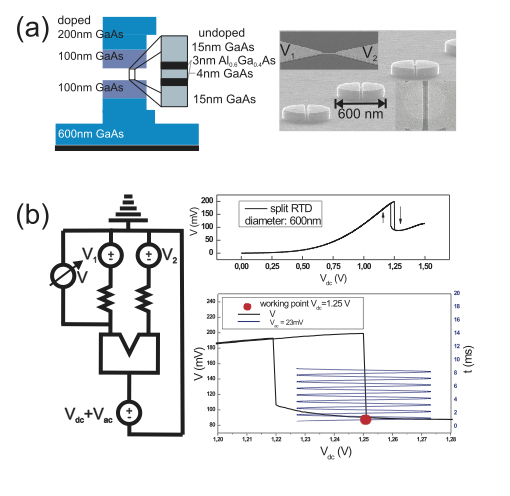
In the upper part of Fig.1 a sketch of the RTD layer sequence is shown. The structure was grown by molecular beam epitaxy. The central part of the RTD is built up by two 3 nm thick AlGaAs barriers embedding a 4 nm thick GaAs layer. Afterward, electron beam lithography and etching were applied for the definition of small mesas with a trench through the upper doped layers. Gold contacts were realized to independently contact the two upper RTD branches further used as input terminals (right part of Fig.1(a)). The measurement circuit diagram is depicted in Fig.1(b). The samples were tested at room temperature in the dark. The RTD shows a resonant peak in the I-V curve at . A hysteresis of was found between the up and down sweep of .
The RTD nanojunctions were tested in the following way (see Fig. 1(b)). At the back contact a working point voltage was applied superimposed by an ac signal with a frequency of . The left and right upper branches were used as inputs with voltages and , respectively. In the right part of Fig.1(b) the working principle is presented. Via the voltage the RTD was driven close to the bistable transition. When the amplitude is ramped up close to a critical threshold voltage, noise-triggered switching can drive the RTD in the upper state. The system is then driven back again to the lower state due to the time-dependent modulation. In the following, it is demonstrated that small voltage changes at the input branches of only a few mV lead to pronounced switching of spike-like signal trains.
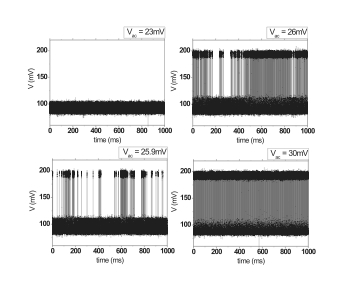
In Fig.2 time traces of the RTD output voltage are shown. The bistable character of the dynamics is apparent. By passing from to the system is changed totally by keeping constant all the other parameters. For the RTD stays in the lower state with . For the RTD is close to the threshold so that noise-induced random jumps from one state to the other appear. By increasing now by only , bursts of spike-like signal trains can be observed. For the upper and the lower state of the RTD are almost equally occupied.
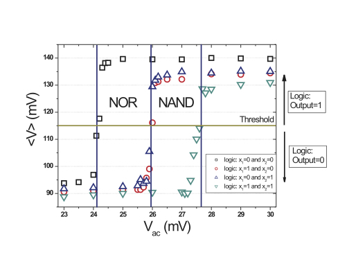
In Fig.3 we show the mean value of as a function of for different input parameter voltages and associated as logic and for and , respectively. A threshold of 115 mV is defined above which the mean is interpreted as a logic output else . We stress the fact that a fairly large output change is produced as a function of a relatively small change in the input. Based on these results we can interpret the functioning of the split RTD in terms of a universal NAND logic gate. Most interestingly the logic functioning of such a gate can be easily changed into that of a logic NOR gate. In fact, as we show in Fig.3 by changing the amplitude of the periodic forcing from mV to the logic behavior changes from NOR to NAND. Such a change happens in a relatively small amplitude range (within ) of the periodic forcing.
In the following we propose a stochastic nonlinear process to model the observed logic function of the split RTD functioning. The model is also capable of predicting a very useful property, i.e. a wide tolerance to the noise affecting the input signals. We start with considering a stochastic dynamic equation, Langevin kind, for the output quantity, that we will call here , subjected to a bistable static potential and a time dependent force .
The time dependent force is composed by three different components:
| (1) |
where is a time periodic signal that, without loss of generality, can be assumed harmonic. is a stochastic force that mimics the presence of noise, that can be assumed exponentially correlated, Gaussian distributed, with zero mean and standard deviation . represents the input signal composed by the composition of the two inputs at the two split RTD branches. represents here the split RTD output whose dynamics can be described as:
| (2) |
To fix our ideas let’s consider the quartic double well potential, but what we are going to say is generically valid for any bistable potential, regardless of the specific analytic form:
| (3) |
where ,, and are suitable constant coefficients.
When the potential is symmetric and in the absence of any external force, i.e. , the system output can assume with equal probability one of the two values corresponding to the two stable minima of the potential . When , the potential is not symmetric anymore and it appears tilted in one direction or the other depending on the sign of . If the potential becomes monostable. When the system output perform a rich dynamics composed mainly by small oscillations around one of the two minima and occasional jumps from one minima to the other, depending on the values of the instant force and of the potential parameters.
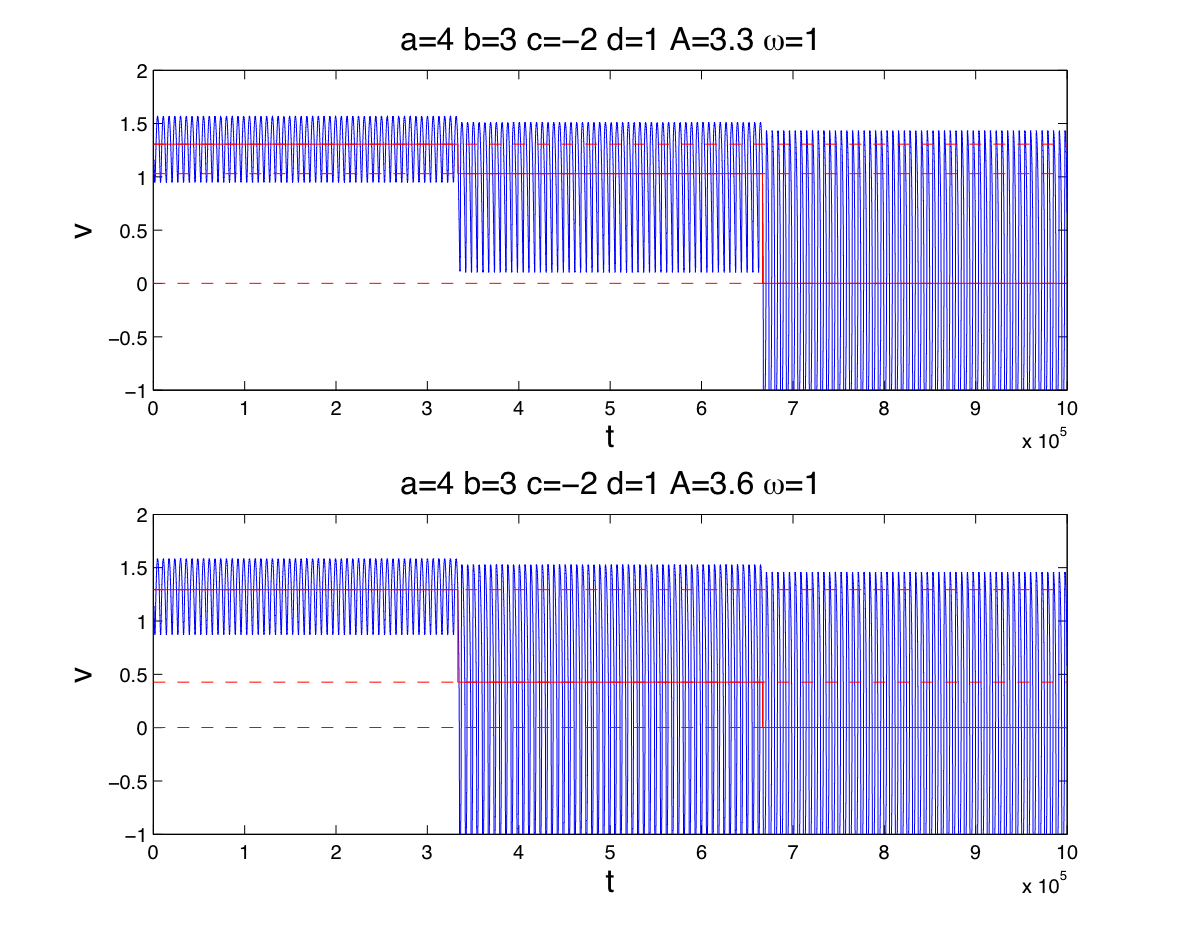
Initially we focus on the behavior illustrated in Fig.2 where the bistable character of the RTD dynamics is exploited in order to perform the NAND/NOR gate functions. In Fig.4 we show the time series for three different combinations of the input values . The output shows an oscillating character, qualitatively similar to in the right parts of Fig.2. Notably, in the upper panel, when the input changes from to to the mean output switches from , to , to . Thus, if we associate the logic state to and the logic state to we have easily reproduced the NAND behavior as shown by the RTD in Fig.3. In the lower panel we show the output for the same conditions of the upper panel but with a value of . In this case the mean output switches from , to , to thus reproducing the NOR behavior. At this point it is easy to compare these results to those in Fig.4 where the change in logic function is obtained for a change of the value of the amplitude of the periodic forcing.
The present strategy aimed at reducing the dissipated power in traditional logic gates based on transistors requires a decrease in the transistors operative voltage thus increasing the vulnerability to the noise. In the following we show that the new scheme just presented for the description of the RTD functioning, shows a significant tolerance to the noise. In Fig.5 we show as a function of the noise standard deviation for the NAND configuration. The continuous line refers to a theoretical prediction that can be easily obtained from:
| (4) |
where
| (5) |
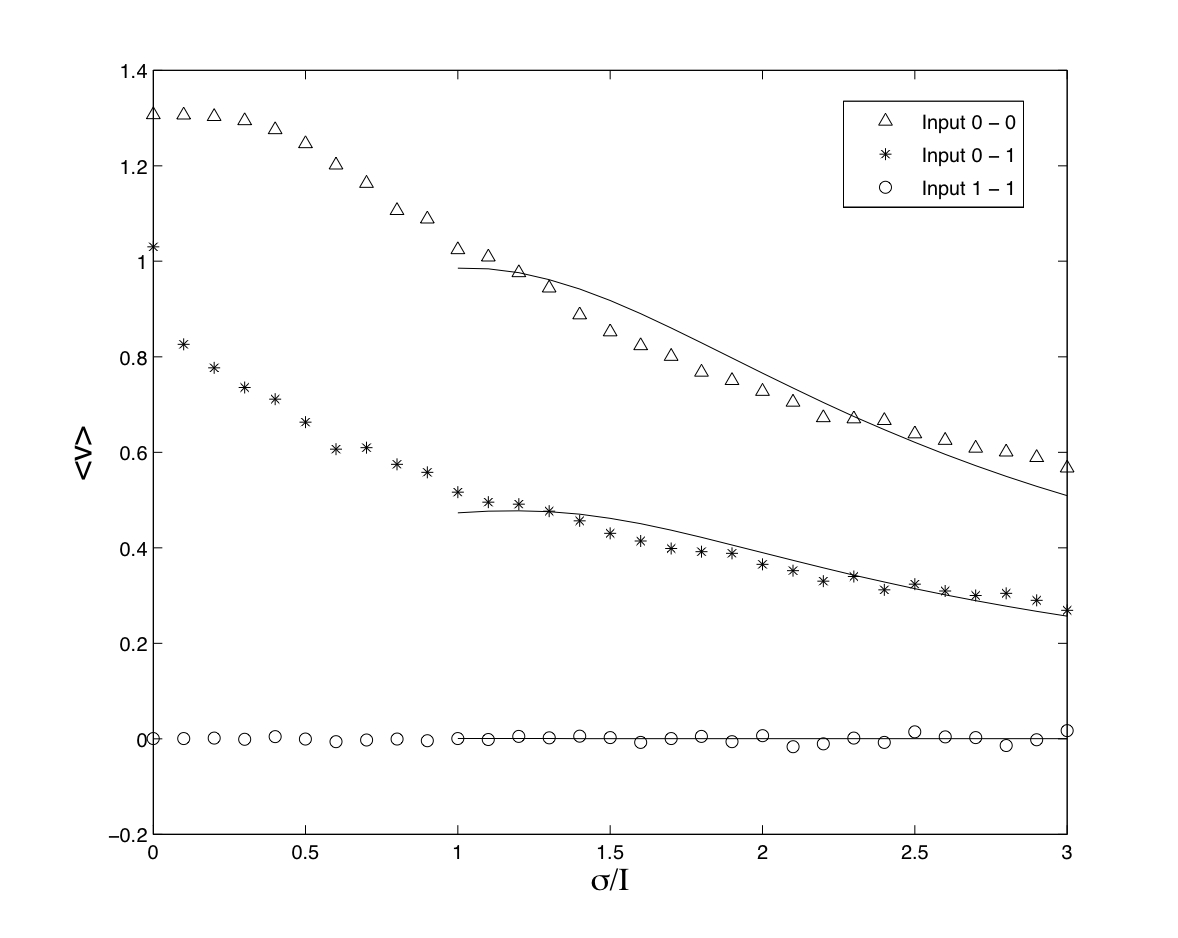
As it can be seen in the figure a logical output coherent with the NAND scheme (logical corresponding to ) is maintained also for noise intensities comparable with the value of the single input. This is quite a remarkable property that could allow the operation of the logic gate in unusually high noise environments. Moreover, with reference to Fig.5 we notice that a lower choice of the threshold value for the logical might allow the operation of the gate also in the presence of a much larger noise. However in this case the re-configurability of the gate from NAND to NOR might be compromised future .
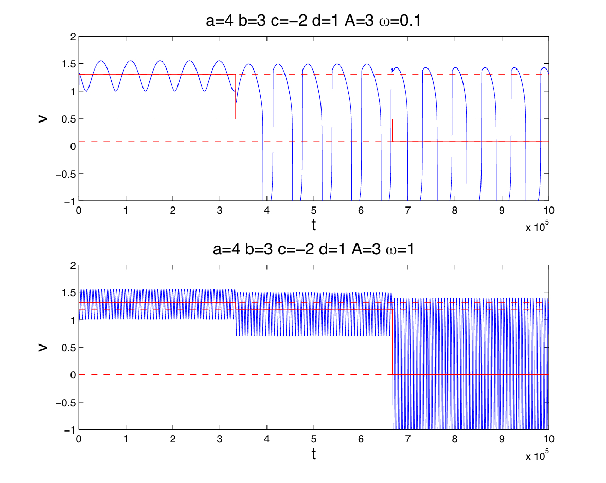
Finally we note that in order to change the configuration from NAND to NOR it is also possible to act on parameters other than . One example is the frequency . In Fig.6 we show the time series for three different combinations of the input values as in Fig.4. Another possibility to reconfigure the gate behavior is to act on the control parameter in eq.(3). Also in this case a small change on this parameter allow a switch between the two logicsfuture .
In conclusion we have presented a novel concept device based on the Resonant Tunneling effect that can be usefully employed as a reconfigurable universal logic gate. The gate can be set to behave as a NAND gate or a NOR gate by simply changing the amplitude of the periodic signal (), its frequency or a DC bias voltage. We have proposed an analytical model based on stochastic nonlinear dynamics that is capable of reproducing all the features experimentally observed on the RTD. Moreover, digital simulations operated on the analytical model indicates that the device functioning is tolerant to noise as large as of the digital input.
The authors gratefully acknowledge financial support from European Commission (FPVI, STREP Contract N. 034236 SUBTLE: Sub KT Low Energy Transistors and Sensors).
References
- (1) L.-M. Duan and R. Raussendorf, Phys. Rev. Lett. 95, 080503 (2005).
- (2) D. Aharonov, A. Kitaev and J. Preskill, Phys. Rev. Lett. 96, 050504 (2006).
- (3) N. Sano, The IEICE Transactions on Electronics, E83-C:1203-1211, Aug. (2000).
- (4) L.B. Kish, Physics Letters A, 305, Issue 3-4, p. 144-149, (2002).
- (5) S. Hanson et al., IBM J. Res. Dev. 50 4/5 (2006).
- (6) K.L. Shepard, V. Narayanan, R. Rose, IEEE Transactions on Computer-Aided Design of Integrated Circuits and Systems, 1132-1150, 18, 8. Aug (1999).
- (7) R.R. Birge, A.F. Lawrence, J.R. Tallent, Nanotechnology 2, p. 73-87, (1991).
- (8) Akram S. Sadek, K. Nikolic, M. Forshaw, Nanotechnology 15, p. 192-210, (2004).
- (9) L. Gammaitoni, Applied Physics Letters, 11/2007, Volume 91, p.3, (2007).
- (10) Krishna V. Palem, IEEE Transactions on Computers, 54(9), pp. 1123-1137, (2005).
- (11) K. Murali, S. Sinha, W. Ditto, A. Bulsara, 2008, submitted
- (12) L. Gammaitoni, P. Hanggi, P. Jung, F. Marchesoni, Rev. Mod. Phys. 70, 1, 223-287 (1998).
- (13) A. R. Bulsara, L. Gammaitoni, Physics Today 49, NO. 3, p. 39, (1996).
- (14) F. Marchesoni, F. Apostolico, L. Gammaitoni, S. Santucci, Phys. Rev. E. 58(6 Part A):7079-7084, (1998).
- (15) H. Risken, The Fokker-Plank Equation, Sprinter, Berlin, (1984).
- (16) F. Hartmann et al. Work in preparation.