Anomalous uniform domain in a twisted nematic cell constructed from micropatterned surfaces
Abstract
We have discovered an optically uniform type of domain that occurs in Twisted Nematic (TN) cells that are constructed from substrates chemically patterned with stripes via microcontact printing of Self-Assembled Monolayers (SAM); such domains do not occur in TN cells constructed from uniform substrates. In such a cell, the azimuthal anchoring at the substrates is due to the elastic anisotropy of the liquid crystal rather than the conventional rubbing mechanism. A model is presented that predicts the relative stability of the twisted and anomalous states as a function of the material and design parameters.
Introduction
One of the most commercially important liquid crystal devices is the twisted nematic (TN) cell (Schadt and Helfrich, 1971), which comprises a nematic liquid crystal film sandwiched between two substrates that have been coated with a rubbed polymer film to promote planar alignment with orthogonal azimuthal easy axes. The local axis of rotational symmetry of the alignment, known as the director, must rotate azimuthally through the depth of the cell in order to satisfy the boundary conditions at both substrates. The total rotation may be either or radians; these two degenerate configurations are referred to arbitrarily as twist and reverse-twist and regions of the cell in each configuration are separated by domain walls as they are topologically distinct. To lift the degeneracy, a polymer that promotes an easy axis at some small angle to the plane of the substrate is used (Fraser, 1978).
Micropatterned surfaces consist of micron-scale regions that promote different easy axes. Away from the distorted surface region, the liquid crystal adopts a bulk orientation that depends on the pattern; by appropriate patterning, it is possible to design a surface to promote an arbitrary effective easy axis. In this spirit, Lee and Clark experimentally showed that a surface micropatterned with alternate planar degenerate and homeotropic stripes will align the liquid crystal azimuthally even though the planar regions are azimuthally degenerate (Lee and Clark, 2001). One of the present authors later showed analytically (Atherton and Sambles, 2006) that in contrast to the usual mechanism, it is the elastic anisotropy that determines the preferred alignment direction so as to minimize the elastic energy. If the twist elastic constant is less than the splay and bend elastic constants, as is the case for most nematic materials, the azimuthal easy axis lies along the length of the stripes. The polar easy axis is determined by the relative width of the planar and homeotropic stripes.
In the present work, we use a striped surface made by microcontact printing of self assembled monolayers (SAMs) of -functionalised alkanethiols (Cheng et al., 2000; Gupta and Abbott, 1997; Bramble et al., 2007) on gold to demonstrate that this elastic-anisotropy mechanism is sufficiently strong to permit the construction of a twisted nematic cell. Since the homeotropic-planar mark-space ratio is 1:1, the cells have a high tilt angle () and exhibit a novel uniform domain forbidden in a conventional TN cell.
Experiment
The micropatterned twisted nematic cell was constructed as follows in cleanroom conditions: Glass microscope slides were used as substrates and were thoroughly cleaned with ultrasonic agitation in detergent (Decon 90), ultra pure water and acetone. The slides were rinsed in water and immersed in pirahna etch (70% sulphuric acid, 30% hydrogen peroxide) for 20 mins. The slides were rinsed and dried in nitrogen before being loaded into a thermal evaporator (Edwards Auto 306). A 3nm layer of Cr was evaporated first, to aid the adhesion of a subsequent 30nm layer of Au. The slides were rotated during evaporation to ensure uniform coverage and to avoid any anisotropy in the roughness of the gold surface which can lead to liquid crystal alignment effects (Gupta and Abbott, 1996).
PDMS (Sylgard 184, Dow Corning) was formed in a ratio of 9 parts elastomer to 1 part curing agent. The mixture was well stirred, degassed under vacuum and poured into a mould containing a Si wafer with 1m etched stripes. Prior to this, the wafer was immersed in a 1 solution of perflurotriethoxysilane (Fluorochem Ltd.) in dichloromethane for 12 hours. This silane monolayer ensures that the cured PDMS can be removed from the etched wafer without breaking (Michel and Bernard, 2001). The PDMS was cured in an oven at 60∘C for 12 hours, carefully cut up into stamps and finally rinsed in ethanol to remove any short chain PDMS material (Kraus et al., 2005).
The PDMS stamps were inked on the printing surface with a 7mM solution in ethanol of perfluorinated alkanethiol (), which is known to promote homeotropic alignment in 6CB(Alkhairalla et al., 1999). The inking solution was allowed to diffuse into the PDMS for approximately 3 mins and then the printed surface was dried with nitrogen. The stamp was then placed on a gold substrate for 3 mins. Good quality printing occurs when the stamp is in conformal contact with the substrate (Bietsch and Michel, 2000), which can be observed during the printing process. The printed surface was then immersed for 12 hours in a 3mM solution in ethanol of mercapto-undecanoic acid (), which is known to promote planar degenerate alignment in 6CB(Alkhairalla et al., 1999). The micropatterned surfaces were then rinsed in clean ethanol and water and then dried.
A cell was constructed from two patterned substrates and 23m PET spacers by first placing the liquid crystal 6CB (Merck) on one surface, heating into the isotropic phase and then placing the second patterned substrate on top with the stripes orthogonal to the first substrate. This procedure was adopted as LC cells which contain perfluorinated alkanethiol SAMs are difficult to fill with liquid crystal by capillary action. The completed cell was then cooled to room temperature.
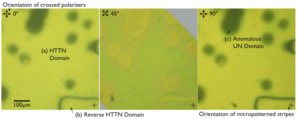
When viewed between crossed polarizers under the microscope, a number of domains become apparent (fig. 1): the majority of the cell [fig. 1(a)] appears bright and remains bright when the cell is rotated azimuthally with the polarisers fixed; other regions [fig. 1(b)] behave in a similar manner, but are separated from the first by dark lines; the final class of regions observed in fig. 1(c) appear dark when the striped surfaces are aligned with the polarizers, but become bright when the cell is rotated with the maximum intensity at . The latter regions are not separated from the former by a distinct line, rather the intensity of transmitted light varies smoothly over a distance of a few microns from that of the surrounding region (which is of the first or second type) to that of the enclosed region (of the third type).
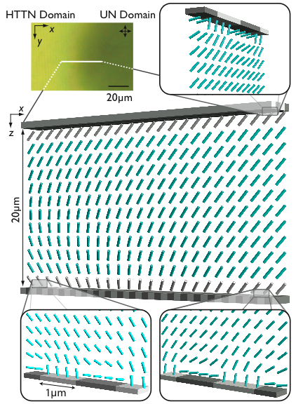
The first and second regions are twist and reverse twist domains typical of a twisted nematic cell and so we shall refer to them as High Tilt Twisted-Nematic (HTTN) states: the director rotates azimuthally by from the bottom substrate to the top substrate. These configurations act as polarisation converters and thus permit transmission independent of azimuthal angle. The optical behaviour of the uniform third region–denoted hereafter the Uniform Nematic (UN) state–is identical to that of a planar cell and so the director in this region must be confined to a plane defined by the surface normal and a vector that points in the direction of one of the sets of stripes. In fig. 2, a possible director profile is shown for the HTTN and UN configurations and an experimentally observed transition region. The UN domains are of particular interest because they are not observed in a conventional twisted nematic cell. No regions are observed that are dark irrespective of orientation with respect to the polarizers (the behaviour of a homeotropic cell).
Model & Discussion
We now construct a model for the observed behaviour by evaluating the energy of the two observed configurations. Let us define a coordinate system local to the surface where the -axis lies along the wavevector of the stripes, the -axis lies along the length of the stripes and the -axis lies perpendicular to the substrate. The director may be parameterized
| (1) |
then the Frank-Oseen elastic energy density
| (2) |
within the approximation has, as was shown in (Atherton and Sambles, 2006), the form
| (3) |
where in which and where the subscripts indicate derivates taken with respect to these coordinates. The Euler-Lagrange equation for the configuration is a scaled version of Laplace’s equation,
| (4) |
with the series solution
| (5) |
where the coefficients , and are determined from the boundary condition. By substituting (5) into (3) and integrating, a general expression for the elastic energy per unit area may be obtained
| (6) |
For a harmonic anchoring potential
| (7) |
where
| (8) |
the natural boundary condition is
| (9) |
where is a characteristic penetration depth of the surface treatment. Since the planar SAMs promote azimuthally degenerate anchoring, there is no azimuthal anchoring term to be considered. Substituting (9) into (5) and exploiting the orthogonality of the and functions, the coefficients
| (10) |
are obtained. The bulk elastic energy per unit area may be evaluated by substituting (10) into (6)
| (11) |
The surface anchoring energy per unit area is obtained by substituting (5) evaluated at and (8) into (7) and integrating
| (12) | |||||
It is now possible to estimate the respective energies of the HTTN state and the UN states using the above expressions. In the UN state the director is oriented at some constant azimuthal angle with respect to the wavevector of the patterning on the lower substrate; there is no bulk elastic deformation and the energy is thus the energy of the distorted surface regions. Since there are two perpendicularly patterned substrates some care must be taken in identifying with , which was defined above with reference to the pattern on one substrate. The total energy of the UN state per unit area, , is
| (13) | |||||
where is associated with the lower substrate and is associated with the upper substrate. This energy has a minimum value when or i.e. when the director is aligned along the length of one or the other of the patterns, which is consistent with the experimentally observed configuration above.
In the HTTN state, the azimuthal orientation is fixed at the surfaces by the elastic anisotropy mechanism such that the component of the director in the plane of the substrate lies along the length of the stripes, and the azimuthal orientation rotates by through the cell thickness. Since the period of the micropatterning the cell thickness, in the middle of the cell the director depends on the -coordinate only. The characteristic penetration length of the distorted surface regions is of order and so the small azimuthal rotation of the director over this length ought to leave the energy due to a distorted surface region unchanged from the situation above where is a constant . The surface contribution to the HTTN state is therefore
| (14) |
It is also necessary to include the contribution from the azimuthal rotation of the director in the bulk. In contrast to the conventional TN cell, the polar angle is not constant throughout the cell; the director can reduce the magnitude of the twist deformation by tilting towards homeotropic in the centre of the cell at the expense of a slight splay or bend deformation. From recent simulation of the HTTN state (Atherton and Sambles, 2007), a suitable ansatz for the bulk director configuration is
| (15) |
where the amplitude of the perturbation , the magnitude of the tilt perturbation, is a free parameter that must be varied so as to minimize the total free energy. Routine substitution of (15) into the Frank energy (2) yields after integration an energy per unit area
| (16) |
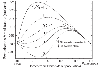
where is a Bessel function of the first kind and is the Struve function. The energy must be minimized numerically with respect to . Typical perturbation amplitudes are plotted in fig. 3 as a function of the homeotropic-planar pattern mark-space ratio which is assumed to be the same on both substrates; above a certain threshhold value of , the tilt perturbation is always toward the homeotropic orientation, i.e. is always positive; below this value the tilt perturbation is towards planar for low and towards homeotropic for high . The energy of the HTTN state is then
| (17) |
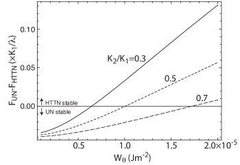
From the expressions for and , the difference between the energies of the two states was calculated for a variety of polar anchoring strengths and elastic constant ratios (fig. 4), using the design parameters for the experimental pattern, i.e. and and the absolute magnitude of which is comparable with experimental measurements for 6CB (Karat and Madhusudhana, 1977; Madhusudhana and Pratibha, 1982); the critical anchoring energy below which the UN state has lower energy than the HTTN state is about .
Conclusion
A twisted nematic cell has been constructed using substrates micropatterned with SAMs by microcontact printing. Characteristic twisted and reverse twisted states have been observed in the cell, however these are stabilized not by azimuthal anchoring as in a conventional TN device, but by a recently elucidated elastic anisosotropy mechanism due to rapid variation of the polar easy axis. This mechanism promotes rather weak azimuthal anchoring which, if the polar anchoring energy is sufficiently weak, may be of comparable energy to the bulk twist; facilitating a transition from the twist or reverse-twist states to a uniform state that is not facile in conventional TN cells due to the much higher azimuthal anchoring energy. We found the critical polar anchoring energy for such a transition to be .
A further feature of the micropatterned TN cell is that the pretilt angle is much larger () than in a conventional TN display and readily controllable by adjusting the design parameters of the patterning. An interesting phenomenon has been elucidated that should be exhibited by any high pretilt TN device regardless of the anchoring mechanism: there is a spontaneous tendency for the director to tilt towards the planar or homeotropic orientations depending on the relative magnitude of and .
The SAMs technique has for the first time been demonstrated to permit the fabrication of device-scale patterns, and the rich phase diagrams that arise in cells constructed from micropatterned surfaces suggest the possibility of interesting additional phenomena such as bistability.
Acknowledgements.
The authors would like to thank Sharp Laboratories of Europe for financial support and N. J. Smith, S. A. Jewell and C. Rosenblatt for helpful discussions. This work was supported by the Engineering and Physical Research Council, Grant No. GR/S59826/01.References
- Schadt and Helfrich (1971) M. Schadt and W. Helfrich, Appl. Phys. Lett. 18, 127 (1971).
- Fraser (1978) C. Fraser, J. Phys. A 11, 1439 (1978).
- Lee and Clark (2001) B. Lee and N. A. Clark, Science 291, 2576 (2001).
- Atherton and Sambles (2006) T. J. Atherton and J. R. Sambles, Phys. Rev. E 74, 022701 (2006).
- Cheng et al. (2000) Y. L. Cheng, D. N. Batchelder, S. D. Evans, J. R. Henderson, J. E. Lydon, and S. D. Ogier, Liq. Cryst. 27, 1267 (2000).
- Gupta and Abbott (1997) V. Gupta and N. Abbott, Science 276, 1533 (1997).
- Bramble et al. (2007) J. P. Bramble, S. D. Evans, J. R. Henderson, C. Anquetil, D. J. Cleaver, and N. J. Smith, Liq. Cryst. 34, 1059 (2007).
- Gupta and Abbott (1996) V. K. Gupta and N. L. Abbott, Langmuir 12, 2587 (1996).
- Michel and Bernard (2001) B. Michel and A. Bernard, IBM J. Res. & Dev. 45, 697 (2001).
- Kraus et al. (2005) T. Kraus, R. Stutz, T. E. Balmer, H. Schmid, L. Malaquin, N. D. Spencer, and H. Wolf, Langmuir 21, 7796 (2005).
- Alkhairalla et al. (1999) B. Alkhairalla, H. Allinson, N. Boden, S. D. Evans, and J. R. Henderson, Phys. Rev. E 59, 3033 (1999).
- Bietsch and Michel (2000) A. Bietsch and B. Michel, J. Appl. Phys. 88, 4310 (2000).
- Atherton and Sambles (2007) T. J. Atherton and J. R. Sambles, Mol. Cryst. Liq. Cryst. 475, 3 (2007).
- Karat and Madhusudhana (1977) P. P. Karat and N. V. Madhusudhana, Mol. Cryst. Liq. Cryst. 40, 239 (1977).
- Madhusudhana and Pratibha (1982) N. V. Madhusudhana and R. Pratibha, Mol. Cryst. Liq. Cryst. 89, 249 (1982).