Experimental Determination of
the Gain Distribution of
an Avalanche Photodiode at Low Gains
Abstract
A measurement system for determining the gain distributions of avalanche photodiodes (APDs) in a low gain range is presented. The system is based on an ultralow-noise charge–sensitive amplifier and detects the output carriers from an APD. The noise of the charge–sensitive amplifier is as low as 4.2 electrons at a sampling rate of 200 Hz. The gain distribution of a commercial Si APD with low average gains are presented, demonstrating the McIntyre theory in the low gain range.
Index Terms:
Avalanche photodiode, gain distribution, charge-sensitive amplifier.I INTRODUCTION
Gain distribution is an important characteristic of avalanche photodiodes (APDs). The most widely used theory for understanding the gain distribution of APDs is that of McIntyre[1]. In the McIntyre theory, the electron and hole ionization coefficients and are considered to depend only on the local electric field. From this assumption, it is found that the gain distribution in the McIntyre theory is considerably different from the Gaussian distribution. The gain distribution for a single-carrier injection, for example, has a peak at a gain of one for any value of the average gain.
By using the Monte Carlo simulation to investigate the improvement in the avalanche noise performance of APDs, Ong et al. found that for a single-carrier injection, the peak in the gain distribution of thin p+–i–n+ GaAs APDs was shifted closer to the average gain[2]. They showed that at an average gain of 5.1, the APD had a peak at a gain of two, whereas conventional APDs have a peak at a gain of one. These results provide hope for the improvement of the photon detection efficiency in the detection of single photons when the APDs are operated in the linear and sub-Geiger modes[3]. If the peak shifts considerably closer to the average gain, the APD may have the ability to resolve the photon number[4, 5]. This behavior is caused by the dead space effect. The dead space is the space where impact ionization cannot occur and increases with decreasing length of the multiplication region. And because of the dead space effect, the randomness of impact ionization process decreases. Then, the gain distributions have a peak around the average gain for shorter devices. On the other hand, the dead space reduces with excessive electron field intensity because the carriers quickly gain sufficient energy to initiate an ionization event. That is, this behavior has been found in APDs with thin multiplication region ( 1 m) and low average gains currently.
Unfortunately, the gain distribution that are expected to exhibit low excess noise in contradiction to the McIntyre theory has not been experimentally determined so far. Conventional charge-sensitive amplifiers that have been widely used to determine gain distributions [6, 7, 8] produce noise greater than several hundred electrons, and hence, they fail in characterizing the gain distributions of low-noise APDs at low average gains. We have also developed an ultralow-noise charge-sensitive amplifier based on a capacitive transimpedance amplifier (CTIA)[4, 5]; however, we have never succeeded in determining the gain distribution for single-carrier injection because of the large noise and drift of the amplifier[9, 10]. In this letter, we demonstrate the determination of the gain distribution for a single-carrier injection in low gain ranges by improving the noise characteristics of the charge-sensitive amplifier.
II EXPERIMENTAL SETUP
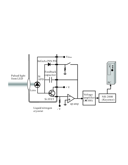
Fig. 1 shows the experimental setup. We used a APD (S8890-02, Hamamatsu Photonics) with thick multiplication region ( 1 m). The gain distribution of this type of APD can usually be explained by McIntyre noise theory. Then, it would be possible to compare the gain distribution measured by our system with the predictions of McIntyre noise theory, and hence to test our measurement system.
The CTIA [4, 5] comprised a silicon JFET (Si JFET), a feedback capacitor, an InGaAs PIN PD for discharging the capacitor and an operational amplifier (op amp). The Si APD sample was mounted on a SiO2 glass platform containing three of the circuit elements of the CTIA (the Si JFET, feedback capacitor and InGaAs PIN PD). The glass platform was set on the work surface of a cryostat and was cooled to 77 K with the aid of liquid nitrogen to suppress leak current of semiconductor devices and thermal noise. The CTIA circuit noise was as low as 4.2 electrons at a sampling rate of 200 Hz.
The light signal was produced by a 450-nm LED, and was focused on the Si APD. The wavelength of the LED was chosen to be such that a pure hole injection was caused. We tried to measure the gain distributions under the pure electron and pure hole injection conditions and compared them with the predictions of McIntyre noise theory. We found that it is actually the case of hole injection at 77 K. The signal was modulated to yield pulses with a width of 0.5 ms at a repetition rate of 200 Hz. To satisfy the conditions for a single-carrier injection, the light signal intensity was heavily attenuated using neutral density filters so that the average number of initial holes was 0.1 per pulse and the probability of generation of more than two holes was negligible.
The output voltage corresponding to carriers generated from the APD is given by
| (1) |
where is the elementary charge and is the capacitance of the feedback capacitor. In our present system, 0.07 pF so that a single output carrier () induces an output voltage of 2.3 V. This output voltage is further amplified by a manually fabricated voltage amplifier with a gain of 100 and a noise level of 0.4 electrons (r.m.s.). We digitize the amplified output signals using a data acquisition system (NR-2000, Keyence), and then store the digitized data in a computer. From the stored data, we obtained the gain distribution of the APD.
The mean dark current of the APD was 0.04 electrons/pulse. This value was sufficiently less than the average number of initial holes. We measured the dark current after the warm-up drift was stabilized, which took several hours.
III EXPERIMENTAL RESULTS
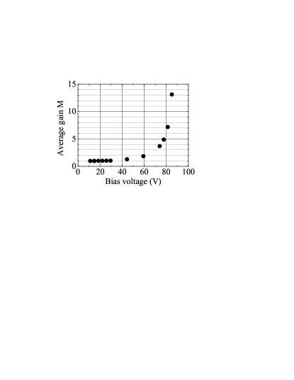
Before presenting the gain distribution for a single-carrier injection in the low gain range, we discuss the basic characteristics of the Si APD sample. Fig. 2 shows the average gain curve as a function of the bias voltage at 77 K. We measured the gain characteristic by using the setup of Fig. 1 except the average number of initial holes was 48 per pulse. The average gain of the APD is defined to be unity for a bias voltage of 18.5 V since the average number of output carriers remains constant around this voltage.
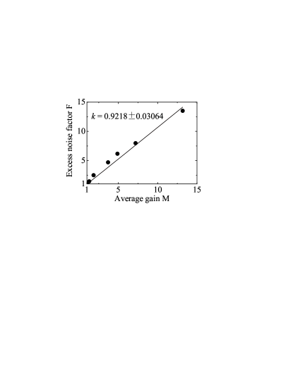
The excess noise factor is given by
| (2) |
where, is a statistical variable that describes the multiplication gain, and denote statistical (ensemble) averaging, i.g. . We computed the from analysis of the gain distributions obtained by the previous experiment. Fig. 3 shows the excess noise factor as a function of the average gain. The obtained data are shown by dots, whereas the theoretical fit is shown by the solid curve, which is obtained from the theory of McIntyre for the hole injection alone [11]
| (3) |
We also estimated the ratio of the hole to electron ionization coefficients ( and , respectively) as 0.9218 0.03064.
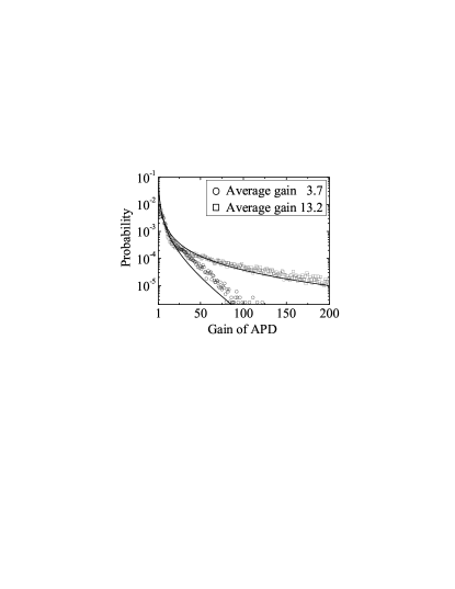
Fig. 4 shows the obtained gain distribution at an average gain () of 3.7 and 13.2. The average number of initial holes was 0.1 per pulse so that the almost avalanche multiplication was caused by single-carrier (here hole) injection. The solid curve is the theoretical curve given by
| (4) |
where is the probability of obtaining a single hole in a pulse, i.e., . is the probability
| (5) | |||||
that an initial single hole will result in a total of holes. We can observe fairly good agreement between the measurements and the theoretical curve. This demonstrates that the APDs considered in this study can be described well by the McIntyre theory; to the best of our knowledge, this demonstration is the first in a low gain range.
IV CONCLUSION
We have described the measurement system for obtaining the gain distributions of APDs in a range of low average gains. The key technology is an ultralow–noise CTIA and detects the carriers generated in an APD. We have presented the obtained gain distribution of an Si APD for an average gain () of 3.7 and 13.2 for a single-hole injection.
The next important step is to employ our system for the investigation of the gain distributions of various types of APDs that are expected to exhibit low excess noise in contradiction to the McIntyre theory[12, 13, 14, 15, 16, 17]. These low-noise APDs are promising devices for use as single-photon APDs with high photon detection efficiency since the efficiency increases with a decrease in the avalanche multiplication noise. Our measurement setup can be a powerful tool for predicting the performance of single-photon APDs.
Acknowledgment
The authors thank Etsuro Sasaki for technical support.
References
- [1] R. J. McIntyre, ”The distribution of gains in uniformly multiplying avalanche photodiodes: Theory,” IEEE Trans. Electron Devices, vol. ED-19, pp. 703–713, Jun. 1972.
- [2] D. S. Ong, K. F. Li, G. J. Rees, J. P. R. David, P. N. Robson, and G. M. Dunn, ”Monte Carlo estimation of avalanche noise in thin p+–i–n+ GaAs diodes,” Appl. Phys. Lett., vol. 72, pp. 232–234, Jan. 1998.
- [3] H. Dautet, P. Deschamps, B. Dion, A. MacGregor, D. MacSween, R. McIntyre, C. Trottier, and P. Webb, ”Photon counting techniques with silicon avalanche photodiodes,” Appl. Opt., vol. 32, pp. 3894–3900, Jul. 1993.
- [4] K. Tsujino, M. Akiba, and M. Sasaki, ”Ultralow-noise readout circuit with an avalanche photodiode: Toward a photon-number-resolving detector,” Appl. Opt., vol. 46, pp. 1009–1014, Mar. 2007.
- [5] K. Tsujino, M. Akiba, and M. Sasaki, ”A charge-integration readout circuit with a linear-mode silicon avalanche photodiode for a photon-number resolving detector,” Optics and Spectroscopy, vol. 103, pp. 86–89, Jul. 2007.
- [6] J. Conradi, ”The distribution of gains in uniformly multiplying avalanche photodiodes: Experimental,” IEEE Trans. Electron Devices, vol. ED-19, pp. 713–718, Jun. 1972.
- [7] Nathan G. Woodard, Eric G. Hufstedler, and Gregory P. Lafyatis, ”Photon counting using a large area avalanche photodiode cooled to 100 K,” Appl. Phys. Lett., vol. 64, pp. 1177–1179, Mar. 1994.
- [8] A. Dorokhov, A. Glauser, Y. Musienko, C. Regenfus, S. Reucroft, J. Swain, ”Study of the Hamamatsu avalanche photodiode at liquid nitrogen temperatures,” Nucl. Instr. and Meth. A, vol. 504, pp. 58–61, May. 2003.
- [9] M. Akiba, M. Fujiwara, and M. Sasaki, ”Ultrahigh-sensitivity high-linearity photodetection system using a low-gain avalanche photodiode with an ultralow-noise readout circuit,” Opt. Lett., vol. 30, pp. 123–125, Jan. 2005.
- [10] K. Tsujino, M. Akiba, and M. Sasaki, ”Measurement system for acquiring gain distributions of avalanche photodiodes at low gains,” Proceedings of SPIE, vol. 6771, pp. 0Z-1–0Z-8, Sep. 2007.
- [11] R. J. McIntyre, ”Multiplication noise in uniform avalanche diodes,” IEEE Trans. Electron Devices, vol. ED-13, pp. 164–158, Jan. 1966.
- [12] C. Hu, K. A. Anselm, B. G. Streetman, and J. C. Campbell, ”Noise characteristics of thin multiplication region GaAs avalanche photodiodes,” Appl. Phys. Lett., vol. 69, pp. 3734–3736, Dec. 1996.
- [13] K. F. Li, D. S. Ong, John P. R. David, G. J. Rees, Richard C. Tozer, Peter N. Robson, and R. Grey, ”Avalanche multiplication noise characteristics in thin GaAs p+–i–n+ diodes,” IEEE Trans. Electron Devices, vol. 45, pp. 2102–2107, Oct. 1998.
- [14] K. Sawada, M. Akiyama, and M. Ishida, ”Excess noise characteristics of amorphous silicon staircase photodiode films,” Appl. Phys. Lett., vol. 75, pp. 1470–1472, Sep. 1999.
- [15] M. Moszyński, M. Kapusta, M. Balcerzyk, M. Szawlowski, D. Wolski, I. Wȩgrzecka, and M. Wȩgrzecki, ”Comparative study of avalanche photodiodes with different structures in scintillation detection,” IEEE Trans. Nucl. Sci., vol. 45, pp. 1205–1210, Aug. 2001.
- [16] V. N. Solovov, F. Neves, V. Chepel, M. I. Lopes, R. F. Marques and A. J. P. L. Policarpo, ”Low-temperature performance of a large area avalanche photodiode,” Nucl. Instr. and Meth. A, vol. 504, pp. 53–57, May. 2003.
- [17] T. Ikagawa, J. Kataokaa, Y. Yatsua, N. Kawaia, K. Morib, T. Kamaec, H. Tajimac, T. Mizunoc, Y. Fukazawad, Y. Ishikawae, N. Kawabatae and T. Inutsuka, ”Performance of large-area avalanche photodiode for low-energy X-rays and -rays scintillation detection,” Nucl. Instr. and Meth. A, vol. 515, pp. 671–679, Dec. 2003.