Grounded Uniaxial Material Slabs as Magnetic Conductors
Abstract
The objective of this paper is all-angle artificial magnetic conductor, i.e. artificial magnetic conductor that has stable magnetic-wall effect with respect to the incidence angle. Furthermore, we seek for a design that would be easy for manufacturing. In order to achieve this we use grounded uniaxial material slabs and we do not constrict ourselves to naturally available materials. Instead, we assume that the desired parameters can be synthesized using the emerging artificial electromagnetic materials. It is found that it is possible to have an all-angle magnetic-wall effect for both TE and TM polarization. Especially for the TM fields the structure would be easily manufacturable. The proposed structure has similar appearance as more well-known artificial impedance surfaces, but the design parameters and the physical properties behind the magnetic wall effect are novel. The performance of the proposed artificial magnetic conductor is verified with numerical simulations. This paper introduces a new approach how to obtain a magnetic-wall effect. It is possible to use this this approach also together with other ways of obtaining the magnetic-wall effect for dual-band operation.
Vol. x, y–z, 2004
O. Luukkonen: olli.luukkonen@tkk.fi
1 Introduction
Artificial magnetic conductors (AMC) have been studied widely in the literature after the seminal paper of D. Sievenpiper et al. published in 1999 [1]. Especially, the use of these surfaces for lowering the height of horizontal wire antennas has attracted much attention. In [1, 2, 3, 4, 5, 6, 7, 8, 9] artificial magnetic conductors have been realized as a certain resonant structure, not involving resonant magnetically or electrically polarizable particles. In the vicinity of the structure resonance the surface impedance becomes very high in the absolute value, making the use of these surfaces as magnetic conductors possible. In corrugated surfaces the quarter-wavelength resonances can be utilized in a similar way (see e.g. [10]). In addition to resonant structures, also more conventional materials (in the sense of magnetic or electric polarizations excited by magnetic or electric stimuli) have been studied [11, 12, 13, 14]. In these cases the materials have been considered without paying attention to the possible anisotropy. In [13] it was shown that the radiation properties of a horizontal dipole can be improved by a substrate implemented as a grounded slab with nearly zero permittivity. Such a substrate operates as a magnetic conductor for all angles of incidence of TM-polarized electromagnetic waves.
The uniaxial symmetry of the structure is the most general allowed symmetry, if the magnetic-wall effect should be isotropic in the surface plane. Thus, we will study the most general approach to the realization of the all-angle magnetic walls using material layers. The fully isotropic layers are a special case covered by this theory, but we expect that allowing uniaxial anisotropy will make the actual realization much simpler. Indeed, to engineer, for example, passive materials one needs inclusions which are inherently anisotropic. Naturally, it is possible to manufacture isotropic materials from anisotropic inclusions by grouping and orienting the particles in such a way that an electric or a magnetic stimuli along all of the orthogonal direction will create the same response. This is, however, a troublesome and most likely impractical way, if electrically thin realizations are needed. The possibility to avoid the requirement of full 3D isotropy would greatly simplify the structure and its manufacturing.
In this paper we systematically study what uniaxial material property can allow us to realize all-angle magnetic conductors. We will not restrict ourselves to the naturally available materials but assume that the desired parameters can be synthesized using emerging metamaterials (e.g., [15]). In a uniaxial material, the relative permittivity or permeability have different values along the transversal and normal axes (defined with respect to the surface of the material slab). Uniaxial materials provide hence an extra degree of freedom compared to the conventional materials. As we will see, the use of artificial materials with extreme parameters offers a possibility for design of structures with superior performance, not achievable with conventional materials.
In the following section II we derive the needed analytical models for the analysis of the grounded uniaxial material slabs. In sections III and IV we use these models to study what kind of material parameter values are needed for all-angle magnetic conductors for the TM and TE fields, respectively. The study reveals that for the TM fields it is sufficient to have just the normal component of the permittivity to be close to zero. This can be done by using wire medium at its plasma frequency and suppressing its spatial dispersion. In section V we will discuss the issue of suppression of the spatial dispersion in the wire medium. An example of the structure is given in section VI in which we also verify our result by simulations.
2 Surface impedance of a grounded uniaxial material slab
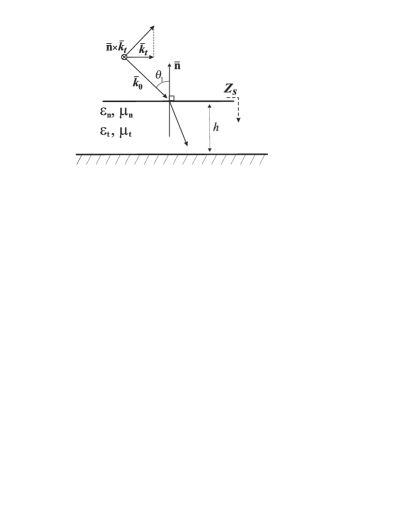
In Fig. 1 a schematic picture of a grounded uniaxial material slab is shown. The properties of the material slab are described by the effective transverse and normal permittivities ( and ) and permeabilities ( and ), respectively. It is convenient to model the structure shown in Fig. 1 with a surface impedance at the top interface of the structure. This surface impedance can be calculated through the transmission-line model illustrated by Fig. 2 [9]. For this we need both the wave impedance and the normal component of the wave number in the uniaxial material of the substrate.
The wave impedances in the uniaxial material read for TE- and TM-polarized incident plane waves, respectively, as [16]:
| (1) |
| (2) |
Here, the normal components of the wave vectors in the uniaxial slab read [16]:
| (3) |
| (4) |
where is the transverse wave number. Using the transmission-line model in Fig. 2 and 1–4, we can write the surface impedances for both polarizations as (see also [17]):
| (5) |
| (6) |
In order to realize a magnetic conductor, the absolute values of these expressions need to be maximized.
Let us next look more closely into the cases of TM and TE polarizations separately. Our goal for both polarizations is to realize a magnetic conductor whose performance would not be affected by the incident angle nor by the finite electrical thickness of the slab.
3 Magnetic conductors for TM polarization
The main problems for artificial magnetic conductors are the frequency and angular dependencies of the magnetic wall effect. A grounded dielectric slab with the quarter-wavelength electrical thickness serves as a good example here. The magnetic wall effect due to the -thickness of the slab is clearly highly dependent on the frequency. In the case of low relative permittivity of the substrate the effect is also highly dependent on the incidence angle. The magnetic wall effect moves to higher frequencies as the incidence angle grows. It is desirable to decrease both frequency and angular dependencies of the magnetic wall effect.
We first study the properties of uniaxial material slabs for which the transverse and normal components of the relative permeability are both positive and the components of the permittivity are arbitrary chosen. We will then study the inverse case when the transverse component of the permeability is arbitrary chosen. For simplicity of the analysis we neglect the losses in the structure.

Let us first consider reducing the periodical dependency of the surface impedance on the frequency by designing an imaginary . This would mean that the waves propagating along the normal to the surface in the uniaxial material slab would be evanescent. In the case when we approach the singularity of 4 and we can approximately write the normal component of the wave vector in the uniaxial material slab for obliquely incident plane waves as
| (7) |
For the normal incidence () the incident plane wave has no electric field component along the normal and therefore the normal component of the permittivity has no effect. We can now write the surface impedance of the grounded uniaxial slab for oblique incidence using 6 and 7 as:
| (8) |
For TM polarization inductive surfaces support surface waves, because the surface impedance for the evanescent TM-polarized plane wave in free space is , where and is the free-space wave impedance. We see from 8 that in this case the surface does not support TM-polarized surface waves, and its surface impedance is not a periodic function of the frequency. More importantly, we see that as approaches zero, the surface impedance for the TM polarization tends to .
For the case when we can write the surface impedance 6 as:
| (9) |
We see that when the waves do not become evanescent in the uniaxial material slab and the surface impedance 9 becomes a quickly oscillating function of . The surface operates as a magnetic conductor either for a narrow frequency band or for a limited range of incidence angles. However, we can overcome this drawback by choosing the tangential component of the permittivity to be negative instead of and make the fields propagating along the normal of the surface evanescent in the material slab. For negative values of the permittivity and in cases when , we can replace the tangent with the hyperbolic tangent and with its absolute value in 9.
Let us next look at the case of electrically thin material slabs. In this case we can replace the tangent function by its argument. Choosing and we make the uniaxial material slab electrically thin. In this case a near-zero value of the transversal permittivity is not needed for realization of a high surface impedance:
| (10) |
Instead a high- or a low- material is needed. In terms of surface wave suppression, the latter choice outperforms the former. Unfortunately, the latter choice will lead to a situation where the performance of the magnetic conductor deteriorates in the vicinity of the incidence angle defined by
| (11) |
where is the angle of incidence and is the speed of light in free space. In the case the approximation of the electrically thin substrate results in the following conditions for the transverse components of the permittivity:
| (12) |
These conditions are difficult to satisfy because of the complexity of the needed uniaxial grounded material slab structure. First, we would need to have metallic wires (for near-zero values of the relative permittivity) in all three directions. Secondly, we would need to add split-ring resonators or similar inclusions (for high values of relative permeability). We can conclude that the regime of electrically thin substrate leads to the situation where either the performance of the magnetic conductor deteriorates at a certain incidence angle or the realization of the magnetic conductor is difficult.
In the case of a very high (the normal component of has no effect on the incident wave in the TM case), most of the incident wave power is refracted along the normal. Then the response of the slab becomes weakly dependent on the incidence angle, since
| (13) |
In addition to this, the slab becomes electrically thick which results in quickly oscillating (with respect to the frequency) surface impedance.
From the discussion above we see that it is possible to realize artificial magnetic conductors for TM polarization by having one of the components of close to zero. is a suitable choice if we tolerate the loss of the magnetic wall effect at the angle . Realization of the high surface impedance over a wide frequency band or over a wide range of incidence angles otherwise is not possible without specially adjusting the value of one of the three remaining material parameters.
4 Magnetic conductors for TE polarization
For the TE polarization the case of the grounded uniaxial material slab becomes different than for its counterpart TM polarization discussed in the previous section. The surface impedance in 5 is more dependent on the permeability rather than permittivity. In order to realize a magnetic conductor from an isotropic material, the value of the permittivity needs to be minimized and the value of the permeability maximized (see also 5 and 6). For this reason the singularity of 3 does not play so significant role as it does for the TM polarization. Instead, we concentrate on the regime .
In order to minimize the angular dependency of the magnetic conductors, we should have . Then we have from 3 and 1:
| (14) |
For a high surface impedance we still need to maximize , which unfortunately leads to quick oscillations of along the frequency axis. We can overcome this drawback by decreasing the transverse permittivity and thus complicating the layer structure.
We can also decrease the angular dependency of the surface impedance by having the transverse permittivity approach zero: . In this case the surface impedance of TE polarized incident waves reads
| (15) |
Obviously we still need to maximize the transverse permeability in order to realize a magnetic conductor.
The magnetic wall effect realized by using grounded uniaxial material slabs for the TE polarization does not seem to offer such advantages as for the TM polarization. For the TM polarization it is sufficient to engineer only the normal component of the effective permittivity correctly in order to realize a magnetic conductor. The case of the TE polarization is not so simple; for the TE polarization at least two effective material parameters need to be engineered in the transverse direction. Practically this means orienting two different type of particles (magnetic and electric) in two orthogonal directions.
5 Practically realizable uniaxial magnetic conductors

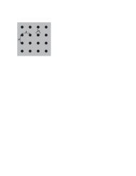
The wire medium serves as a good example of a uniaxial electromagnetic crystal that can possess near zero values of the effective permittivity. Based on the discussion in the previous sections the most promising case is to use this feature for realizing magnetic conductors for TM polarization. In this case the wires should be oriented normally to the surface. For TE-polarized incident fields these wires have no effect. This type of grounded wire medium slab structures, or ”Fakir’s bed of nails”, have been studied earlier in [18, 19] (see Fig. 3). In [18] the wire medium slab comprised densely packed wires, and the height of the slab was large compared to the period of the wire medium. The surface impedance for such a structure reads:
| (16) |
as was shown also in [19]. For this type of structures we see that the near-zero value of the normal component of the permittivity tensor has no effect on the surface impedance, but the TEM modes of the wire medium become dominant (see, e.g. [16], p. 231). Furthermore, structures with densely packed metallic vias are expensive to manufacture. Instead, thin slabs with rather sparse wires are preferred in practical applications. In this case also the TM modes excited in the wire medium slab become significant. In the following, we will discuss the structure needed for realizing the wide-angle and wide-band magnetic conductors for the TM polarization. However, in practical applications the bandwidth of the magnetic conductor is reduced by the limited frequency band for which the wire medium posses near-zero values for the effective permittivity.
The wire medium is known to be strongly spatially dispersive material whose effective permittivity can be described for our case as [20, 21, 22]:
| (17) |
where is the relative permittivity of the host medium, is the plasma wave number, is the wave number in the host medium, and is the -component of the wave vector. This non-local homogenization model predicts that in the case of TM-polarized incident waves two modes can be excited in the wire medium with different values for . In this case the definition of the for the wire medium slab becomes non-explicit and the reflection properties of such slabs need to be solved by calculating the fields of both modes in the slab [19]. In addition to this, the study in the previous sections becomes not applicable in the spatially dispersive case. For these reasons we need to suppress the spatial dispersion in the wire medium slab.

Suppression of the spatial dispersion in wire medium has been studied recently in [23, 25, 24, 26]. In [23] the spatial dispersion was suppressed by connecting the parallel wires capacitively to each other. This is similar to the situation in [25, 24, 26] where it was first noticed that the spatial dispersion in the wire medium slab covered with metallic patches is suppressed when choosing the height and the lattice constant of the wire medium slab properly. In these cases the local (non-spatially dispersive) model is valid for the effective value of the normal component of the permittivity, and it reads:
| (18) |
The plasma wave number can be estimated as [21]:
| (19) |
where is the lattice constant of the wire medium and is the radius of the vias (see Fig. 4).
The explanation of the suppression of spatial dispersion in the wire medium is simple. The presence of patches makes the currents induced in the wires by the incident TM-polarized waves practically uniform over the height . It is so if , since in this case the induced charges are practically concentrated at the patches’ edges. The absence of charge accumulation on the wires ensures the practical uniformity of currents. Though mathematically the currents along the wires can still be presented as a sum of the TEM and TM modes, the smallness of the current variation across the wire medium slab means that the propagation effect of these modes over the height is negligible. Since the waves in the wire medium slab can propagate only in the horizontal plane, one can consider the wire medium slab as a uniaxial dielectric with negative below the plasma frequency.
6 An example and numerical validation
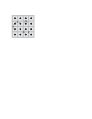
Here we concentrate on validating our results for the TM polarization using an example that follows the design of [25, 24, 26]. In our example shown in Fig. 4 we have included metallic patches on top of the wire medium slab so that each patch is galvanically connected to just one via. The structure has similar appearance to the mushroom structure. However, here we do not utilize the structure resonance. Instead, we utilize the near-zero value of the normal component of the permittivity of the wire medium slab in order to create a magnetic conductor. To demonstrate that the magnetic conductor effect of the surface relates to the near-zero value of the normal component of the permittivity we have used qualitatively the design equations of [8]. These equations allow us to design the resonance frequency of the structure (the mushroom type of high-impedance surfaces) far away from the frequency region where we would have .
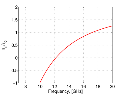
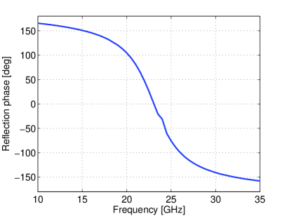
We have chosen the parameters of the non-spatially dispersive wire medium slab to be the following: mm, mm, mm, , and mm. For these parameters the normal component of the effective permittivity tends to zero approximately at GHz and the mushroom structure resonance is approximately at GHz as shown in Figs. 5 and 6(a), respectively. For the normal incidence the vias do not have any effect on the plane-wave response of the structure, and the resonance shown in Fig. 6(a) is solely due to the other structural properties of the wire medium slab, that is, the effective capacitance between the adjacent patches and the inductive response of the grounded dielectric slab. The results for the reflection phase have been verified using Ansoft’s High Frequency Structure Simulator (HFSS) [27]. We can therefore explicitly distinguish the magnetic conductor effect due to from the known parallel circuit response of a high-impedance surface [1, 2, 8].
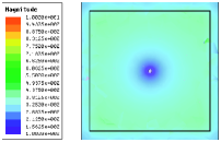
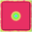
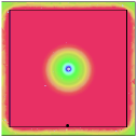
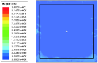
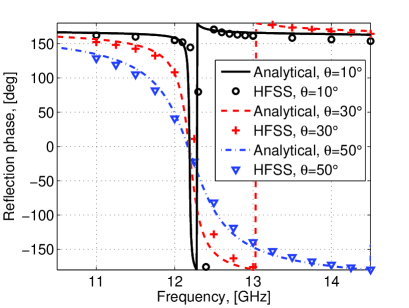
For oblique incidence the wire medium is excited by incident plane waves. The main result which we obtain using this description of the metasurface is the dramatic reduction of the resonance frequency for oblique incidence starting from very small angles. In Fig. 6(b) the reflection phase for the incidence angles of 10, 30, and 50 degrees calculated using 2 is shown. We see clearly that the surface behaves as a magnetic conductor (reflection phase equals to zero) at approximately GHz for all of the incidence angles because as predicted by 8. The HFSS simulations agree well with our analytical results. However, for the incidence angle of 10 degrees the difference between the analytical and the simulated results is somewhat larger than for more oblique angles. Furthermore, Eq. 18 implies that the electric fields inside the wire medium slab are mainly oriented along the metallic vias. Indeed, this can be confirmed by looking at the simulated magnitudes of the normal and transverse components of the electric field shown in Figs. 7 and 8, respectively, for different angles of incidence at 12 GHz. The magnitudes of the electric field components have been plotted at mm above the ground plane. We see also that for the incidence angle of 10 degrees the electric field lines are not as parallel to the metallic vias as they are for the other cases. Because of this, the frequency for which is not exactly that predicted by 18. This explains the larger difference between the analytical and simulated results for the incidence angle of 10 degrees compared to the larger incidence angles in Fig. 6(b).
7 Discussion and conclusions
In this paper we have studied the possibility to use grounded uniaxial materials as magnetic conductors for both TE and TM fields. We have first studied the properties of such surfaces through the derived surface impedance expressions. Attention has been paid especially to the TM polarization which is more promising in view of practical realizations. Based on the results of the theoretical studies we have designed an artificial magnetic conductor having the appearance of a Sievenpiper mushroom structure based on wire-medium slab, but operating in a different regime. The epsilon-near-zero resonance which we use here to create the magnetic conductor effect takes place at a frequency which is approximately twice as lower as the resonant frequency of the same structure at the conventional parallel resonance. This offers a possibility for significant reduction of the layer thickness or for a dual-frequency design, as proposed in [28]. The magnetic wall effect is very little affected by the incidence angle (excluding ). We have verified our results with simulations.
The present study of the properties of grounded uniaxial materials relates closely to the recent studies on the electromagnetic boundary conditions for anisotropic metamaterials [29, 30], where instead of treating the transversal components of the incident fields, the authors propose boundary conditions for the normal components of the incident fields. In [29, 30] the authors arrive to the same conclusion as the results of this paper, that the perfect magnetic boundary condition can be achieved for the TM field by having . In the present paper this is proposed to realize with wire medium at its plasma frequency. It is clear that this boundary condition differs considerable from the conventional boundary condition for the perfect magnetic conductors .
The magnetic wall effect realized for the TM-polarization using the wire medium is limited to the vicinity of the plasma frequency of the wire medium. Because of this, the bandwidth of the magnetic wall effect is small, especially for small incidence angles. However, in some applications, such as GPS or GALILEO, this does not impose any limitations as the needed frequency band for these applications is rather small. In other applications the proposed novel way of realizing the surface resonance can be used to create a secondary resonance in the vicinity of the primary resonance [28]. Also, the surface does not operate as an AMC for the normal incidence. In a practical environment this should not be a problem as the waves impinging to the surface are seldom just normally oriented. Further, in AMC antenna applications, where the primary radiator lies very close to the AMC surface, most of the power from the primary radiator is radiated in the angular spectrum practically excluding the normal incidence.
Acknowledgements
The discussions with Prof. Igor Nefedov are warmly acknowledged. Olli Luukkonen wishes to thank the Nokia Foundation, Jenny and Antti Wihuri Foundation, Emil Aaltonen Foundation, and the Finnish Society of Electronics Engineers for financial support.
References
- [1] D. Sievenpiper, L. Zhang, R. F. J. Broas, N. G. Alexopoulos, and E. Yablonovich, “High-impedance electromagnetic surfaces with a forbidden frequency band,” IEEE Trans. Microwave Theory Tech., Vol. 47, pp. 2059–2074, 1999.
- [2] A. Monorchio, G. Manara, and L. Lanuzza, “Synthesis of artificial magnetic conductors by using multilayered frequency selective surfaces,” IEEE Antennas and Wireless Propagation Letters, Vol. 1, Issue 11, pp. 196–199, 2002.
- [3] S. Clavijo, R. E. Díaz, and W. E. McKinzie, III, “High-impedance surfaces: An artificial magnetic conductor for a positive gain electrically small antennas,” IEEE Trans. Antennas Propagat., Vol. 51, No. 10, pp. 2678–2690, 2003.
- [4] D. J. Kern, D. H. Werner, A. Monorchio, L. Lanuzza, and M. J. Wilhelm, “The design synthesis of multiband artificial magnetic conductors using high impedance frequency selective surfaces,” IEEE Trans. Antennas Propagat., Vol. 53, No. 1, pp. 8–17, 2005.
- [5] A. P. Feresidis, G. Goussetis, W. Shenhong, and J. C. Vardaxoglou, “Artificial magnetic conductor surfaces and their application to low-profile high-gain planar antennas,” IEEE Trans. Antennas Propagat., Vol. 53, No. 1, pp. 209–215, 2005.
- [6] C. R. Simovski, P. de Maagt, and I. V. Melchakova, “High-impedance surface having stable resonance with respect to polarization and incidence angle,” IEEE Trans. Antennas Prop., Vol. 53, No 3, pp. 454–460, 2005.
- [7] G. Goussettis, A. P. Feresidis, and J. C. Vardaxoglou, “Tailoring the AMC and EBG characteristics of periodic metallic arrays printed on grounded dielectric substrate,” IEEE Trans. Antennas Propag., Vol. 54, No. 1, pp. 82–89, 2006.
- [8] O. Luukkonen, C. Simovski, G. Granet, G. Goussetis, D. Lioubtchenko, A. V. Räisänen, and S. A. Tretyakov, “Simple and accurate analytical model of planar grids and high-impedance surfaces comprising metal strips or patches,” IEEE Trans. Antennas Propagat., Vol. 56, No. 6, pp. 1624–1632, June 2008.
- [9] O. Luukkonen, C. Simovski, A. V. Räisänen, and S. A. Tretyakov, “An efficient and simple analytical model for analysis of propagation properties in impedance waveguides,” IEEE Trans. Microw. Theory Tech., Vol. 56, No. 7, pp. 1624–1632, July 2008.
- [10] P.-S. Kildal, “Artificially soft and hard surfaces in electromagnetics,” IEEE Trans. Antennas Propagat., Vol. 38, No. 10, pp. 1537 1544, Oct. 1990.
- [11] R. W. Ziolkowski and A. D. Kipple, “Application of double negative materials to increase the power radiated by electrically small antennas,” IEEE Trans. Antennas Propag., Vol. 51, No. 10, pp. 2626- 2640, 2003.
- [12] A. Erentok, P. L. Luljak, and R. W. Ziolkowski, “Characterization of a volumetric metamaterial realization of an artificial magnetic conductor for antenna applications,” IEEE Trans. Antennas Propagat., Vol. 53, No. 1, pp. 160–172, 2005.
- [13] M. Hirvonen, and J. C.-E. Sten, “Power and of a horizontal dipole over a metamaterial coated conducting surface,” IEEE Trans. Antennas Propagat., Vol. 56, No. 3, pp. 684–690, 2008.
- [14] M. Hirvonen and S. A. Tretyakov, “Near-zero permittivity substrates for horizontal antennas: Performance enhancement and limitations,” Microw. and Optical Techn. Lett., Vol. 50, No. 10, pp. 2674-2677, 2008.
- [15] A. Sihvola, S. Tretyakov, and A. de Baas, Metamaterials with extreme material parameters, Journal of Communications Technology and Electronics, Vol. 52, No. 9, pp. 986 990, 2007.
- [16] S. A. Tretyakov, Analytical Modeling in Applied Electromagnetics, Artech House: Norwood, MA, 2003.
- [17] P. Ikonen, M. Lapine, I. Nefedov, and S. Tretyakov, “Vector circuit theory for spatially dispersive uniaxial magneto-dielectric slabs,” Progress In Electromagnetics Research, PIER 63, pp. 279–294, 2006.
- [18] R. J. King, D. V. Thiel, and K. S. Park, “The synthesis of surface reactance using an artificial dielectric,” IEEE Trans. Antennas Propag., Vol. 31, No. 3, pp. 471–476, May 1983.
- [19] M. G. Silveirinha, C. A. Fernandes, and J. R. Costa, “Electromagnetic characterization of textured surfaces formed by metallic pins,” IEEE Trans. Antennas Propag., Vol. 56, No. 2, pp. 405–415, Feb. 2008.
- [20] G. Shvets, Photonic approach to making a surface wave accelerator, AIP Conference Proceedings, Vol. 647, 371, 2002.
- [21] P. A. Belov, R. Marqués, S. I. Maslovski, I. S. Nefedov, M. Silveirinha, C. R. Simovski, and S. A. Tretyakov, “Strong spatial dispersion in wire media in the very large wavelength limit,” Physical Review B, Vol. 67, 113103, 2003.
- [22] C. R. Simovski, and P. Belov, “Low-frequency spatial dispersion in wire medium,” Physical Review E, Vol. 70, 046616, 2004.
- [23] A. Demetriadou and J. Pendry, “Taming spatial dispersion in wire metamaterial,” J. Phys.: Condens. Matter, Vol. 20, 2008, 295222.
- [24] A. B. Yakovlev, O. Luukkonen, C. R. Simovski, S. A. Tretyakov, S. Paulotto, P. Baccarelli, and G. W. Hanson, “Analytical modeling of surface waves on high impedance surfaces,”Metamaterials and Plasmonics: Fundamentals, Modelling, Applications (Eds. S. Zouhdi, A. Sihvola, and A. P. Vinogradov), NATO Science for Peace and Security Series B, pp. 239–254, 2009.
- [25] O. Luukkonen, M. G. Silveirinha, A. B. Yakovlev, C. R. Simovski, I. S. Nefedov, and S. A. Tretyakov, “Homogenization models for the analysis of reflection properties of mushroom structures,” Proc. 2nd International Congress on Advanced Electromagnetic Materials in Microwaves and Optics, Pamplona, Spain, September 21–26, pp. 208–210, 2008.
- [26] A. B. Yakovlev, M. G. Silveirinha, O. Luukkonen, C. R. Simovski, I. S. Nefedov, and S. A. Tretyakov, “Homogenization models for the analysis of surface waves on analysis of surface waves on mushroom structures” Proc. 2nd International Congress on Advanced Electromagnetic Materials in Microwaves and Optics, Pamplona, Spain, September 21–26, pp. 310–312, 2008.
- [27] Ansoft’s homepage: http://www.ansoft.com/
- [28] O. Luukkonen, F. Costa, A. Monorchio, and S. Tretyakov, “A thin electromagnetic absorber for wide incidence angles and both polarizations”, to appear in IEEE Trans. Antennas Propag., preprint available at http://arxiv.org/abs/0807.4831v3.
- [29] I. V. Lindell and A. H. Sihvola, “Electromagnetic boundary and its realization with anisotropic metamaterial,” Physical Review E, Vol. 79, 026604, 2009.
- [30] I. V. Lindell and A. H. Sihvola, “Uniaxial IB-medium interface and novel boundary conditions,” to appear in IEEE Trans. Antennas Propag..