Spin-injection Hall effect in a planar photovoltaic cell
pacs:
75.50.Pp, 81.05.Ea, 85.75.HhSuccessful incorporation of the spin degree of freedom in semiconductor technology requires the development of a new paradigm allowing for a scalable, non-destructive electrical detection of the spin-polarization of injected charge carriers as they propagate along the semiconducting channel. In this paper we report the observation of a spin-injection Hall effect (SIHE) which exploits the quantum-relativistic nature of spin-charge transport and which meets all these key requirements on the spin detection. The two-dimensional electron-hole gas photo-voltaic cell we designed to observe the SIHE allows us to develop a quantitative microscopic theory of the phenomenon and to demonstrate its direct application in optoelectronics. We report an experimental realization of a non-magnetic spin-photovoltaicZutic:2001_a effect via the SIHE, rendering our device an electrical polarimeter which directly converts the degree of circular polarization of light to a voltage signal.Ganichev:2001_a
Magneto-optical imagingKikkawa:1999_a ; Crooker:2005_a ; Weber:2006_a ; Lou:2007_a of electron spins is an established qualitative probe which, although non-destructive, does not currently offer a sub-micron resolution and the possibility to integrate the probe within a semiconductor device. Methods introduced to date that allow for such an integration are destructive. One is based on extracting the spin-polarized current by a ferromagnetHammar:2002_a ; Lou:2007_a and this implies further complications stemming from the semiconductor-magnet hybrid design. The other method is based on radiative electron-hole recombinationFiederling:1999_a ; Ohno:1999_b ; Zhu:2001_a ; Jiang:2005_b and here an additional device is needed to convert the emitted circularly polarized light into an electrical signal. The SIHE we introduce in our work is a transverse voltage response to the local spin-polarization of injected charge carriers. Its physical origin is related to the anomalous Hall effect (AHE) in uniformly polarized systems,Chazalviel:1975_a ; Ohno:1992_a ; Cumings:2006_a ; Miah:2007_a i.e. is due to the spin-orbit coupling effects on electrical transport, but unlike the AHE is observed outside the area in which spin-polarization is generated and is spatially non-uniform. The SIHE is also distinct from the (inverse) spin Hall effectsKato:2004_d ; Wunderlich:2004_a ; Valenzuela:2006_a which are based on the subtle concept of pure spin-currents.Sinova:2005_b We demonstrate in this paper that the SIHE is a non-destructive local probe embedded directly along the semiconducting channel, operates without external magnetic fields or magnetic elements introduced in the structure, and has the resolution given by the state-of-the-art semiconductor processing limits. These experimental results combined with a detailed microscopic theory picture of the SIHE we provide imply broad implications of the effect for basic physics research and applications in the area of spin-charge dynamics phenomena.
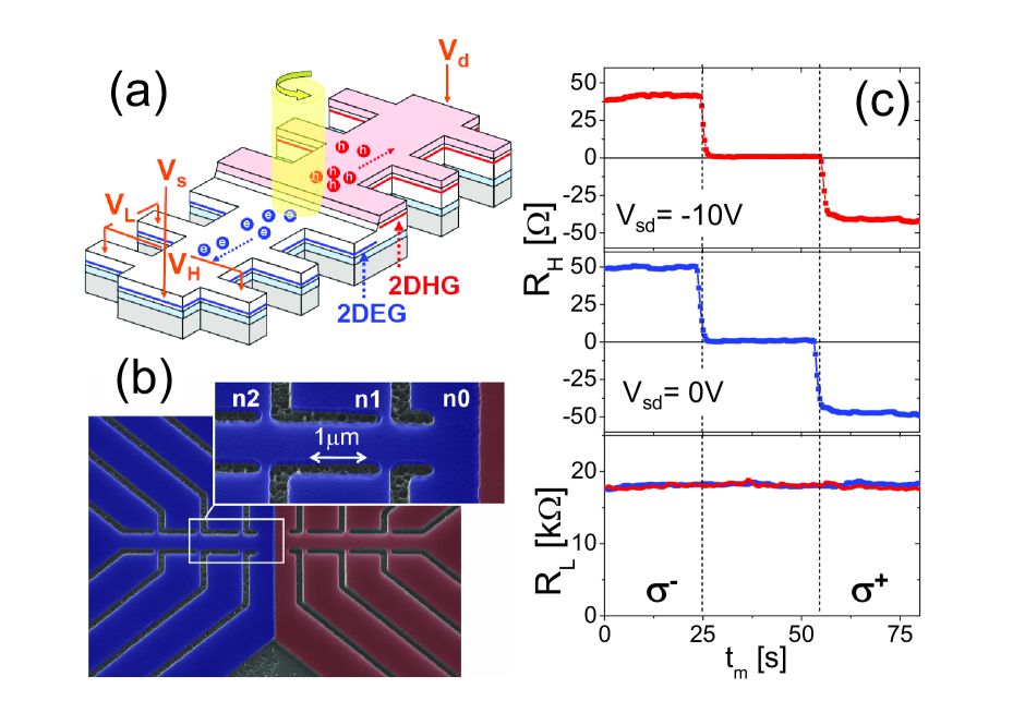
The design of the all-semiconductor SIHE microchips utilized in our study combines conventional approaches to semiconductor device fabrication with processing steps dictated by the special requirements on the electrical spin detection. Molecular-beam epitaxy grown (Al,Ga)As/GaAs heterostructure is the starting semiconductor material, chosen for its well established optical generation of spin-polarized electron-hole pairs. The requirements to spatially separate electrons and holes and to inject the respective spin-polarized currents into thin Hall bar channels led us to utilize a co-planar two-dimensional electron-hole gas (2DEG-2DHG) p-n junction, illustrated schematically in Fig. 1(a). The wafer, grown along the [001]-axis, consists of a modulation p-doped AlGaAs/GaAs heterojunction on top of the structure separated by 90 nm of intrinsic GaAs from an n-doped AlGaAs/GaAs heterojunction underneath (for further details see ”wafer 2” in Ref. Kaestner:2004_thesis, and Supplemetary material). In the unetched part of the wafer the top heterojunction is populated by the 2DHG while the 2DEG at the bottom heterojunction is depleted. The n-side of the co-planar p-n junction is formed by removing the p-doped surface layer from a part of the wafer which results in populating the 2DEG. The corresponding 2D electron density is 2.5 cm-2 with mobility cm2/Vs.
Detailed numerical simulationsKaestner:2004_thesis of the structure show that the lateral extent of the depletion layer at the p-n junction and of the corresponding built-in potential is approximately 100 nm. This sets the upper limit on the width of the optical generation region of counter-propagating electron and hole currents at zero bias. Measurements with variable position of the m laser spot at reverse bias and sub-gap wavelengths used in the experiments confirmed negligible photo-generation inside the 2DEG channel, certainly beyond a distance of 1 m from the p-n junction. (Note that the Stark effect allows for sub-gap excitations from or to the confined 2D states near the p-n junction due to the strong build in electric field.Wunderlich:2004_a ) In all measurements presented below, the 2DEG Hall probes n1-n3, placed at distances of 1.5, 3.5, and 5.5 m from the p-n junction along the 1 m wide [10]-oriented Hall bar, are therefore outside the optical spin-generation area.
The spin-orbit coupling length in our 2DEG, discussed in detail in the theory section below, is of a micrometer scale. In order to provide local detection of the spin-polarization, the width of the Hall contacts has to be therefore substantially smaller than a micrometer. We have optimized the electron-beam lithography and reactive ion etching procedures for our co-planar p-n junction wafer to achieve contact widths of approximately 100 nm, as shown in the scanning electron micrograph in Fig. 1(b). To guarantee proper alignment throughout all fabrication steps, the probe n0 placed next to the p-n junction is wider (750 nm) and can overlap with the spin-generation area. Voltages detected at this probe are interpreted as a combination of the AHE and of an averaged SIHE signal. For reference measurements, additional Hall probes were placed symmetrically in the 2DHG whose typical spin-orbit and spin-coherence lengths are below the limits of the state-of-the-art lithography. We have studied five devices fabricated from the wafer all showing reproducible SIHE characteristics.
Typical SIHE signals in the 2DEG (with the laser spot focused on the p-n junction) are demonstrated in Fig. 1(c) for probe n2. Using a linear polarizer and a wave-plate we prepare in step 1 a linearly polarized light beam at +45∘ angle with respect to the optical axis of a photo-elastic modulator (PEM). The PEM retardation is set to oscillate between , producing a circularly polarized light with oscillating helicity. Hall voltages are measured by recording the amplitude and phase of the signal from a lock-in amplifier with a reference frequency of the retardation oscillation of the PEM. In step 2, the PEM retardation is set to and in the middle of this measurement we manually rotate the wave-plate so that the incoming linearly polarized light beam is at -45∘ angle with respect to the optical axis of the PEM. In step 3, the PEM retardation is reset to its state in step 1, i.e., the left and right circular polarizations of the beam incident on the sample switched places compared to step 1 (for further details on the experimemtal technique see Supplementary material). While the longitudinal resistance is insensitive to the polarization of the incident light, the Hall signals are antisymmetric with respect to the helicity of the circular polarization. Due to the optical selection rules, the spin-polarization of the injected carriers is determined by the polarization of the incident light, i.e., the sign of the Hall signal we observe reverses upon reversing the out-of-plane spin-polarization of the optically generated conduction electrons. In the theory section we show that depending on the local out-of-plane component of their spin the electrons are asymmetrically deflected towards the edges of the 2DEG channel due to spin-orbit coupling, creating a finite Hall voltage. The observation of the Hall signals at zero bias at probe n2 and the similarity between data at zero and -10 V bias confirm, as explained above, that Hall signals in these experiments are detected away from the generation area, i.e., we measure the SIHE.
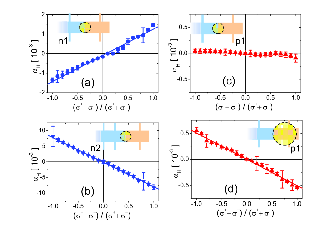
Detailed dependencies of the SIHE at probes n1 and n2 on the degree of circular polarization of the incident light, as modulated by the PEM, are presented in Fig. 2(a) and (b). Here we plot the Hall angles determined as the ratio between longitudinal sheet resistance, measured between successive Hall contacts, and transverse resistances. The SIHE signals are linear in the degree of polarization which is analogous to the proportionality of the AHE to the magnetization in uniformly polarized systems. We also point out the large magnitude of the SIHE. The Hall angles we observe are comparable to anomalous Hall angles in metal ferromagnets.
In Fig. 2(c) and (d) we present Hall measurements in the 2DHG. We compare signals acquired with the laser spot focused on the p-n junction as in the case of the SIHE measurements in the 2DEG, and then moved towards the first 2DHG Hall probe next to the p-n junction and defocused. Consistent with the small spin coherence length in the strongly spin-orbit coupled 2DHG, no clearly measurable SIHE is found with the laser spot focused on the p-n junction. We observe, however, a strong transverse-voltage signal when uniformly polarizing a larger area of the 2DHG around the Hall probe. This measurement links our work to previous studies of the AHE in homogeneously polarized semiconductorsChazalviel:1975_a ; Ohno:1992_a ; Cumings:2006_a ; Miah:2007_a and emphasizes the distinction between the AHE and SIHE. Unlike the AHE, the SIHE probes the spin of carriers outside the region subject to fields which generate spin-polarization.
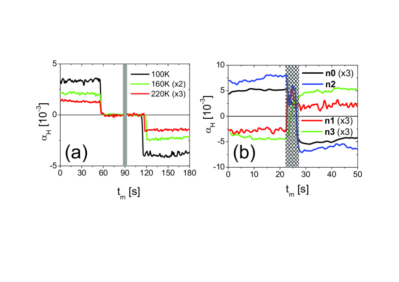
Fig. 3(a) shows the SIHE measured at the 2DEG probe n2 at 100, 160, and 220 K (at temperatures where the p-n junction leakage current is still negligible), demonstrating that the effect is readily detectable at high temperatures. Together with the zero-bias operation demonstrated in Fig. 1(c) and linearity in the degree of circular polarization of the incident light shown in Fig. 2, these characteristics represent the realization of the spin-photovoltaic effect in a non-magnetic structure and demonstrate the utility of the device as an electrical polarimeter. Note that our approach is distinct from the former proposal of the spin-voltaic effect which assumes different longitudinal transport coefficients for spin-up and spin-down channels due to a non-zero equilibrium spin-polarization in the system.Zutic:2001_a ; Kondo:2006_a
In Fig. 3(b) we plot simultaneously the Hall signals measured in all available 2DEG probes. As an experimental consistency check, we skipped the measurement step 2 when acquiring these data. The manual rotation of the wave-plate, causing a continuous rotation of the polarization angle of the incoming beam from +45∘ to -45∘ with respect to the optical axis of the PEM, was performed with fixed PEM retardation setting. The observed Hall signals again change sign for reversed helicities of the incident light. The data in Fig. 3(b) underline the capability of the SIHE to detect locally spin-polarization of injected electrical currents, which in general can be non-uniform along the conducting channel. Signals of one sign, for a given helicity of the incident light, are observed at probes n0 and n2 and signals of opposite sign are detected at probes n1 and n3. Recall that the probe n0 covers a relatively large area which together with the non-uniformity of the spin polarization explains smaller voltage measured at this probe compared to probe n2, despite the immediate vicinity of probe n0 to the p-n junction. The alternation of the sign of simultaneously detected SIHE signals (see also Figs. 2(a) and (b)) is another experimental observation which allows us to exclude spurious origin of the measured voltages. It also points towards the utility of the SIHE in the research of coupled charge and spin dynamics of carriers injected into non-magnetic systemsSchliemann:2003_c ; Bernevig:2006_a ; Weber:2006_a and of the related spintronic device concepts.Datta:1990_a ; Ohno:2008_a These studies are, however, beyond the scope of our initial report of the SIHE. In the remaining paragraphs we keep the focus on the effect itself and establish our interpretation of the measured Hall signals by developing a semi-quantitative microscopic theory of the SIHE assuming parameters of the experimental system.
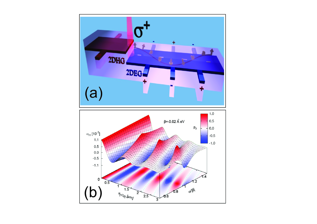
Our theoretical approach is based on the observation that the micrometer length scale governing the spatial dependence of the non-equilibrium spin-polarization is much larger than the nm mean-free-path in our 2DEG which governs the transport coefficients. This allows us to first calculate the steady-state spin-polarization profile along the channel and then consider the SIHE as a response to the local out-of-plane component of the polarization, as illustrated schamatically in Fig. 4(a) (see also Supplementary material for detailed theory derivations). The calculations start from the electronic structure of GaAs whose conduction band near the -point is formed dominantly by Ga -orbitals. This implies weak spin-orbit coupling originating from the mixing of the valence-band -orbitals and from the broken inversion symmetry in the zincblende lattice. In the presence of an electric potential the corresponding 3D spin-orbit coupling Hamiltonian reads
| (1) |
where are the Pauli spin matrices, is the momentum of the electron, eVÅ3 , and Å2 for GaAs.Knap:1996_a ; Winkler:2003_a Eq. (1) together with the 2DEG confinement yield an effective 2D Rashba and Dresselhaus spin-orbit coupled Hamiltonian,Schliemann:2003_c ; Bernevig:2006_a
| (2) |
where , eVÅ and eVÅ for the strength of the confining electric field, eV/Å , obtained from a self-consistent Poisson-Schrödinger simulation of the conduction band profile of our GaAs/AlGaAs heterostructure.Kaestner:2004_thesis ; Wunderlich:2004_a
In the weak spin-orbit coupling regime of our structure with and (0.5 meV) much smaller than the disorder scattering rate (5 meV), the system obeys a set of spin-charge diffusion equations.Bernevig:2006_a In the steady-state we obtain that the spatial dependence of the out-of-plane component of the spin polarization along the [10] channel direction is given by a damped oscillatory function with the complex wavevector , where , , and .
From the known local spin-polarization we calculate the Hall signal by realizing that the dominant contribution in the weak spin-orbit coupling regime is the extrinsic skew-scattering. This contribution is obtained by considering asymmetric scattering from a spin-orbit coupled impurity potential originating from the first term in Eq. (1).Nozieres:1973_a ; Crepieux:2001_b Within the second-order Born approximation for short-range scatterers we obtain the spatially dependent SIHE angle,Nozieres:1973_a ; Crepieux:2001_b
| (3) |
where is the density of optically injected carriers into the 2DEG channel. In Fig. 4(b) we plot the resulting theoretical along the [10] direction for the relevant range of Rashba and Dresselhaus parameters corresponding to our experimental structure. We have assumed a donor impurity density of the order of the equilibrium density of the 2DEG in dark, which is an upper bound for the strength of the impurity scattering in our modulation-doped heterostructure and, therefore, a lower bound for the Hall angle. For the mobility of the injected electrons in the 2DEG channel we considered the experimental value determined from ordinary Hall measurements without illumination. The density of photoexcited carriers of cm-2 was obtained from the measured longitudinal resistance between successive Hall probes under illumination assuming constant mobility.
The theory results shown in Fig. 4(b) provide a semi-quantitative account of the magnitude of the observed SIHE angle () and explain the linear dependence of the SIHE on the degree of spin-polarization of injected carriers. The calculations are also consistent with the experimentally inferred precession length of the order of a micrometer and the spin-coherence exceeding micrometer length scales. We emphasize that the 2DEG in the strong disorder, weak spin-orbit coupling regime realized in our experimental structures is a particularly favorable system for theoretically establishing the presence of the SIHE. In this regime and for the simple band structure of the archetypal 2DEG, the spin-diffusion equations and the leading skew-scattering mechanism of the spin-orbit coupling induced Hall effect are well understood areas of the physics of quantum-relativistic spin-charge dynamics. The possibility to observe the SIHE in normal semiconductors, established in our work, and to tune independently the strengths of disorder and spin-orbit coupling in semiconductor structures open new opportunities for resolving long-standing debates on the nature of spin-charge dynamics in the intriguing strong spin-orbit coupling regime. Apart from these basic physics problems, the SIHE can be directly implemented in devices such as the spin-photovoltaic cell demonstrated in this paper, in the Datta-DasDatta:1990_a and related semiconductor spintronic transistors, and in a number of other microelectronic devices utilizing the spin degree of freedom of charge carriers.
We acknowledge support from EU Grant IST-015728, from Czech Republic Grants FON/06/E001, FON/06/E002, AV0Z10100521, KAN400100652, LC510, and Preamium Academiae, and from U.S. Grants ONR-N000140610122, DMR-0547875, and SWAN-NRI. Jairo Sinova is a Cottrell Scholar of Research Corporation.
References
- (1) Zutic, I., Fabian, J., and Sarma, S. D. Phys. Rev. Lett. 88, 066603 (2002).
- (2) Ganichev, S. D., Ivchenko, E. L., Danilov, S. N., Eroms, J., Wegscheider, W., Weiss, D., and Prettl, W. Phys. Rev. Lett. 86, 4358 (2001).
- (3) Kikkawa, J. M. and Awschalom, D. D. Nature 397, 139 (1999).
- (4) Crooker, S. A., Furis, M., Lou, X., Adelmann, C., Smith, D. L., Palmstrøm, C. J., and Crowell, P. A. Science 309, 2191 (2005).
- (5) Weber, C. P., Orenstein, J., Bernevig, B. A., Zhang, S.-C., Stephens, J., and Awschalom, D. D. Phys. Rev. Lett. 98, 076604 (2007).
- (6) Lou, X., Adelmann, C., Crooker, S. A., Garlid, E. S., Zhang, J., Reddy, S. M., Flexner, S. D., Palmstrom, C. J., and Crowell, P. A. Nature Physics 3, 197 (2007).
- (7) Hammar, P. R. and Johnson, M. Phys. Rev. Lett. 88, 066806 (2002).
- (8) Fiederling, R., Keim, M., Reuscher, G., Ossau, W., Schmidt, G., Waag, A., and Molenkamp, L. W. Nature 402, 787 (1999).
- (9) Ohno, Y., Young, D. K., Beschoten, B., Matsukura, F., Ohno, H., and Awschalom, D. D. Nature 402, 790 (1999).
- (10) Zhu, H. J., Ramsteiner, M., Kostial, H., Wassermeier, M., Schönherr, H. P., and Ploog, K. H. Phys. Rev. Lett. 87, 016601 (2001).
- (11) Jiang, X., Wang, R., Shelby, R. M., Macfarlane, R. M., Bank, S. R., Harris, J. S., and Parkin, S. S. P. Phys. Rev. Lett. 94, 056601 (2005).
- (12) Chazalviel, J. N. Phys. Rev. B 11, 3918 (1975).
- (13) Ohno, H., Munekata, H., Penney, T., von Molnár, S., and Chang, L. L. Phys. Rev. Lett. 68, 2664 (1992).
- (14) Cumings, J., Moore, L. S., Chou, H. T., Ku, K. C., Xiang, G., Crooker, S. A., Samarth, N., and Goldhaber-Gordon, D. Phys. Rev. Lett. 96, 196404 (2006).
- (15) Miah, M. I. J. Phys. D: Appl. Phys 40, 1659 (2007).
- (16) Kato, Y. K., Myers, R. C., Gossard, A. C., and Awschalom, D. D. Science 306, 1910 (2004).
- (17) Wunderlich, J., Kaestner, B., Sinova, J., and Jungwirth, T. Phys. Rev. Lett. 94, 047204 (2005).
- (18) Valenzuela, S. O. and Tinkham, M. Nature 442, 176 (2006).
- (19) Sinova, J., Murakami, S., Shen, S.-Q., and Choi, M.-S. Solid State Commun. 138, 214 (2006).
- (20) B. Kaestner, D. G. Hasko, D. A. Williams, (Thesis) Design of quasi-lateral p-n junction for optical spin-detection in low-dimensional systems , (2004), preprint arXiv:cond-mat/0411130.
- (21) Kondo, T., ji Hayafuji, J., and Munekata, H. J. J. Appl. Phys. 45, L663 (2006).
- (22) Schliemann, J., Egues, J. C., and Loss, D. Phys. Rev. Lett. 90, 146801 (2003).
- (23) Bernevig, B. A., Orenstein, J., and Zhang, S.-C. Phys. Rev. Lett. 97, 236601 (2006).
- (24) Datta, S. and Das, B. Appl. Phys. Lett. 56, 665 (1990).
- (25) Ohno, M. and Yoh, K. Phys. Rev. B 77, 045323 (2008).
- (26) Knap, W., Skierbiszewski, C., Zduniak, A., Litwin-Staszewska, E., Bertho, D., Kobbi, F., Robert, J. L., Pikus, G. E., Pikus, F. G., Iordanskii, S. V., Mosser, V., Zekentes, K., and Lyanda-Geller, Y. B. Phys. Rev. B 53 (1996).
- (27) Winkler, R. Spin-Orbit Coupling Effects in Two-Dimensional Electron and Hole Systems. Spinger-Verlag, New York, (2003).
- (28) Nozieres, P. and Lewiner, C. J. Phys. France 34, 901 (1973).
- (29) Crépieux, A. and Bruno, P. Phys. Rev. B 64, 014416 (2001).
- (30) Kovalev, A. A., Výborný, K., and Sinova, J. Phys. Rev. B 78, 041305 (2008).
- (31) Borunda, M., Nunner, T. S., Luck, T., Sinitsyn, N. A., Timm, C., Wunderlich, J., Jungwirth, T., MacDonald, A. H., and Sinova, J. Phys. Rev. Lett. 99, 066604 (2007).
- (32) Nunner, T. S., Sinitsyn, N. A., Borunda, M. F., Dugaev, V. K., Kovalev, A. A., Abanov, A., Timm, C., Jungwirth, T., ichiro Inoue, J., MacDonald, A. H., and Sinova, J. Phys. Rev. B 76, 235312 (2007).
- (33) Onoda, S., Sugimoto, N., and Nagaosa, N. Phys. Rev. B 77, 165103 (2008).
- (34) For comparison with the cited references, in Ref. Nozieres:1973_a and in Ref. Crepieux:2001_b and the results translated to two-dimensions. The assumed disorder potential is uncorrelated delta scatterers with a density .