N,N’-dimethylperylene-3,4,9,10-bis(dicarboximide) on alkali halide(001) surfaces
Abstract
The growth of N,N’-dimethylperylene-3,4,9,10-bis(dicarboximide) (DiMe-PTCDI) on KBr(001) and NaCl(001) surfaces has been studied. Experimental results have been achieved using frequency modulation atomic force microscopy at room temperature under ultra-high vacuum conditions. On both substrates, DiMe-PTCDI forms molecular wires with a width of 10 nm, typically, and a length of up to 600 nm at low coverages. All wires grow along the [110] direction (or [10] direction, respectively) of the alkali halide (001) substrates. There is no wetting layer of molecules: Atomic resolution of the substrates can be achieved between the wires. The wires are mobile on KBr surface but substantially more stable on NaCl. A p(2 x 2) superstructure in brickwall arrangement on the ionic crystal surfaces is proposed based on electrostatic considerations. Calculations and Monte-Carlo simulations using empirical potentials reveal possible growth mechanisms for molecules within the first layer for both substrates, also showing a significantly higher binding energy for NaCl(001). For KBr, the p(2 x 2) superstructure is confirmed by the simulations, for NaCl, a less dense, incommensurate superstructure is predicted.
pacs:
68.37.Ps, 61.64.+w, 68.55.AcI Introduction
The possible use of organic molecules for advanced types of electronic devices has attracted much interest in recent decades.Dimitrakopoulos and Malenfant (2002); Horowitz (1998); Jäckel et al. (2004) A large field of research has emerged, studying the structural and electronic properties of various molecules on solid surfaces. Scanning probe methods have proved to be a powerful tool for these studies, especially scanning tunneling microscopy (STM) has been used for many promising studies.Moresco et al. (2001); Temirov et al. (2006); Liljeroth et al. (2007) Nevertheless, STM is limited to conducting surfaces, while insulating surfaces are still important: Here, the influence of the substrate on the electronic properties is small compared to metal or semiconductor surfaces.
Frequency modulation atomic force microscopy (FM-AFM)Albrecht et al. (1991); Giessibl (1995) is a scanning probe technique that allows for real space imaging of insulating surfaces. Thus it has made the analysis of the structural properties of organic molecules on insulators accessible.Nony et al. (2004a, b) Recent studies demonstrate the capability of the technique to analyse the growth of the prototypical semiconductor molecules C60Burke et al. (2007, 2005) and 3,4,9,10-perylene-tetracarboxylic-dianhydride (PTCDA)Fendrich et al. (2007); Kunstmann et al. (2005); Mativetsky et al. (2007); Dienel et al. (2008); Burke et al. (2008) on alkali halide (001) surfaces.
However, all these studies show dewetting of the surfaces and the growth of bulk-like molecular structures for PTCDA or fractal islands for C60. For the development of small-scale electronic devices, a controlled growth of low-dimensional molecular structures would be desirable.Schnadt et al. (2008) This kind of growth has recently been analysed for a perylene derivate similar to PTCDA, N,N’-dimethylperylene-3,4,9,10-bis(dicarboximide) (DiMe-PTCDI); Gavrila et al. (2004); Hädicke and Graser (1986); Schäfer et al. (2001, 1998) this molecule shows the growth of wire-like structures on KBr(001).Fendrich and Kunstmann (2007)
The present paper reviews the results for KBr(001) and shows experimental data for another alkali halide surface, NaCl(001), as well as molecular force field calculations analysing the molecular arrangement of DiMe-PTCDI on both substrates.
II Experimental
The experiments have been performed at room temperature under ultra-high vacuum(UHV) conditions in a commercially available analysis system (AFM/STM by Omicron, Germany) operated in FM-AFM mode. The oscillation of the cantilever is detected by beam deflection; to illuminate the cantilever, a SuperLum LED coupled to the UHV chamber by a single-mode fiber was used. For the detection of the frequency and control of the cantilever oscillation amplitude, we used the easyPLLplus system (Nanosurf, Switzerland), operating in self oscillation mode. The specifications of the silicon cantilevers (PPP-NCL by Nanosensors, Switzerland) were: resonant frequencies of kHz, spring constants of 30 - 40 N/m and quality factors of 30000 in UHV. The cantilevers were driven at an amplitude of nm, typically. In some experiments, a voltage between tip and sample was applied to compensate for electrostatic interactions. Specific frequency shifts are given for each image.
For scanning control and data acquistion, the open-source software GXSMZahl et al. (2003) combined with home-built electronics has been used. Image processing has been done using the free software WSXM.Horcas et al. (2007)
Clean KBr and NaCl (001) surfaces have been prepared by in situ cleaving of commercially available single crystals (Korth, Germany). The crystals have been heated at 450 K for 1 h before cleaving to remove contaminations and also after cleaving to remove trapped charges. After preparation of the substrates, various amounts of DiMe-PTCDI have been evaporated onto the samples from a home-built crucible. The temperature of the oven was 550 K, the evaporation rate was checked before and after deposition by a quadrupole mass spectrometer. During evaporation, the sample was kept at room temperature.
III Experimental results
III.1 KBr(001)
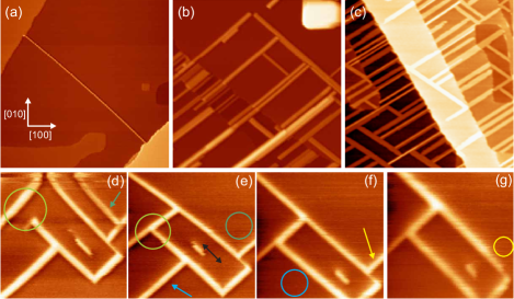
On KBr(001) surfaces, DiMe-PTCDI grows wire-like islands with a length of up to 600 nm (see Fig. 1). Between the wires, atomic resolution of the KBr substrate could be achieved: There is no wetting layer of organic molecules. All wires are aligned with surface axes. The wires are stabilized by step edges, ”loose ends” are seldom observed. When no step edges are present, the structures are highly unstable and diffuse when scanned for a longer time. The wires have a height of at least two molecular layers.
Due to their instability, no molecular resolution of the wires was possible, so no information on the arrangement of the molecules within the wire, could be achieved experimentally. For the initial growth, i.e., for the first layer upon the KBr substrate, a model proposing a p(22) superstructure in brickwall arrangement has been elaborated. This model was based on force field calculations and electrostatic considerations for a single molecule on the ionic KBr(001) surface.Fendrich and Kunstmann (2007)
III.2 NaCl(001)
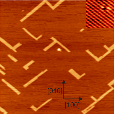
On NaCl(001) surfaces, DiMe-PTCDI molecules show similar structures. As shown in Fig. 2, wires are still aligned with surface axes. No wetting layer of molecules is found. In contrast to KBr, the wires are much more stable, even if they are not stabilized by step edges: The area shown in the image has been scanned for several hours without showing any changes in the arrangement of the molecular islands. All the wires are two molecular layers high.
On KBr, continuous networks of wires have been found, supposably due to stability reasons; here, we find smaller islands that are not interconnected and sometimes consist of several merged perpendicular wires. No step edges are needed as nucleation centers for the islands on NaCl; it seems reasonable that islands nucleate at surface defects.
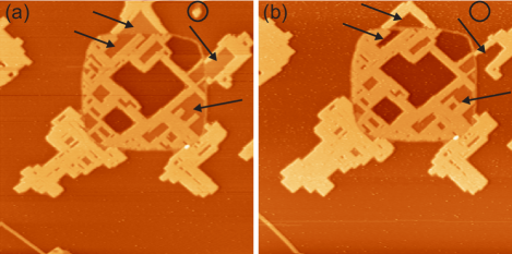
When the coverage of molecules on the surface is increased, larger and more compact molecular islands are found while the framework of the perpendicularly arranged wires can still be seen. Islands with a height of up to 4 molecular layers have been observed. Within these islands, 1-layer areas are embedded; however, these wetting layers are unstable, a dewetting of the 1-layer areas is observed within several minutes. Fig. 3 shows two subsequent scans of the same area (500 500 nm2). One can see the molecules dissappear from the enclosed areas covered with only one layer of molecules. These molecules diffuse two higher layers, as reported also for C60 molecules on KBr(001).Burke et al. (2007, 2005)
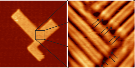
As the islands are wider and more stable than on KBr(001), molecular resolution of the topmost layer of DiMe-PTCDI on NaCl(001) was possible. Fig.4 shows resolution of molecular rows on top of an island which is 2 layers high and merged out of 3 wires. The junction can clearly be seen on the molecular scale as an interface of perpendicular rows. The internal structure of the molecular rows cannot be resolved; nevertheless, every second row seems shorter at the junction, thus a brickwall arrangement of the molecules seems reasonable.
IV Calculations
To get further insight into the growth mechanisms for DiMe-PTCDI on alkali halide (001) surfaces and corrobarate the models based on the experimental findings, molecular force field calculations based on empirical potentials have been performed. The capability of empirical potentials has been shown for several molecular systems.Mannsfeld and Fritz (2004); Mannsfeld et al. (2005); Fendrich et al. (2006); Fendrich and Krug (2007) In particular, similar calculations could elucidate the experimental data for a very similar system, PTCDA on KCl(001).Dienel et al. (2008)
As preliminary calculations, the potential energies of single DiMe-PTCDI molecule on KBr(001) and NaCl(001) have been calculated using the empirical potentials of the AMBER molecular force field.Weiner et al. (1984, 1986); Cornell et al. (1995) As DiMe-PTCDI is a polar molecule (the electronegativity of the 4 oxygen atoms causes a shift of negative charge to the ”corners” of the molecule), the electrostatics of the system have to be accounted for. The polarity of the molecule is represented by partial charges assigned to each atom within the molecule by a Mulliken method, using the software Hyperchem. Each ion of the substrate is represented by a point charge of .
Calculating the potential energy as described above, the minimum energy position for a single molecule was determined for both substrates using a gradient search algorithm. Optimum positions are found as shown in Fig. 5, i.e., on top of a halide ion, the molecule aligned with the [110] axis of the substrate. In this way, the negatively charged oxygen atoms are close to 4 positive alkali ions of the substrate. The adsorption geometry is more favorable for NaCl, which has a smaller lattice constant of 562 pm compared to KBr (658 pm); therefore, the binding energy of a single molecule is higher for NaCl ( = - 1.65 eV, = -1.35 eV).
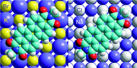
In a second step, potential energies for larger molecular domains have been calculated. The Grid method and the software Powergrid Mannsfeld (2004); Mannsfeld and Fritz (2004) have been used to calculate the potential energy for domains consisting of 150 molecules or more. The molecular arrangement within the domain has been optimized using a Monte-Carlo method, the Metropolis algorithm.Metropolis et al. (1953) Several Monte-Carlo experiments have been performed: After the Metropolis algorithm was started for an arbitrary initial configuration, the arrangement was optimized, i.e. the size of the unit cell and the orientation of the molecules within the unit cell were changed until an optimum arrangement was found. The calculation confirms the supposed p(2 2) brickwall arrangement for one layer of DiMe-PTCDI molecules on KBr(001). For NaCl(001), a incommensurate structure with an epitaxy matrix of
| (3) |
was found. Within the domain, all the molecules are still aligned towards the substrate axis.
The higher stability of the islands on NaCl(001) reflects in a higher binding energy for the domains. The energy per molecule within a domain is = -1.4 eV for KBr and = -1.8 eV for NaCl. Table 1 shows the results of the calculations.
| KBr(001) | NaCl(001) | |
| structure | commensurate | incommensurate |
| p(2 2) | ||
| brickwall | brickwall | |
| area per | A = 1.74 nm2 | A = 1.37 nm2 |
| molecule | ||
| binding energy | -1.35 eV (single) | -1.65 eV(single) |
| per molecule | -1.4 eV (domain) | -1.8 eV (domain) |
V Conclusion
We have shown an experimental study of DiMe-PTCDI on two alkali halide (001) substrates, KBr(001) and NaCl(001). On both substrates, we have observed the growth of wire-like molecular islands which are oriented along the substrate axis. The wires are at least 2 molecular layers high for both substrates. The wires are very mobile on KBr surfaces, where they are stabilized by step edges; on NaCl surfaces, the wires are more stable, allowing for the resolution of molecular rows within the topmost molecular layer. When larger amounts of molecules are evaporated onto NaCl(001) surfaces, large, compact islands are found. In contrast to the two-layer wires at low coverages, monolayer-covered areas are found. However, a dewetting of these areas was observed, possibly induced or supported by the scanning tip.
Calculations based on empirical potentials give further insight to the structural properties. For KBr(001), a p(2 2) superstructure is found, all molecules are aligned towards the substrate axis. This alignment is also found for NaCl(001), however, in this case an incommensurate superstructure is predicted. However, at least this purely theoretical finding has to be doubted, as there are no experimental hints. Inaccuracies of the calculation may occur for several reason: In contrast to the experiment, only one layer of molecules on the substrates is considered; all molecules are lying flat on the surface, a constriction that is necessary for the Grid method;Mannsfeld and Fritz (2004) and possible conformational changes of molecules or substrates are completely neglected, both molecules and substrates are rigid. In spite of the inaccuracies of the calculations, the higher stability for NaCl reflects in a higher binding energy for this substrate compared to KBr.
VI Acknowledgement
Financial support is granted by the Deutsche Foschungsgemeinschaft through SFB616 ”Energy Dissipation at Surfaces”.
References
- Dimitrakopoulos and Malenfant (2002) C. D. Dimitrakopoulos and P. R. L. Malenfant, Adv. Mat. 14, 99 (2002).
- Horowitz (1998) G. Horowitz, Adv. Mat. 10, 365 (1998).
- Jäckel et al. (2004) F. Jäckel, M. D. Watson, K. Mullen, and J. P. Rabe, Phys. Rev. Lett. 92, 188303 (2004).
- Liljeroth et al. (2007) P. Liljeroth, J. Repp, and G. Meyer, Science 317, 1203 (2007).
- Temirov et al. (2006) R. Temirov, S. Soubatch, A. Luican, and F. S. Tautz, Nature 444, 350 (2006), ISSN 0028-0836.
- Moresco et al. (2001) F. Moresco, G. Meyer, K.-H. Rieder, H. Tang, A. Gourdon, and C. Joachim, Phys. Rev. Lett. 86, 672 (2001).
- Albrecht et al. (1991) T. Albrecht, P. Grütter, D. Horne, and D. Rugar, J. Appl. Phys. 69, 668 (1991).
- Giessibl (1995) F. Giessibl, Science 267, 68 (1995).
- Nony et al. (2004a) L. Nony, R. Bennewitz, O. Pfeiffer, E. Gnecco, A. Baratoff, E. Meyer, T. Eguchi, A. Gourdon, and C. Joachim, Nanotechnology 15, S91 (2004a).
- Nony et al. (2004b) L. Nony, E. Gnecco, A. Baratoff, A. Alkauskas, R. Bennewitz, O. Pfeiffer, S. Maier, A. Wetzel, E. Meyer, and C. Gerber, Nano Letters 4, 2185 (2004b).
- Burke et al. (2007) S. A. Burke, J. M. Mativetsky, S. Fostner, and P. Grütter, Phys. Rev. B 76, 035419 (2007).
- Burke et al. (2005) S. Burke, J. Mativetsky, R. Hoffmann, and P. Grütter, Phys. Rev. Lett. 94, 096102 (2005).
- Fendrich et al. (2007) M. Fendrich, T. Kunstmann, D. Paulkowski, and R. Möller, Nanotechnology 18, 084004 (2007).
- Kunstmann et al. (2005) T. Kunstmann, A. Schlarb, M. Fendrich, T. Wagner, R. Möller, and R. Hoffmann, Phys. Rev. B 71, 121403(R) (2005).
- Mativetsky et al. (2007) J. Mativetsky, S. Burke, S. Fostner, and P. Grütter, Nanotechnology 18, 105303 (2007).
- Dienel et al. (2008) T. Dienel, C. Loppacher, S. Mannsfeld, R. Forker, and T. Fritz, Adv. Mat. 20, 959 (2008).
- Burke et al. (2008) S. A. Burke, W. Ji, J. M. Mativetsky, J. M. Topple, S. Fostner, H.-J. Gao, H. Guo, and P. Grutter, Phys. Rev. Lett. 100, 186104 (pages 4) (2008).
- Schnadt et al. (2008) J. Schnadt, E. Rauls, W. Xu, R. T. Vang, J. Knudsen, E. Laegsgaard, Z. Li, B. Hammer, and F. Besenbacher, Phys. Rev. Lett. 100, 046103 (2008).
- Gavrila et al. (2004) G. Gavrila, H. Mendez, T. Kampen, D. Zahn, D. Vyalikh, and W. Braun, Appl. Phys. Lett. 85, 4657 (2004).
- Hädicke and Graser (1986) E. Hädicke and F. Graser, Acta Cryst. C 42, 189 (1986).
- Schäfer et al. (2001) A. Schäfer, C. Seidel, and H. Fuchs, Adv. Func. Mat. 11, 193 (2001).
- Schäfer et al. (1998) A. Schäfer, C. Seidel, and H. Fuchs, Thin Solid Films 379, 176 (1998).
- Fendrich and Kunstmann (2007) M. Fendrich and T. Kunstmann, Appl. Phys. Lett. 91, 023101 (2007).
- Zahl et al. (2003) P. Zahl, M. Bierkandt, S. Schröder, and A. Klust, Rev. Sci. Instr. 74, 1222 (2003).
- Horcas et al. (2007) I. Horcas, R. Fernandez, J. Gomez-Rodriguez, J. Colchero, J. Gomez-Herrero, and A. Baro, Rev. Sci. Instr. 78, 013705 (2007).
- Mannsfeld and Fritz (2004) S. Mannsfeld and T. Fritz, Phys. Rev. B 69, 075416 (2004).
- Mannsfeld et al. (2005) S. Mannsfeld, T. Fritz, and K. Leo, Phys. Rev. Lett. 94, 056104 (2005).
- Fendrich and Krug (2007) M. Fendrich and J. Krug, Phys. Rev. B 76, 121302 (2007).
- Fendrich et al. (2006) M. Fendrich, T. Wagner, M. Stöhr, and R. Möller, Phys. Rev. B 73, 115433 (2006).
- Weiner et al. (1984) S. Weiner, P. Kollman, D. Case, U. Singh, C. Ghio, G. Alagona, S. Profeta, and P. Weiner, J. Am. Chem. Soc. 106, 765 (1984).
- Weiner et al. (1986) S. Weiner, P. Kollman, D. Nguyen, and D. Case, J. Comp. Chem. 7, 230 (1986).
- Cornell et al. (1995) W. Cornell, P. Cieplak, C. Bayly, I. Gould, K. Merz, D. Ferguson, D. Spellmeyer, T. Fox, J. Caldwell, and P. Kollman, J. Am. Chem. Soc. 117, 5179 (1995).
- Mannsfeld (2004) S. Mannsfeld, Ph.D. thesis, Technische Universität Dresden (2004).
- Metropolis et al. (1953) N. Metropolis, A. W. Rosenbluth, M. N. Rosenbluth, A. H. Teller, and E. Teller, J. Chem. Phys. 21, 1087 (1953).