Topological Anderson Insulator
Abstract
Disorder plays an important role in two dimensions, and is responsible for striking phenomena such as metal insulator transition and the integral and fractional quantum Hall effects. In this paper, we investigate the role of disorder in the context of the recently discovered topological insulator, which possesses a pair of helical edge states with opposing spins moving in opposite directions and exhibits the phenomenon of quantum spin Hall effect. We predict an unexpected and nontrivial quantum phase termed ”topological Anderson insulator,” which is obtained by introducing impurities in a two-dimensional metal; here disorder not only causes metal insulator transition, as anticipated, but is fundamentally responsible for creating extended edge states. We determine the phase diagram of the topological Anderson insulator and outline its experimental consequences.
pacs:
73.43.Nq, 72.15.Rn, 72.25.-b, 85.75.-dOver the last thirty years, investigation of two dimensional systems has produced a series of striking phenomena and states. A one-parameter scaling theory for non-interacting electrons demonstrates that arbitrarily weak random disorder drives the system into an insulating state, known as the Anderson insulator Abrahams79PRL . In the presence of strong spin orbit coupling or interactions, a metallic state in two dimensions (2D) becomes possible, and a metal-insulator transition occurs at a nonzero critical value of disorder strength Hikami80 ; Ando89PRB ; Kravchenko94PRB . The application of a magnetic field, which breaks time reversal symmetry, creates dissipationless edge states, resulting in the remarkable phenomenon of the integral quantum Hall effect Klitzing80PRL . Inter-electron interaction produces the fractional quantum Hall effect Tsui82PRL , characterized by topological concepts such as composite fermions, fractional charge, and fractional statistics QHE . Disorder plays a crucial role in the establishment of the quantized Hall plateaus.
The quantum Hall state constitutes a paradigm for a topological state of matter, the Hall conductance of which is insensitive to continuous changes in the parameters and depends only on the number of edge states, which are unidirectional because of the breaking of the time reversal symmetry due to the magnetic field. Recently, an analogous effect was predicted in a time reversal symmetric situation: it was shown that a class of insulators, such as graphene with spin orbit coupling Kane05PRL and an ”inverted” semiconductor HgTe/CdTe quantum well Bernevig06SCI , possess the topological property that they have a single pair of counter-propagating or helical edge state, exhibiting the phenomenon of the quantum spin Hall effect. This “topological insulator” is distinguished from an ordinary band insulator by a topological invariant Kane05PRLb , analogous to the Chern number classification of the quantum Hall effect Thouless82PRL . The edge states are believed to be insensitive to weak (non-magnetic) impurity scattering Kane05PRLb and weak interaction Moore ; Wu06PRL . The prediction of non-zero conductance in a band-insulating region of an ”inverted” HgTe/CdTe quantum well has been verified experimentallyKonig07SCI , although the origin of the observed deviation from an exact quantization is not yet fully understood. The topological insulator has also been generalized to three dimensions Fu07PRL ; Murakami07NJP ; Hsieh08Nature .
In view of its importance in 2D, it is natural to ask how disorder affects the stability of the helical edge states in the topological insulator, which has motivated our present study. As expected, we find that the physics of topological insulator is unaffected by the presence of weak disorder but is destroyed for large disorder. More surprisingly, however, our results show that disorder can create a topological insulator for parameters where the system was metallic in the absence of disorder, and also when the band structure of the HgTe/CdTe quantum well is not inverted (i.e., the gap is positive). We call this phase topological Anderson insulator (TAI) and comment on the feasibility of its experimental observation.
The effective Hamiltonian for a clean bulk HgTe/CdTe quantum well is given by Bernevig06SCI
| (1) |
where , is the two-dimensional wave vector, are Pauli matrices, and to the lowest order in , we have
| (2) |
with , , and being sample-specific parameters for which we take realistic values from the experiment.Konig08ISPS The lower diagonal block is the time reversal counterpart of the upper diagonal block. This four-band model describes the band mixture of the s-type band and the p-type band near the point, in the basis of , and , , where the sub-band consists of linear combinations of and states, and the sub-band consists of states. A band inversion results when , the energy difference of the and states at the point, changes its sign from positive to negative. Bernevig, Hughes and Zhang Bernevig06SCI predicted that this sign change signifies a topological quantum phase transition between a conventional insulating phase () and a phase exhibiting the quantum spin Hall effect with a single pair of helical edge states (); experiments have confirmed some aspects of this prediction.Konig07SCI
In an infinite-length strip with open lateral boundary conditions, the solution of the four-band model is given byZhou08xxx
| (5) | |||
| (6) |
where is the time-reversal operator, and are two-component -dependent coefficients, and , are determined self-consistently by
| (7) | |||
| (8) | |||
| (9) |
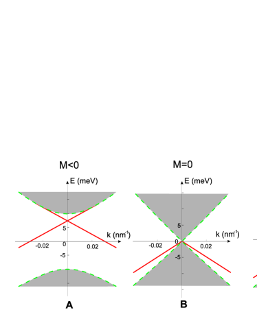
Here, we have , , , , and is the width of the strip. This solution naturally contains both helical edge states () and bulk states (), which are shown in Fig. 1 for three cases , , and . The edge states (red lines in Fig. 1) are seen beyond the bulk gap for all cases, up to an dependent maximum energy. When , the edge states cross the bulk gap producing a topological insulator. At the edge states exist only in conjunction with the lower band, terminating at the Dirac point. For positive there are no edge states in the gap, producing a conventional insulator.Bernevig06SCI
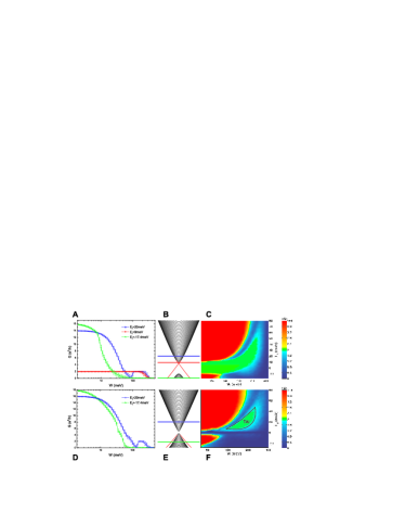
We next study transport as a function of disorder, with the Fermi energy varying through all regions of the band structure. For this purpose, we use a tight-binding lattice model which produces the above Hamiltonian as its continuum limitBernevig06SCI , and following a common practice in the study of Anderson localization, introduce disorder through random on-site energy with a uniform distribution within . We calculate the conductance of disordered strips of width and length using the Landauer-Büttiker formalism.Landauer ; Buttiker The conductance as a function of disorder strength is plotted in Fig. 2 for several values of Fermi energy belonging to different band regions for and . The topological nature of the system is revealed by the quantization of conductance at . The following observations can be made.
The calculated behavior conforms to the qualitative expectation for certain situations. For Fermi level in the lower band, for both and , an ordinary Anderson insulator results when the clean limit metal is disordered (green lines in Fig. 2A and 2D). The conductance in this case decays to zero at disorder strength around meV, which is about two times the leading hopping energy meV, and much larger than the clean-limit bulk band gap meV. Here nm is the lattice spacing of the tight-binding model. This energy scale is several times smaller than the critical disorder strength meV for the metal-insulator transition in such a system in 2D, as extracted from one-parameter scaling calculations note1 . The topological insulator (red line in Fig. 2a) is robust, and requires a strong disorder before it eventually yields to a localized state. This is expected as a result of the absence of backscattering in a topological insulator when time-reversal symmetry is preservedKane05PRLb .
The most surprising aspect revealed by our calculations is the appearance of anomalous conductance plateaus at large disorder for situations when the clean limit system is a metal without preexisting edge states. See, for example, the blue lines in Fig. 2A () and Fig. 2D (). The anomalous plateau is formed after the usual metal-insulator transition in such a system. The conductance fluctuations (the error bar in Fig. 2A and 2D) are vanishingly small on the plateaus; at the same time the Fano factor drops to nearly zero indicating the onset of dissipationless transport in this system,Buttiker90 even though the disorder strength in this scenario can be as large as several hundred meV. This state is termed topological Anderson insulator. The quantized conductance cannot be attributed to the relative robustness of edge states against disorder, because it occurs for cases in which no edge states exist in the clean limit! The irrelevance of the clean-limit edge states to this physics is further evidenced from the fact that no anomalous disorder-induced plateaus are seen for the clean limit metal for which bulk and edge states coexist; those exhibit a transition into an ordinary Anderson insulator.
The nature of TAI is further clarified by the phase diagrams shown in Fig. 2C for and in Fig. 2F for . For , the quantized conductance region (green area) of the TAI phase in the upper band is connected continuously with the quantized conductance area of the topological insulator phase of the clean-limit. One cannot distinguish between these two phases by the conductance value. When , however, the anomalous conductance plateau occurs in the highlighted green island labeled TAI, surrounded by an ordinary Anderson insulator. No plateau is seen for energies in the gap, where a trivial insulator is expected. The topology of the TAI phase as well as the absence of preexisting edge states in the clean limit demonstrate that the TAI owes its existence fundamentally to disorder.
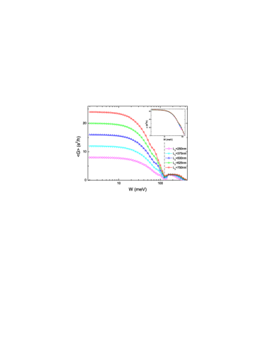
The dissipationless character suggests existence of ballistic edge states in the TAI phase. To gain insight into this issue, we investigate how the conductance scales with the width of the strip. Fig. 3 shows the calculated conductances of a strip as a function of its width . In the region before the TAI phase is reached, the scaled conductance , or conductivity, is width independent, as shown in the inset of Fig. 3, which implies bulk transport. Within the TAI phase, absence of such scaling indicates a total suppression of the bulk conduction, thus confirming presence of conducting edge states in an otherwise localized system.
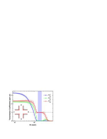
We further examine the picture of edge-state transport in the TAI phase in a four-terminal cross-bar setup by calculating the spin resolved transmission coefficients () between each ordered pair of leads and (). Time-reversal symmetry guarantees that , so it suffices to discuss only one spin component. Three independent coefficients, , and , are shown in Fig. 4 as a function of the disorder strength inside the cross region. The shadowed area marks the TAI phase, where , , and all transmission coefficients exhibit vanishingly small fluctuations. From symmetry, it follows that
| (10) |
and all other coefficients are vanishing small. These facts are easy to understand from the presence of a chiral edge state for the spin up block in the TAI phase. Two consequences of this chiral edge state transport are a vanishing diagonal conductance and a quantized Hall conductance , analogous to Haldane’s model for the integer quantum Hall effect with parity anomaly.Haldane88PRL The quantized Hall conductance reveals that the topologically invariant Chern number of this state is equal to one.Thouless82PRL ; Niu85PRB ; Lee08PRL Since the Hamiltonian for spin down sector is the time reversal counterpart of for the spin up sector, we have the relations The absence of Hall current in a time reversal invariant system implies . Thus, the chiral edge state in the spin down sector moves in the opposite direction as the edge state in the spin up sector. As a result, the total longitudinal conductance and Hall conductance both vanish as in an ordinary insulator, but the dimensionless spin Hall conductance , resulting in quantum spin Hall effect.Kane05PRL
Our work thus predicts quantized conductance in the presence of strong disorder, even when the band structure has positive gap (i.e. no inversion) and the clean limit system is an ordinary metal. We believe that HgTe/CdTe quantum wells, which have been used to investigate topological insulators in the clean limit, are a promising candidate also for an experimental determination of the phase diagram of the topological insulator as a function of disorder and doping, because they enable a control of various parameters through variations in the quantum well thickness and gate voltage.Becker00PRB ; Zhang01PRB The effect of disorder in three dimensional topological insulators should also prove interesting.
The authors would like to thank F. C. Zhang for discussions. This work was supported by the Research Grant Council of Hong Kong under Grant No. HKU 7037/08P.
References
- (1) E. Abrahams, P. W. Anderson, D. C. Licciardello and T. V. Ramakrishnan, Phys. Rev. Lett. 42, 673 (1979).
- (2) S. Hikami, A. I. Larkin, and Y. Nagaoka, Prog. Theor. Phys. 63, 707 (1980).
- (3) T. Ando, Phys. Rev. B 40, 5325 (1989).
- (4) S. V. Kravchenko, G. V. Kravchenko, J. E. Furneaux, V. M. Pudalov, M. D’Iorio, Phys. Rev. B 50, 8039 (1994).
- (5) K. v. Klitzing, G. Dorda and M. Pepper, Phys. Rev. Lett. 45, 494 (1980).
- (6) D. C. Tsui, H. L. Stormer, A. C. Gossard, Phys. Rev. Lett. 48, 1559 (1982).
- (7) S. Das Sarma and A. Pinczuk, Perspectives in Quantum Hall Effects: Novel Quantum Liquids in Low-Dimensional Semiconductor Structures. (Wiley, New York, 1997).
- (8) C. L. Kane and E. J. Mele, Phys. Rev. Lett. 95, 226801 (2005).
- (9) B. A. Bernevig, T. L. Hughes, and S. C. Zhang, Science 314, 1757 (2006).
- (10) C. L. Kane and E. J. Mele, Phys. Rev. Lett. 95, 146802 (2005).
- (11) D. J. Thouless, M. Kohmoto, M. P. Nightingale, and M den Nijs, Phys. Rev. Lett. 49, 405 (1982).
- (12) C. Xu and J. E. Moore, Phys. Rev. B 73, 045322 (2006).
- (13) C. Wu, B. A. Bernevig, and S. C. Zhang, Phys. Rev. Lett. 96, 106401 (2006).
- (14) M. Konig, S. Wiedmann, C. Brune, A. Roth, H. Buhmann, L. W. Molenkamp, X. L. Qi, and S. C. Zhang, Science 318, 766 (2007).
- (15) L. Fu, C. L. Kane, and E. J. Mele, Phys. Rev. Lett. 98, 106803 (2007).
- (16) S. Murakami, New J. Phys. 9, 356 (2007).
- (17) D. Hsieh, D. Qian, L. Wray, Y. Xia, Y. S. Hor, R. J. Cava, and M. Z. Hasan, Nature 452, 970 (2008).
- (18) M. König, H. Buhmann, L. W. Molenkamp, T. L. Hughes, C. X. Liu, X. L. Qi, and S. C. Zhang, J. Phys. Soc. Jpn. 77, 031007 (2008).
- (19) B. Zhou, H. Z. Lu, R. L. Chu, S. Q. Shen, and Q. Niu, to appear in Phys. Rev. Lett. (2008)/arXiv: 0806.4810v1.
- (20) R. Landauer, Phil. Mag. 21, 863 (1970).
- (21) M. Büttiker, Phys. Rev. B 38, 9375 (1988).
- (22) The one-parameter scaling calculations indicate that the metal-insulator transition occurs in the 2D system of this material where electron-electron interaction is absent, and the term in Eq. (1) plays the role of spin-orbit interaction like the Rashba coupling.
- (23) M. Büttiker, Phys. Rev. Lett. 65, 2901 (1990).
- (24) F. D. M. Haldane, Phys. Rev. Lett. 61, 2015 (1988).
- (25) Q. Niu, D. J. Thouless, and Y. S. Wu, Phys. Rev. B 31, 3372 (1985).
- (26) S. S. Lee and S. Ryu, Phys. Rev. Lett. 100, 186807 (2008).
- (27) C. R. Becker, V. Latussek, A. Pfeuffer-Jeschke, G. Landwehr, and L. W. Molenkamp, Phys. Rev. B 62, 10353 (2000).
- (28) X. C. Zhang, A. Pfeuffer-Jeschke, K. Ortner, V. Hock, H. Buhmann, C. R. Becker, and G. Landwehr, Phys. Rev. B 63, 245305 (2001).