Very simple FET amplifier with a voltage noise floor less than 1 nV
Abstract
A field-effect transistor (FET) amplifier for small voltage signals is presented. Its design is elementary and the construction can be afforded by anyone. Despite its simplicity, with a voltage noise less than , it outperforms commercially available integrated FET amplifiers. The amplifier has a gain flatness better than over bandwidth; it can be employed as a front-end for signal analyzers or signal recovery systems.
pacs:
05.40.Ca, 07.50.-e, 07.50.Qx, 84.30.LeKeywords low noise amplifier; FET amplifier; cascode
1 Introduction
The experimentalists often need a preamplifier for small voltage signals with an high input impedance and the lowest possible noise.
Amplifiers based on commercial field-effect transistors (FET) integrated circuits (IC) are very simple to construct, and provide a number of friendly properties (internal compensation, wide bandwidth, wide supply voltage range, high power-supply rejection ratio, etc). However, they have equivalent input voltage noise not lower than nV. On the other end, the construction and trimming of amplifiers based on discrete FETs (see e.g. Refs. [1, 2, 3, 4, 5, 6]) could be sometimes tough for the general experimentalist.
In the following, we describe a very simple FET amplifier, which construction simplicity is comparable to those of IC-based amplifiers. It has a number of friendly properties and its voltage noise floor is better than 1 nV.
2 The circuit
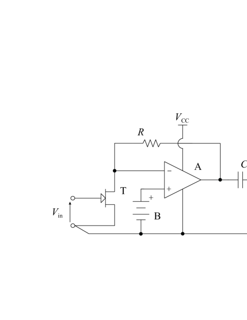
The circuit is shown in Fig. 1.
The transistor T, directly connected to the input voltage , is an FET in an common-source configuration. T works with a gate-source bias voltage . 111A drawback of such configuration is the limited dynamic range, a few tens of at the input, before distortion occurs.
The wiring to proposed in Fig. 1 allows a a pseudo-differential configuration. This can help in reducing interferences or, in correlation measurements [7], permits a four-terminal connection to the device under test.
The op amp A works as a transresistance amplifier with gain , and sets the FET transistor in a cascode configuration [8, 9] (which eliminates the Miller effect [10], thus enhancing the bandwidth). The drain-source voltage is set by A at the voltage of the polarization battery B. B is practically unloaded ( is the small bias current of A), hence it has a long life, and has an extremely low noise [11].
A works in a single-supply configuration; its output is ac-coupled through capacitor , and can be further amplified by additional stages if necessary.
The overall low-frequency gain of the amplifier depends on and the FET transconductance , which can have significant deviations from one sample to another. Therefore, depending on the application, a calibration of with a reference signal may become necessary [7].
Several other properties of the amplfier, like the compensation, bandwidth flatness, large supply voltage range, high power-supply rejection ratio (PSRR), are given by A.
Typical supply voltage is V from an unregulated battery; the power load is .
3 Experimental
The circuit is simple to construct and does not require any trimming.
Examples of suitable low-noise FETs are 2SK170 (Toshiba), LSK170 (Linear Systems), LSK389 (dual FET, Linear Systems); Tab. 1 shows an extract of the corresponding datasheets. A prototype has been assembled with a 2SK170, using an OP27 (various suppliers) for A. We set . The bias current is (measured with a Keithley mod. 6430 current meter), which gives a current shot noise less than .
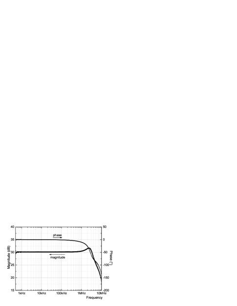
The transfer function of the amplfier is shown in Fig. 2. It has been measured with a network analyzer (Agilent Tech. mod. 4395A), injecting the signal with a resistive divider ( Ω- Ω). A -bandwidth of can be estimated, with a gain flatness better than up to 1 MHz.
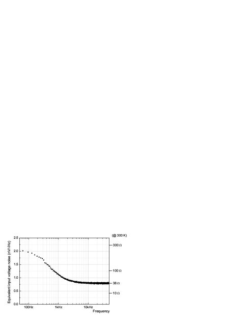
The equivalent input voltage noise with short-circuited input is shown in Fig. 3. It has been measured with a two-channel signal analyzer (Agilent Tech. mod. 35670A) by connecting to both channels and performing a cross-correlation measurement in order to reject the analyzer noise. The noise floor is , corresponding to the Johnson noise of a Ω resistor at .
4 Conclusions
The amplifier can be of interest in a number of applications, in particular as an input front-end for commercial instrumentation (signal analyzers, lock-in amplifiers).
Two protypes of the amplifier have been employed in a correlation spectrum analyzer, developed for accurate measurement of the Johnson noise of a resistor [7]. The experiment is still under development, but the amplifier has shown excellent properties, comparable with more sophisticated setups [6]. Despite the open-loop configuration, after an initial warm-up time the gain mid-term stability is within one part in in a laboratory environment.
Acknowledgments
The authors warmly thank Massimo Ortolano, Politecnico di Torino, for fruitful discussions and for reviewing the manuscript.
References
- [1] H. H. Klein, G. Klempt, and L. Storm. Measurement of the thermodynamic temperature of 4He at various vapour pressures by a noise thermometer. Metrologia, 15:143–154, 1979.
- [2] S. R. Jefferts. A very low-noise fet input amplifier. Rev. Sci. Instrum., 60:1194–1196, Jun 1989.
- [3] B. Neri, B. Pellegrini, and R. Saletti. Ultra low-noise preamplifier for low-frequency noise measurements in electron devices. IEEE Trans. Instr. Meas., 40:2–6, Feb 1991.
- [4] R.M. Howard. Low noise amplifier design and low noise amplifiers for characterizing the low frequency noise of infrared detectors. Optoelectronic and Microelectronic Materials Devices, 1998. Proceedings. 1998 Conference on, pages 179–182, 1999. See Fig. 5.
- [5] G. Ferrari and M. Sampietro. Correlation spectrum analyzer for direct measurement of device current noise. Rev. Sci. Instrum., 73:2717–2723, July 2002.
- [6] J. T. Zhang and S. Xue. A noise thermometry investigation of the melting point of gallium at the NIM. Metrologia, 43:273–277, 2006.
- [7] M. Pisani L. Callegaro and A. Pollarolo. Traceable Johnson noise measurements in the audio frequency range. In CPEM 2008 Conf. Digest, Broomfield, CO, USA, Jun 2008. in press.
- [8] F. V. Hunt and R. W. Hickman. On electronic voltage stabilizers. Rev. Sci. Instrum., 10:6–21, January 1939.
- [9] P. Horowitz and W. Hill. The art of electronics. Cambridge University Press, 2nd edition edition, 1989.
- [10] J. M. Miller. Dependence of the input impedance of a three-electrode vacuum tube upon the load in the plate circuit. Scient. Papers Bureau of Standards, 15:367–385, 1919-20.
- [11] C. K. Boggs, A. D. Doak, and F. L. Walls. Measurement of voltage noise in chemical batteries. Frequency Control Symposium, 1995. 49th., Proceedings of the 1995 IEEE International, pages 367–373, May-2 Jun 1995.
| Symbol | description | 2SK170BL | LSK170B | LSK389B |
|---|---|---|---|---|
| transconductance | ||||
| noise voltage ( ) | ||||
| input capacitance | ||||
| drain current |