Slow conductance relaxations; Distinguishing the Electron Glass from extrinsic mechanisms
Abstract
Slow conductance relaxations are observable in a many condensed matter systems. These are sometimes described as manifestations of a glassy phase. The underlying mechanisms responsible for the slow dynamics are often due to structural changes which modify the potential landscape experienced by the charge-carriers and thus are reflected in the conductance. Sluggish conductance dynamics may however originate from the interplay between electron-electron interactions and quenched disorder. Examples for both scenarios and the experimental features that should help to distinguish between them are shown and discussed. In particular, it is suggested that the ‘memory-dip’ observable through field-effect measurements is a characteristic signature of the inherent electron-glass provided it obeys certain conditions.
pacs:
72.80.Ng 73.61.Jc 72.20.EeI Introduction
Many phenomena in solid state systems involve slow conductance changes. The phenomenon that has been most studied in this context is conductance noise, which often exhibits a 1/f power-spectrum. In degenerate Fermi systems (metals, heavily-doped semiconductors) the prevalent view is that the fluctuations in the conductance reflect temporal changes in the potential experienced by the charge carriers 1 . Such potential fluctuations may be structural, involving slow dynamics of ions/atoms which, in turn, may be triggered by a modified state of local charge following, for example, electronic re-arrangement of valence electrons. These as well as ”purely” ionic displacement are referred to in this paper as structural two-level-systems. Slow release/trapping of carriers will likewise manifest itself in slow conductance fluctuations. Either mechanism may lead to conductance fluctuations that typically extend to very low frequencies 1 .
As a rule, 1/f experiments were performed in systems where the average was time independent, namely, in equilibrium or near equilibrium situations. There are however many cases where itself changes slowly with time, which, by definition suggests a non-equilibrium phenomenon. This may occur for example due to annealing of defects, neutron irradiation, diffusion of an injected dopant, illumination by light, and many other instances involving changes of the potential landscape, or the density of carriers in the conducting system. It often happens in these cases that the sluggish response observed in exhibits features that are characteristic of glasses. Experimental results illustrating two mechanisms for such ‘extrinsic’ glassy effects in conductivity will be shown and discussed in section III.
Glassy effects in may arise from an intrinsic mechanism, in which case both the ions potential and the carriers density may be, in theory, time independent. Glassy behavior of the electronic system in a system with quenched disorder has been anticipated by several authors 2 ; 3 ; 4 ; 5 . This new type of a non-ergodic system was first termed Electron Glass by Davies et al referring to a system with localized electronic states interacting via an un-screened Coulomb interaction 4 . Glassy effects inherent to the electronic systems that may arise even in the non-interacting system were also considered 3 . However, common to all models of intrinsic electron glass is a sufficiently strong static disorder such that the electronic states are Anderson localized. This is one of the essential differences between the electron glass and the extrinsic mechanisms alluded to above. In the latter, glassy effects may manifest themselves even when the transport mode is diffusive. By contrast, a pre-requisite for intrinsic electron glass behavior is that the system is Anderson localized, and thus charge transport must be activated. This condition is necessary but not sufficient, more detailed criteria will be given in the discussion section below.
Non-ergodic effects such as slow relaxation, aging, and other memory effects associated with electron glass behavior were reported in few systems 6 ; 7 ; 8 ; 9 ; 10 ; 11 . Naturally, the question of extrinsic effects dominating, or at least, contributing to the measured effects have been considered in early publications 12 .
There are difficulties in categorically ruling out extrinsic effects; Essentially all glasses, whether mechanical, magnetic, or electronic, show similar dynamical features. While these universal attributes give the impetus to study glasses, the similar effects make it hard to distinguish between different glasses, especially when both types are revealed through the same measurable (i.e., conductance). Current theories of the electron glass are not sufficiently detailed to allow this differentiation. The one issue on which theory predicts a qualitative feature that, experimentally, seems to be peculiar to the electron glass, is the law of relaxation being logarithmic in time 13 . This has indeed been verified in several electron glasses 8 , and in this relaxation law has been observed over almost 6 decades in time 14 . It was also shown in this system that the ions/atoms dynamics is associated with quite different time scales and spatial scales than the dynamics of the electron glass 15 . Similar results were obtained on granular al films by Grenet and by Delahaye et al 16 . However, the most compelling evidence for an inherent electron glass is the dramatic dependence of the glassy properties on the system carrier concentration 17 . This will be further elucidated in this paper.
In some cases it is possible to identify the origin of the glassy effects in as arising from an extrinsic mechanism. Two examples that are probably characteristics of a wide range of phenomena will be described in section III. We then describe for comparison the salient features of the electron glass and discuss the differences.
A modest conclusion that one may draw is that there are two types of glassy electronic systems; those that can be unambiguously shown to be extrinsic, and those that cannot, and for which the only consistent scenario is the electron glass. However, we will argue that, on empirical basis, there is a positive test for the electron glass; This is the memory dip that on one hand is unequivocally associated with all the glassy features of the system, and on the other hand its characteristic width is determined by the carrier concentration of the material. The special features of the memory dip that are suggestive of an electronic mechanism will be detailed and discussed.
II Experimental
II.1 Sample preparation and measurement techniques
Several batches of samples were used in this study. These were thin films of either polycrystalline or amorphous indium-oxide (to be referred to as and respectively). The films were deposited by an e-gun using 99.999% pure . The amorphous films are typically 80-200 Å thick, while the polycrystalline films have typically a thickness of 30-60 Å. As deposited indium-oxide films onto room temperature substrates are amorphous. Polycrystalline films were prepared by heating the sample to K after deposition. The sheet resistance of either structure was adjusted by thermal annealing (for ) or UV-treatment (for ), to be within the range 2 M-100 Mat 4K for the electron glass studies. All samples had lateral dimensions of 1x1 mm. Some samples were configured as a field-effect devices using either: 110m cover glass as spacers and a gold film evaporated on the backside as gate, or 0.5m thermally grown SiO2 spacer on heavily doped Si wafer as gate. The 110m spacer is used unless otherwise specifically mentioned. This is so as to enable the use of reasonably high frequency in the conductance measurements even for samples with very high resistance (note that the sample/gate capacitance is in parallel with the ac measurement 6 , and the RC problem limits the to low value thus compromising the temporal resolution and the signal/noise value). The 0.5m spacer is used when it is desirable to cover a wide range of charge variation in the field effect measurements without using an excessively large voltage. Conductivity of the samples was measured using a two terminal ac technique employing a 1211-ITHACO current preamplifier and a PAR-124A lock-in amplifier for the 4K studies, and straightforward resistance measurements using HP34401A for the room temperature measurements. Fuller details of sample preparation, characterization, and measurements techniques are given elsewhere 6 ; 11 ; 18 . All resistance data reported here are per square geometry (namely, data are specified in terms of the appropriate two dimensional resistivity).
III Results and discussion
Glassy features are readily observed in conductivity, and they may be associated with various mechanisms. In this section we show and discuss some experimental results of two groups of glassy effects revealed in conductance measurements. Examples of glassy effects observable in the conductance that can be shown to be due to extrinsic mechanisms are given in the next subsection. This is followed by a list of features that should help to distinguish the intrinsic electron glass from the extrinsic glass. In both cases, the data used for illustration were deliberately taken on the same systems namely, and . The different glassy mechanisms were achieved by varying the sample parameters (disorder) and the external conditions used in the measurements (in particular, temperature).
III.1 Glassy effects due to extrinsic mechanisms
The first example we discuss in this category is the process of thermal annealing, commonly used to reduce the resistance of amorphous indium-oxide films, 18 ; 19 . This involves holding the samples at a constant temperature, typically up to few tens of degrees above room temperature, and monitor the resistance versus time as shown in Fig. 1 for a series of samples, all made at the same deposition run. Note that depicted here on a semi-log scale, exhibits non-exponential relaxation. The observed slow decrease in is an irreversible process and is due to elimination of micro-voids which are common in amorphous materials prepared by quench cooling 20 . Naturally, this process also affects the density of the material, namely, the sample volume shrinks as was directly confirmed by optical measurements 21 . This leads to a better wave-function overlap and thus enhances the conductance. The slow relaxation of is then just a reflection of the slow dynamics involved in the compaction process of the material. The initial resistances of the samples used in Fig. 1 were of the order of 1-2 M, rather deep into the insulating regime making their conductance very sensitive to even small changes of the landscape potential, and this is the only reason for choosing them for the illustration. In fact, slow conductance relaxations were observed even in samples that are well-annealed to be on the metallic side of the transition 21 .
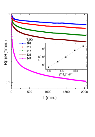
Note that at any given time during the process increases rather fast with annealing temperature , which varies by only % in the series. This presumably means that the annealing process is activated, consistent with thermally assisted atoms diffusion. A way to characterize the dynamics is to monitor the time it takes for to decay to a given fraction from its initial value. (This is, admittedly, an arbitrary definition for a relaxation law that does not have a characteristic scale but any other sensible definition will not change our conclusions). In the inset to Fig. 1 we plot the dependence of on temperature. As it turns out follows a temperature dependence of the Vogel-Fultcher-Tammann type 22 ; , a typical behavior for many classical glasses. The apparent divergence of at K (see inset to Fig. 1) has a simple and plausible interpretation: The samples were prepared and handled at or close to room temperatures prior to being subjected to the annealing process, and thus they were already well annealed at . No glassy dynamics of this kind is observed with such samples at or below liquid nitrogen temperatures.

Another set of glassy behavior observable through conductance measurement is illustrated in Fig. 2. Here we utilize the flexibility of fine-tuning the resistance of films by UV-treatment. Unlike the thermal annealing, this process is reversible, which is useful for many studies. While under pumping, and constant UV illumination, the film resistance decreases slowly. Breaking the vacuum by bleeding oxygen into the system reverses the trend. Fig. 2 includes several cycles of UV-exposure+pumping, alternating with bleeding-air periods resulting in a time sequence of that obviously retains some ”memory” of previous conditions. A fit to a stretched exponential can be easily obtained for each of the relaxations in Fig. 2. In fact, as shown for example in the inset, for one of the ‘recovery’ processes (which is cheap to maintain for a long time), one could obtain an impressive fit to a stretched exponential dependence extending over several weeks (more than 5 decades in time!)
History-dependence and stretched exponential behavior are sometimes taken as a test of a ”glass”, so this example might have been considered a bona-fide indication of ”electronic” glass. Note though that the sample here is actually diffusive, and therefore it can not be an electron glass, at least not from the point of view of the theories 2 ; 3 ; 4 ; 5 . Actually, the reason for these slow conductance changes turns out to be associated with change of stoichiometry in the system. A plausible scenario that accounts for the glass-like dynamics in this case may be understood by studying the structural changes caused by the UV-treatment process.
Indium-oxide films, whether amorphous or crystalline, are oxygen deficient version of the ionic compound and this non-stoichiometry gives rise to ‘free’ carriers (electron) density . The further is in for example, the larger is All other things being equal, larger yields higher conductivity. This is essentially the same process as when a semiconductor is doped by n-type impurities, except that the smallest feasible in stable films (cm is already sufficient to make the system a degenerate Fermi gas. More importantly, the process of ”doping” here is easily affected by UV illumination, which breaks the oxygen bonds, then pumping away the oxygen atoms increases of the host. Exposing the sample to oxygen-rich atmosphere reverses the process. Naturally, the processes of ”doping” and ”un-doping” are reflected in the conductivity. The change of with the UV-treatment (and the consequential mobility modification) were studied by a variety of ways including Hall effect, and Burstein shifts using optical absorption 23 . Similar effects are observable in other materials such as and they are sometimes referred to as ‘persistent photo-conductivity’ 24 a term originally reserved for electron-hole creation in semiconductors rather than reflecting a change of the system chemistry 25 . Another case of an extrinsic effect that manifests itself as slow conductance relaxation is the infamous ”DX center” phenomenon. This is now believed to be a structural effect well studied in semiconductors 26 .
The reason for the sluggish response of the conductance are barriers that the oxygen atoms have to overcome in crossing the film surface, and barriers for the atoms to diffuse into the bulk of the film. The dynamics of these processes in general depends on a number of factors such as the crystallite size, thickness of the film, and disorder (which makes the relevant barriers a function of space, and thus distribute the diffusion rates over a wide range. The phenomenon is also extremely sensitive to temperature; For example, the hump in the curve between 12 to 16 days (inset to Fig. 2) resulted from the temperature in the room increasing by K (less than 1% change!)
Extrinsic glasses are interesting by their own right; the ease of monitoring the underlying dynamics via the flexible conductance measurement has many advantages for the study of the underlying glassy effects. The conductance in these cases may then reflect all the basic glass features including aging and other memory effects. However, such extrinsic glasses must not be confused with the electron glass. There are some obvious differences between the electron-glass and the extrinsic ‘conductivity-glasses’ described above (and many others of similar nature) such as temperature and its effect on dynamics, and law of relaxation. It is desirable however to have a qualitative test that distinguishes the inherent electron glass from extrinsic mechanisms. Such a test is the existence of a memory dip, a feature that is probed by a field effect measurement. It has phenomenology which is peculiar to the electron glass, as will be detailed in sub-section c below.
III.2 Intrinsic electron-glassy effects
In theory, glassy effects in the conductance may originate from the interplay between disorder and interactions while the ions are stationary. In fact, sufficiently strong spatial disorder, such that the electronic states are localized, is claimed to lead to a glassy state even in the non-interacting system 3 (Fermi glass). The presence of disorder however, has other consequences; in the first place it gives rise to two-level-systems that, in turn, manifest themselves in a wide spectrum of 1/f noise extending to very low frequencies 1 . This means that, even near equilibrium, ion/atom dynamics occurs on time scales that, partially, overlaps with typical relaxation times of the electron glass, as already remarked elsewhere 12 . Measurements on mesoscopic samples of showed that the electron glass dynamics occurs on a much shorter time scale (and different spatial scale) than the dynamics associated with structural TLS suggesting that the two phenomena are of different origin 15 . It seems plausible that the two phenomena should influence one another, but there is yet no evidence for such an effect. In particular, we failed to detect any specific contribution to the 1/f noise due to the glassy state; for example, no measurable change of noise could be detected when the sample was kept out of equilibrium by a continuous excitation (created by continuously sweeping the gate voltage).
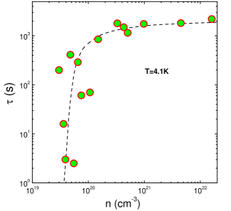
The other issue that the localization brings about is the impaired screening, which makes the notion of a Fermi glass (non-interacting) of somewhat academic scenario. Indeed, electron-electron interactions are believed to essential for the existence of the glassy phase 4 ; 5 . Experimentally, the relevance of interactions in real systems is evidenced by the observation that, all other things being equal, the typical relaxation time of the electron glass is controlled by the carrier concentration of the system 17 . Using a series of films of similar resistance it was shown that varies by 3 orders of magnitude for a change of a mere factor 4 in This is illustrated in Fig. 3 (based on data from 17 and newer data added recently using similar techniques). Other sample parameters such as resistance, magnetic field, and temperature have a much smaller effect on 12 ; 27 ; 28 . Finally, has been essentially unchanged when the sample spatial extent has been varied from 1 cm down to 2 15 , and is also independent of thickness within the range studied. Vaknin et al 17 argued that these results imply the importance of electron-electron interactions. It should be noted that the change in in this series of samples amounts to changing the In/O ratio in the preparation stage by a few percent. This hardly influences any structural aspects and therefore it is hard to reconcile this observation with any ‘extrinsic’ mechanism. It should also be emphasized that these results are in agreement with other methods of measuring the dynamics. These methods were fully described in 27 ; 28 . The physics of this dramatic dependence on n shown in Fig. 3, which empirically accounts for the absence of inherent slow relaxation in low density systems (e.g., lightly-doped semiconductors as will be further discussed below), has been interpreted as a quantum friction effect in 28 .
The other systems that show electron glassy effects (i.e., and granular metals) lack the flexibility of varying over a substantial range. (may be easily varied in semiconductors but their appears to be quite short due to reasons explained elsewhere 17 ; 28 ). There is however, one feature that is common to all (inherent) electron glasses - this is the memory dip (MD). The MD appears in field effect measurements as a minimum of the conductance versus gate voltage centered around the gate voltage where the system was allowed to equilibrate 9 ; 11 ; 12 . It was initially termed ‘anomalous field effect’ by Ben-Chorin et al where it was realized only in ‘note-added-in-proof’ that it is a non-equilibrium effect 6 . As more elaborate experiments became available, the intimate connection between this ‘anomaly’ and the electron glass properties became evident. In fact, every single aspect of the electron glass, such as slow relaxation, memory effects, and aging is reflected in the temporal behavior of the MD 11 . For example, it was shown that history dependence, such as aging, is wiped-out when the MD is destroyed by either exposure to infrared source or non-ohmic field 29 . Also, for a given system, the electron glass dynamics, as well as its temperature dependence, is uniquely characterized by the MD width 28 .
III.3 The memory dip (MD) properties
The physics underlying the function we refer to as MD is not yet well understood. Several authors have conjectured that the MD is a reflection of the Coulomb gap 30 ; 31 ; 32 ; 33 . Adopting this view indeed helps to understand some of the non-trivial features exhibited by of electron-glasses, such as the two-dip experiment 10 ; 12 . On the other hand, some difficulties with this interpretation were also pointed out 9 ; 17 . In the following, these reservations will be re-examined in view of recent experiments.
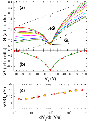
We start by reviewing the basic properties of the phenomenon at a given temperature, as the great majority of experiments were performed at or around 4K. The MD revealed in the scans is characterized by its relative amplitude and by its shape (functional form). There are several variables that may affect appreciably however, the functional form of the MD is independent of any of these variables. For example, increasing the sweep rate of the gate voltage increases (logarithmically, see, Fig. 4a,c) yet, upon re-scaling just the y-axis, the MD of two scans with quite different would perfectly overlap one another (Fig. 4b). The dependence on sweep-rate (that in this work has been extended to cover more than 3 decades) also illustrates that the MD is a non-equilibrium phenomenon as well as the basic dynamics.
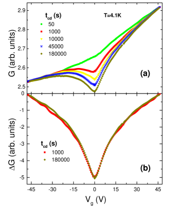
Another factor that affects the amplitude but not the shape of the MD is the time during which the system equilibrates after the initial cool-down to the measurement temperature (Fig. 5). The evolution of with time at =0 is just the law of the electron glass that one observes in , say after a quench from high temperature (even without configuring the sample with a gate). The interesting thing here is that while this conductance ‘equilibration point’ is slowly going down it ”drags” with it some region around =0 in such a manner to keep the shape of the symmetric field effect (i.e., the MD) constant (c.f., inset to Fig. 5). Note that this region extends over a rather large range of a point to which we shall return below.
Finally, two other factors that do not affect the MD shape; Disorder and magnetic field. By higher disorder we refer to samples that are deeper into the insulating phase. This is manifested by a larger at a given Both, the slope of asymmetric field effect and of the MD increase with the sample resistance. However, disorder has no effect on the shape of the MD 11 . A magnetic field as high as 30T, while changing by as much as a factor 34 of 4, which naturally also affects the equilibrium (asymmetric) part of the field effect, does not change the MD shape (Fig. 6). Interestingly, the magnetic field changes both and in such a way that is constant. Other agents that modify , also change The reason for that is not currently understood.
The only factor that, at a fixed temperature, does affect the MD shape is the carrier concentration of the system. The characteristic width of the MD (to be defined below) increases monotonically with and that seems to be a ‘universal’ feature, common to all electron glasses studied to date and granular metals 15 . Note that this observation clearly implicates an electronic mechanism, and qualitatively it is in line with the Efros-Shklovskii Coulomb gap 35 ; 36 , which increases monotonically with the density of states 36 . As mentioned in section I, the possibility that a Coulomb gap (or, more generally, an interaction gap) is the underlying physics of the MD was considered, but several reservations were raised against it. A serious concern is the relevance of a single-particle density-of-states (DOS) to conductance. In addition, a severe problem was a factor of discrepancy 17 between the experimental results for the width of the MD and the value expected for the strength of the Coulomb interaction (17 used , with a dielectric constant and as a measure of this energy).
It is this discrepancy that we wish to re-examine here and show that it was based on a definition of width that, though natural, may have underestimated its value.

The definition of the MD width adopted by Vaknin et al 17 is based on measuring the width (in volts) of the MD at half-height from the scan. Using the gate-sample capacitance the width in terms of the associated charge is obtained Note that it is this charge range rather than the voltage span which is the relevant variable to characterize the width of the MD. This has been demonstrated by comparing FET samples with different spacers and spacer thickness for a given electron glass 11 . Then, the width in energy units is derived with the associated with the half-height and the calculated density of states using the measured and free electron formulae.
Since the half-height of the MD (to be referred to as is experimentally well-defined, this procedure of assigning a width to a particular sample is convenient and unambiguous. However, if the modulation in or more precisely, , reflects a DOS versus energy structure, then the shape of the MD would depend on temperature due to the thermal occupation of states. This indeed seems to be the case; the MD gets broader as increases 37 . The price for the experimentally convenient definition is a spurious temperature dependent energy scale. In simple words, the temperature dependence of is an artifact that arises from the non-linear mapping between added charge, and the associated energy change. This point was elaborated on by Lebanon and Mueller that, using a model, showed that the MD shape becomes more ”cusp-like” as the temperature is reduced is a way that qualitatively resembles the experiments 33 (however, the specific relation between the assumed DOS and is still to be justified). Using the ‘half-height’ criterion for comparison with the Coulomb gap width is therefore problematic, which, in hindsight, being temperature dependent was was not relevant for the comparison to start with.
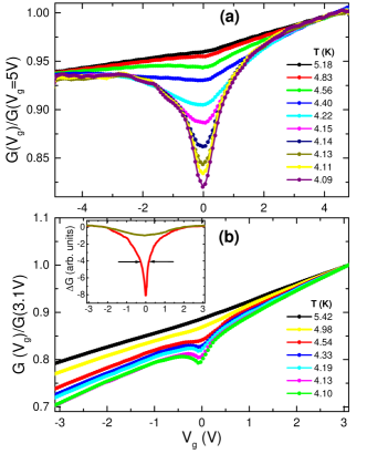
An alternative way to define the energy scale associated with the MD suggests itself when one studies the temporal evolution of after a quench-cool from high temperature as shown in Fig. 5 above. Note that the scans of this sample show time dependence throughout the interval (-50 V to +50 V) while outside it tend to approach a time independent regime. The precise boundaries of this region may be ill defined, yet obviously, the ‘active’ energy band extends over a wide range that does not depend on time or on . It makes sense then to use this ‘active’ region as the relevant scale and derive the MD width (henceforth labelled from it. Indeed, this definition for the MD width turns out also to be temperature independent. This is illustrated in Fig. 7a for a sample, and in Fig. 7b for . (Note that in these experiments, the equilibrium (asymmetric) part of the field effect changes with temperature. This results from the the higher sensitivity of as the temperature is lowered and increases (compare with Fig. 5 where is fixed). Note incidentally that the slope of the equilibrium field effect in is considerably smaller than that of the sample (Fig. 7). This is a result of the shallower slope of the thermodynamic DOS versus energy in the amorphous material.
The pronounced temperature dependence of of these samples are shown in Fig. 8a. For comparison, the dependence of the half-height width on temperature for a FET sample with a much thicker spacer is shown in Fig. 8b, which shows that at a given does scale with the thickness of the spacer (which affects the sample-gate capacitance) as mentioned above.
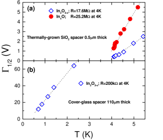
The ratio where is taken at 4K), is for the in Fig. 7a, and for the sample in Fig. 7b, and a ratio of 7-10 was found for the series of samples with in the range 6 cm-3 to 8 cm-3. In terms of energy, this range amounts to 10-80 meV respectively, a range that compares favorably with the associated electronic energy These values for the MD width are not too far from the values expected for the Efros-Shklovskii Coulomb gap, leads us to re-consider the possible connection between the two.
The main difficulty in trying to compare the MD with the Coulomb gap is related to the different prescriptions for measuring them. The Coulomb gap is a single-particle DOS which, by definition, is associated with adding charge to the system while all other particles are frozen (like, e.g., in tunneling or photo-emission experiment). It is also an equilibrium entity. This is not the situation in the field effect measurements where, for any feasible sweep rate, some relaxation takes place, and when carried out under equilibrium conditions no MD is observed (c.f. the dotted line in Fig. 4a). Nevertheless the two phenomena seem to be linked to a similar energy scale. Clarifying the possible relation between the Coulomb gap and the MD is a challenge to theory.
A related issue is how the ‘interaction-band’ associated with the MD affects the equilibrium conductance Experimentally, the conductance versus temperature in all electron glasses is always activated, as it must be for a system with localized states. However, no characteristic law can be identified. For example, films usually exhibit with when deeply insulating (namely, Mott-like behavior in a 2D system) and when closer to the diffusive regime. Granular metals and films often show stretched exponential with while in granular Al films has been reported 8 . It appears that there is more diversity in the laws of the electron glasses than in their non-equilibrium properties, which are remarkably similar. Therefore, slow conductance relaxation due to the electron glass scenario may be positively identified by the behavior of the associated MD but not by .
III.4 Discussion
The experimental observations detailed above raise the question: What about those systems that do show hopping conductivity yet do not show MD in field effect measurements; are they not electron glasses? This is quite a pertinent question; there are many such systems, notably semiconductors. To our best knowledge, a memory dip has not been reported in any semiconductor even at temperatures lower than 1 K.
Theoretically, the electron glass is generic to a degenerate Fermi system with localized states and Coulomb interactions. The theory conjectures that all such systems are electron glasses (and, by our proposed test, should exhibit MD in field effect measurements). Theory however does not specify the typical relaxation time of a given system, so here again we have to rely on experiment. All experiments performed to date suggest that the relaxation time , and thus the time for the MD to ‘form’ and ‘decay’, is a monotonous function of and relaxation times that are appreciably larger than few seconds are found only in systems with cm
As is shown in Fig. 3, below a certain carrier concentration , drops down extremely fast. Such a ‘critical’ concentration may vary to some degree between different systems, yet it is hard to see what else except (and to a considerably lesser degree ) may have an appreciable effect on for a generic effect that hinges on just localized states and Coulomb interactions 38 . A possible reason for the dramatic dependence based on quantum friction scenario was offered in 28 but here we shall treat this finding on purely empirical grounds. Since semiconductors that are in the hopping regime have typically cm-3 it is quite conceivable that their typical will be much smaller than 1 second, as suggested by Fig. 3. That will make it very hard to see the MD in a field effect experiment, which is an inherently slow process due to the gate-sample capacitance and sample resistance. Simply stated, a consistent answer is that all hopping systems are in principle electron glasses provided their resistance is large enough, and they are measured at low enough temperature. However, if no MD is observed it might mean that their ‘slow’ relaxation is too short to be observed in the field effect. In this situation, observing conductance relaxation for larger time than that which would allow MD detection should be a warning sign of an extrinsic mechanism.
In summary, we discussed the differences between extrinsic and intrinsic glassy effects observed in conductance measurements. A simple test for an intrinsic electron glass has been proposed based on a field effect measurement performed on the system after allowing it to equilibrate. The appearance of a dip with dynamics that precisely coincides with the relaxation of the excess conductance caused by, e.g., a quench from high temperatures, is a primary signature of the electron glass. In addition, the dip should have a characteristic shape that does not depend on disorder, magnetic field, or gate-voltage sweep-rates, and width that is of order of a relevant electronic energy. Moreover, the shape of the dip should depend on temperature even for ; an attribute that is peculiar to the electron glass, quite distinct from thermal smearing.
It would be of great interest to extend the study of the electron glass to include more materials, and in particular, to further test the empirical connection between carrier concentration and relaxation time. Systems that are may be promising in this regard include high-Tc compounds, and transition metal semiconductor alloys, provided that they are sufficiently deep into the hopping regime. On the theoretical side, there is the challenge of dealing with the non-equilibrium DOS that is associated with the memory dip, which seems to be the essence of the electron glass physics.
The author acknowledges with gratitude the hospitality and use of facilities at the NHMFL at Tallahassee, and illuminating discussions with A. L. Efros. This research was supported by a grant administered by the US Israel Binational Science Foundation and by the Israeli Foundation for Sciences and Humanities.
References
- (1) P. Dutta, and P. M. Horn, Rev. Mod. Phys. 53, 497 (1981); M. B. Weissman, Rev. Mod. Phys., 60, 537 (1988), and references therein.
- (2) M. Grünewald, B. Pohlman, L. Schweitzer, and D. Würtz, J. Phys. C, 15, L1153 (1982).
- (3) M. Pollak and M. Ortuño, Sol. Energy Mater., 8, 81 (1982); M. Pollak, Phil. Mag. B 50, 265 (1984).
- (4) J. H. Davies, P. A. Lee, and T. M. Rice, Phys. Rev. Lett., 49, 758 (1982).
- (5) G. Vignale, Phys. Rev. B 36, 8192 (1987).
- (6) M. Ben-Chorin, D. Kowal and Z. Ovadyahu, Phys. Rev. B 44, 3420 (1991).
- (7) G. Martinez-Arizala, D. E. Grupp, C. Christiansen, A. Mack, N. Markovic, Y. Seguchi, and A. M. Goldman, Phys. Rev. Lett., 78, 1130 (1997). G. Martinez-Arizala, C. Christiansen, D. E. Grupp, N. Markovic, A. Mack, and A. M. Goldman, Phys. Rev. B 57, R670 (1998).
- (8) T. Grenet, Eur. Phys. J, 32, 275 (2003); T. Grenet, J. Delahaye, M. Sabra, and F. Gay, Eur. Phys. J. B 56, 183 (2007).
- (9) M. Ben Chorin, Z. Ovadyahu and M. Pollak, Phys. Rev. B 48, 15025 (1993).
- (10) A. Vaknin, Z. Ovadyhau, and M. Pollak, Phys. Rev. Lett., 84, 3402 (2000).
- (11) A. Vaknin, Z. Ovadyahu, and M. Pollak, Phys. Rev. B 65, 134208 (2002).
- (12) M. Ben Chorin, Z. Ovadyahu and M. Pollak, Phys. Rev. B 48, 15025 (1993); Z. Ovadyahu and M. Pollak, Phys. Rev. Lett., 79, 459 (1997).
- (13) Ariel Amir, Yuval Oreg, and Yoseph Imry, Phys. Rev. B 77, 165207 (2008); A. Vaknin, Z. Ovadyahu, and M. Pollak, Phys. Rev. B 61, 6692 (2000).
- (14) Z. Ovadyahu, and M. Pollak, Phys. Rev. B 68, 184204 (2003).
- (15) V. Orlyanchik, and Z. Ovadyahu, Phys. Rev. B 75, 174205 (2007).
- (16) T. Grenet, Phys. Stat. Sol. C 1, 9 (2004); J. Delahaye, T. Grenet and F. Gay, Eur. Phys. J. B 65, 5 (2008).
- (17) A. Vaknin, Z. Ovadyhau, and M. Pollak, Phys. Rev. Lett., 81, 669 (1998).
- (18) Z. Ovadyahu, J. Phys. C: Solid State Phys., 19, 5187 (1986).
- (19) A. T. Fiory, and A. F. Hebard, Phys. Rev. Lett. 52, 2057 (1984); G. Sambandamurthy, L.W. Engel, A. Johansson, and D. Shahar, Phys. Rev. Lett., 92, 107005 (2004).
- (20) N. F. Mott and E. A. Davis, in: ”Electronic Processes in Non-Crystalline Materials”, pp 336-338, Clarendon Press, Oxford (1979).
- (21) Z. Ovadyahu, Phys. Rev B 47, 6161 (1993).
- (22) Jeppe C. Dyre, Rev. Mod. Phys. 78, 953 (2006) and references therein.
- (23) O. Cohen and Z. Ovadyahu, Phys. Rev. B 50, 10442 (1994).
- (24) Z. Y. Xiao, Y. C. Liu, R. Mu, D. X. Zhao, and J. Y. Zhang, Appl. Phys. Lett. 92, 052106 (2008).
- (25) I. Giaever and H. R. Zeller, Journal of Vacuum Science and Technology, 6, 502 (1969); P. Stradins and H. Fritzsche, Phil. Mag. B 69, 121 (1994).
- (26) See e.g., Jingbo Li, Su-Huai Wei, and Lin-Wang Wang, Phys. Rev. Lett., 94, 185501 (2005); S. Lany , H.Wolf , and T. Wichert, Phys. Rev. Lett., 92, 225504 (2004).
- (27) Z. Ovadyahu, Phys. Rev. B 73, 214208 (2006).
- (28) Z. Ovadyahu, Phys. Rev. Lett., 99, 226603 (2007).
- (29) V. Orlyanchik, A.Vaknin, Z. Ovadyahu, and M. Pollak, Phys. Stat. Sol., b230, 61 (2002); V. Orlyanchik and Z. Ovadyahu, Phys. Rev. Lett., 92, 066801 (2004).
- (30) C. C. Yu, Phys. Rev. Lett., 82, 4074 (1999); Physica Status Solidi b230, 47 (2002).
- (31) D. R. Grempel, Europhys. Lett., 66, 854 (2004); A. B. Kolton, D. R. Grempel, and D. Dominguez, Phys. Rev. B 71, 024206 (2005).
- (32) M. Müller and L. B. Ioffe, Phys. Rev. Lett. 93, 256403 (2004).
- (33) Eran Lebanon, and Markus Mueller, Phys. Rev. B 72, 174202 (2005).
- (34) The positive magnetoresistance results from the spin alignment mechanism proposed by: A. Kurobe and H. Kamimura, J. Phys. Soc. Japan, 51, 1904 (1982).
- (35) M. Pollak, Discuss. Faraday Soc. 50, 13 (1970).
- (36) A. L. Efros and B. I. Shklovskii, J. Phys. C: Solid State Phys., 8, L49 (1975).
- (37) A. Vaknin Z. Ovadyahu, and M. Pollak, Europhys. Letters 42, 307 (1998).
- (38) This however is based on experiments in the liquid helium temperature range where is only weakly temperature dependent. It remains to be seen whether long relaxation times are achievable even in systems with low carrier concentration when cooled to ultra low temperatures (while still of measurable resistance).