The mechanism of ion induced amorphization in Si
Abstract
Some results on damage build up in, and amorphization of, Si, induced by 25-30 keV Al, Si and Cs- ions, at room temperature, are reported. We show that at low energy, amorphization is a nucleation and growth process, based on the direct impact mechanism. With an Avrami exponent , the growth towards amorphization seems to be diffusion limited. A transition to a completely amorphized state is indicated at a dose exceeding 17 eV/atom, which is higher than 6-12 eV/atom as predicted by simulations. The observed higher threshold could be due to temperature effects although an underestimation of keV-energy recoils, in simulation, may not be ruled out.
pacs:
36.40.-c; 61.85.+p; 61.46.+WThe study of ion implantation induced damage and recovery is a very important area of research in semiconductor processing, particularly involving Si. In all the cases involving doping through ion implantation, a damage layer is formed which must get back to a defect free crystalline state for any later application. In view of this, defect production by ions, together with its growth and annealing behavior, constitute an important area of study.
Ion implantation induced amorphization has been the subject of intense research in which there is a long standing debate dating back to the seventies review ; nordlund2 . One of the view points is that amorphization is caused from overlapping of amorphized pockets formed from defects created by individual ion cascades or direct impact. This is the so called heterogeneous amorphization as suggested by Morehead and Crowder morehead . There are experimental data in support of this roult ; howe ; narayan . Competing with this, there is a homogeneous amorphization mechanism where passage of the energetic ions results in the formation of a large number of bond defects (consisting of isolated point defects and interstitial-vacancy complexes). During implantation, with formation energies of 3 eV, these defects can be uniformly produced in the system and when their concentration increases beyond a certain limit the lattice becomes unstable resulting in a collapse to an amorphized state marques . There are experimental data in support of this as well motooka ; swanson ; bai ; holland which also suggest amorphisation in Si is more like a phase transition hara2 induced by an accumulation of a sufficient number of defects. Reference review provides a recent review on the subject.
In this letter we present some results regarding damage production and growth from low energy Al, Si and a similar mass Cs- ions in Si at room temperature. Transmission electron microscopy (TEM) and channeling Rutherford backscattering spectrometry (RBS/C) have been used for sample characterization. Increase in fluence, , results in an increase in the number of atoms displaced from lattice positions leading to an increase in backscattered yield in the aligned condition. The growth in amorphous fraction, , is obtained through a relative growth in the surface peak intensity, over and above that of a virgin sample. Three different growth models, all based on the direct impact mechanism, have been used to explain the data. We show, at low energy, amorphisation proceeds via a nucleation and growth process under the direct impact mechanism. The growth against dose is consistent with a Kolmogorov-Johnson-Mehl-Avrami (KJMA) equation with an exponent as against a value between 3 and 4,predicted for 3D growth with a constant or slowly varying nucleation rate kjma . This suggests the growth to be diffusion limited. Complete amorphization is found to occur above a dose, , of 17 eV/atom, much higher than 6 - 12 eV/atom as suggested by Molecular Dynamics (MD) simulations nordlund2 . At doses below the saturation level, the amorphous to crystalline (a/c) interface is found to be rough. Since the experiments were carried out at room temperature, the rough interface can not be due to immobile defects as observed in case of a similar study elgohr carried out at liquid N2 temperature. However, at eV/atom a completely relaxed amorphous phase, with a smooth a/c interface, has been observed.
The sample preparation involved both cluster (Al5 and Si5) and single atom (Cs) implantation into Si(100) (p-type, 20 ) substrates, at room temperature, at low beam currents of 2-3 nA. Five samples were implanted with Si ions, at 5 keV/atom, to cluster fluence of , , , and cm-2 respectively. Two more samples were implanted with 25 keV Cs- ions and 30 keV Al ions (6 keV/atom) to fluence of cm-2 and cm-2 respectively. Excepting few selected ones, subjected to high resolution (HR) cross sectional TEM (XTEM) imaging (at 200 keV), all the samples were subjected to RBS/C measurements using 1.35 MeV He+ ions at a scattering angle of 130o. All the implantation and measurements were carried out using the facilities at the Institute of Physics (IOP), Bhubaneswar.
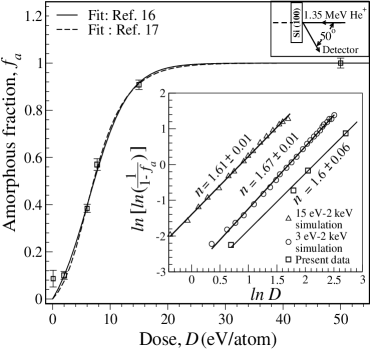
For quantitative analysis, the amorphized fraction, , for a given fluence , was determined from the surface peak intensity in RBS/C data, relative to a virgin sample. This value was normalized to unity at the highest fluence (corresponding to complete amorphization). Since Al5, Si5 and Cs are different systems we convert the fluence, to dose, (eV/atom). This is done using the equation, , , and representing the projected range of the implanted atom, its energy and the atomic density of the matrix ( cm-3) respectively. Since the clusters break almost immediately upon impact, the damage produced due to their implantation is mainly due to 5 or 6 keV Si or Al atoms respectively which have ranges of 10.2 and 12.7 nm in Si trim . Based on TEM data (shown later), for Si and Cs atoms, we take the ranges to be 10 nm and 20 nm respectively. The results are shown in Fig. 1. The 95% level in is seen to occur at a dose of eV/atom, complete saturation occurring around 20 eV/atom. This is higher than the saturation value of 6-12 eV/atom as indicated by simulations nordlund2 .
The results can be explained in terms of a combined Direct impact and defect stimulated mechanism hecking . This is mainly because presence of defects is known to result in a faster growth in the amorphized fraction bai ; holland . The cross-section for the defect stimulated process, , depends on the same for the direct impact process, . In such a case, weber . A fit to the data yields values of 0.254 ( 0.012) and 0.04 ( 0.005) for and respectively.
To look at cascade overlap effects we have used the Cascade quenching and recrystallization model proposed by Wang et al wang . Here amorphization is assumed to be the result of direct impact of energetic ions, however, under a competing effect of partial recrystallization. Using a recrystallization efficiency, , one can write , where , represents a dimensionless normalized dose. The parameter is related to the cross sectional area of the damaged region at any given dose. A fit using the above model yields a value of 0.893 () for , together with a value of 2.214 (). This value indicates, on an average, a 5 keV Si atom generates damage in a cylindrical region of cross sectional area of 22 nm2 calc , corresponding to a track radius of nm. Now we look at our fit values against the simulation results of Nord et al nordlund2 (as given in their table-IV). In our case saturation occurs at 20 eV/atom indicating a normalized dose, of about 44. With almost identical values, simulations for the two cases viz with 3 eV - 2.0 keV and 15 eV - 2 keV recoils, show values of 3.822 and 6.326 respectively. The corresponding values of 12 eV/atom and 6.5 eV/atom result in very similar values of 45.86 and 41, in good agreement with present data. A value of 44 indicates a complete amorphisation at a of atoms-cm-2 in good agreement with earlier data bai .
The growth in with dose, , can also be studied using a Nucleation and growth model based on the KJMA equation kjma of the form . Here is related to the nucleation rate (dependent on ) while is related to the growth velocity (dependent on ), at the interface weber . The Avrami exponent, , as determined from the slope of vs (Fig. 1) yields a value 1.6 (close to 3/2), indicating a diffusion limited nucleation and growth mechanism to be valid erukhi . Simulation results of Nord et al, nordlund2 , for realistic (variable energy) recoil distributions, yield very similar values (Fig. 1) in agreement with our findings. This is in contrast to some earlier results on Ge induced amorphisation of Si carried out at higher energies, where was shown to be 3.5 campisano . Since has almost the same value in both simulated and experimental data, different values indicates unequal growth velocities at the a/c interface.
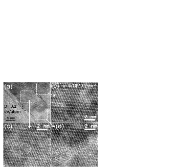
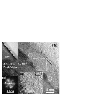
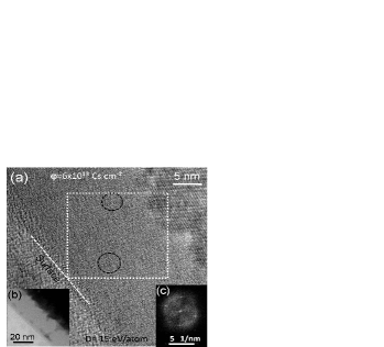
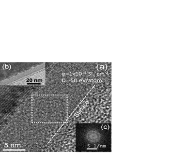
Fig. 2 (a) shows an XTEM picture of the defected region as obtained for an Si5 fluence of cm-2, corresponding to a dose, , of 0.2 eV/atom. Fig. 2(b) corresponds to an undamaged region. Fig. 2(c) & (d) show defects in the form of an amorphized patch and dislocations respectively, present within a depth of 10 nm (range of 5 keV Si in Si). HR XTEM images for the sample implanted with Si5 fluence of cm-2 (dose eV/atom) are shown in Fig. 3 (a) & (b). In this case a heavily damaged region, extending from the ion end-of-range (EOR) up to the surface, can be seen. One can notice a rough interface together with a lot of crystalline patches in the near surface region. This is due to spatial overlap of collision cascades at the ion EOR where a high density of low energy recoils is expected to be produced. A Fourier transformed (FT) image of a 10 nm size region (Fig. 3 (c)) shows diffused -diffraction spots along with shifted lobes indicating incomplete amorphisation and strain in the system. A Fourier inversion of the diffraction image (Fig. 3(d)) clearly shows the heavily damaged lattice with misoriented planes. One can also see some amorphized patches (shown in circles) in the damaged region. Compared to this, the XTEM images for the Cs implantation case (Fig. 4 (a) & (b)), for a dose of eV/atom, show a greater degree of amorphization. The FT image (Fig. 4 (c)), of a damaged patch as marked, shows a continuous ring indicating a largely amorphized layer. The direct image also shows this, however, with some crystalline patches still present. The corresponding fluence for 5 keV Si in Si, cm-2, is very close to the threshold for amorphisation (the 95% level occurs at 17.5 eV/atom). But the interface is still very rough. HR XTEM images of the damaged region obtained with an Si5 implantation fluence of cm-2 are shown in Fig. 5 (a)&(b). This case corresponds to a dose of about 50 eV/atom which is well above the amorphization threshold. Fig. 5(a) shows complete amorphization, the diffraction image (Fig. 5(c)) of a representative marked region showing two clear rings. The a/c interface is also seen to be rather flat, mainly due to stress relaxation volkert .
The above observations can be explained as follows. Si (or Al) atoms at 5 (or 6 keV) or 25 keV Cs atoms, in addition to creating point defects, produce amorphous patches in the implanted region. Some of these, are seen in Fig. 2(c). With increase in dose, with larger overlap of collision cascade regions there is a growth in the amorphized volume extending from the EOR towards the surface. Fig. 3 and Fig. 4 show this, with chunks of crystalline material present near the surface. These crystalline regions finally get amorphized from impact of low energy recoils due to successive ion passes. However, the growth in amorphisation is diffusion limited as the Avrami exponent, , has a value close to 3/2 kjma . We believe, the above diffusion limited growth mechanism also holds for amorphisation near the EOR. In this case the rough interface is smoothed out because of the depth limit imposed by the ion energy in addition to stress relaxation.
For most of the potentials used for simulation of the Si structure, an energy deposition of 6-8 eV/atom is needed for getting an amorphous structure nordlund2 . This is small compared to the amorphizing dose ( eV/atom), as obtained here. One of the reasons could be that the experiments were carried out at room temperature () where small amorphous patches can get recrystallized even without any ion passage delaRubia , leading to a smaller growth rate. Another reason could be a possible underestimation of the recrystallization effects due to keV energy recoils in the simulation. At higher beam energies and higher beam currents, amorphisation will be suppressed by recrystallization induced by relatively larger number of recoils, pushing the amorphization threshold to a higher dose. This could be the reason behind getting an amorphization threshold of cm-2, with 230 keV Si bai , as compared to almost half that in the present case. Beam energy and current induced annealing effects may even result in recrystallization of amorphous patches leading to the formation of point defects and related complexes delaRubia ; santos . In case the concentration such defects becomes too high homogeneous amorphization may take place. This does not happen in the present case.
To conclude, using 30 keV Al5, 25 keV Si and 25 keV Cs- ions, we have shown that ion induced amorphisation in Si, at low energy, is very much dependent on the direct impact mechanism resulting in heterogeneous amorphisation. At these energies, complete amorphisation seems to take place through a diffusion limited, nucleation and growth process.
We thank Prof. S. D. Mahanti, Michigan State University, East Lansing, USA and Prof. S. M. Bhattacharjee, IOP, Bhubaneswar for some critical comments and suggestions. We also thank the staff of the Ion Beam Laboratory, IOP, Bhubaneswar for their help during the experiments.
References
- (1) L. Pelaz, L. A. Marques and J. Barbolla, J. Appl. Phys. 96, 5947 (2004) and references therein.
- (2) J. Nord, K. Nordlund and J. Keinonen, Phys. Rev. B 65, 165329 (2002) and references therein.
- (3) F. F. Morehead, Jr. and B. L. Crowder, Radiat. Eff. 6, 27 (1970).
- (4) M. O. Roult, J. Choumont, J. M. Penisson and A. Bourret, Philos. Mag. A 50, 667 (1984).
- (5) L. M. Howe and M. H. Rainville, Nucl. Instrum. Methods 182/183, 143 (1981)
- (6) J. Narayan, D. Fathy, O. S. Oen and O. W. Holland, J. Vac. Sci. Technol. A 2, 1303 (1984), J. Narayan, O. S. Oen, D. Fathy and O. W. Holland, Mater. Lett. 3, 67 (1985)
- (7) L. A. Marques, L. Pelaz, J. Hernandez and J. Barbolla, Phys. Rev. B 64, 045214(2001); L. A. Marques, L. Pelaz, P. Lopez, I. Santos and M. Aboy, Phys. Rev. B 76, 153201 (2007).
- (8) T. Motooka, S. Harada and M. Ishimaru, Phys. Rev. Lett. 78, 2980 (1997).
- (9) M. L. Swanson, J. R. Parsons and C. W. Hoelke, Radiat. Eff. 9 , 249 (1971).
- (10) G. Bai and M. -A. Nicolet, J. Appl. Phys. 70, 648 (1991).
- (11) O. W. Holland and S. J. Pennycook, Appl. Phys. Lett. 55, 2503 (1989).
- (12) H. P. Lenka, B. Joseph, P. K. Kuiri, G. Sahu, P. Mishra, D. Ghosh and D. P. Mahapatra, J. Phys. D: Appl. Phys. 41, 315305 (2008).
- (13) A. N. Kolmogorov, Bull. Acad. Sci. USSR 3, 355 (1937); English translation: Selected Works of A. N. Kolmogorov, edited by A. N. Shiryayev Kluwer, Dordrecht, 1992, Vol. 2, p. 188, W. A. Johnson and R. F. Mehl, Trans. Am. Inst. Min. (Metall.)Eng. 135, 416 (1939); M. Avrami, J. Chem. Phys. 7, 1103 (1939).
- (14) M. K. El-Gohr, O. W. Holland, C. W. White and S. J. Pennycook, J. Mater. Res. 5, 352 (1990).
- (15) J. F. Ziegler, J. P. Biersack and U. Littmark, The Stopping and Range of Ions in Matter (Perganon Press, New York, 1995).
- (16) N. Hecking, K. F. Heidemann and E. T. Kaat, Nucl. Instrum. Methods Phys. Res. B 15, 760 (1986);
- (17) S. X. Wang, L. M. Wang and R. C. Ewing, Phys. Rev. B 63, 024105 (2001).
- (18) W. J. Weber, Nucl. Instrum. Methods Phys. Res. B 166/167, 98 (2000).
- (19) For any , deviding by one can determine the cross sectional area of the ion track. needs to be calculated taking the appropriate and .
- (20) V. Erukhimovitch and J. Baram, Phys. Rev. B 51, 6221 (1995).
- (21) S. U. Campisano, S. Coffa, V. Raineri, P. Priolo and E. Rimini, Nucl. Instrum. Methods Phys. Res. B 80/81, 514 (1993).
- (22) L. J. Lewis and R. M. Nieminen, Phys. Rev. B 54, 1459 (1996).
- (23) C. A. Volkert, J. Appl. Phys. 70, 3521 (1991).
- (24) I. Santos, L. -A. Marques and L. Pelaz, Phys. Rev. B 74, 174115 (2006).
- (25) T Diaz dela Rubia and G. H. Gilmer, Phys. Rev. Lett. 74, 2507 (1995).