Energy gaps in etched graphene nanoribbons
Abstract
Transport measurements on an etched graphene nanoribbon are presented. It is shown that two distinct voltage scales can be experimentally extracted that characterize the parameter region of suppressed conductance at low charge density in the ribbon. One of them is related to the charging energy of localized states, the other to the strength of the disorder potential. The lever arms of gates vary by up to 30% for different localized states which must therefore be spread in position along the ribbon. A single-electron transistor is used to prove the addition of individual electrons to the localized states. In our sample the characteristic charging energy is of the order of 10 meV, the characteristic strength of the disorder potential of the order of 100 meV.
pacs:
71.15.Mb, 78.30Na, 81.05.Uw, 63.20.KrGraphene nanoribbons che07 ; han07 ; dai08 ; wan08 ; lin08 and narrow graphene constrictions sta08a ; pon08 ; sta08b display unique electronic properties based on truly two-dimensional (2D) graphene gei07 with potential applications in nanoelectronics kat07 and spintronics tra07 . Quasi-1D graphene nanoribbons and constrictions are of interest due to the presence of an effective energy gap, overcoming the gap-less band structure of graphene and leading to overall semiconducting behavior, most promising for the fabrication of nanoscale graphene transistors wan08 , tunnel barriers, and quantum dots sta08a ; sta08b ; pon08 . On the other hand, ideal graphene nanoribbons bre06 ; whi07 promise interesting quasi-1D physics with strong relations to carbon nanotubes rei03 . Zone-folding approximations whi07 , -orbital tight-binding models per06 ; dun07 , and first principle calculations fer07 ; yan07a predict an energy gap scaling as with the nanoribbon width , where ranges between 0.2–1.5 eVnm, depending on the model and the crystallographic orientation of the nanoribbon lin08 . However, these theoretical estimates can neither explain the experimentally observed energy gaps of etched nanoribbons of widths beyond 20 nm, which turn out to be larger than predicted, nor do they explain the large number of resonances found inside the gap che07 ; han07 ; sta08b . This has led to the suggestion that localized states (and interactions effects) due to edge roughness, bond contractions at the edges son08 and disorder may dominate the transport gap.

Several mechanisms have been proposed to describe the observed gap, including re-normalized lateral confinement han07 , quasi-1D Anderson localization muc08 , percolation models ada08 and many-body effects (incl. quantum dots) sol07 , where substantial edge disorder is required. Recently, it has been shown that also moderate amounts of edge roughness can substantially suppress the linear conductance near the charge neutrality point hei08 , giving rise to localized states relevant for both single particle and many-body descriptions.
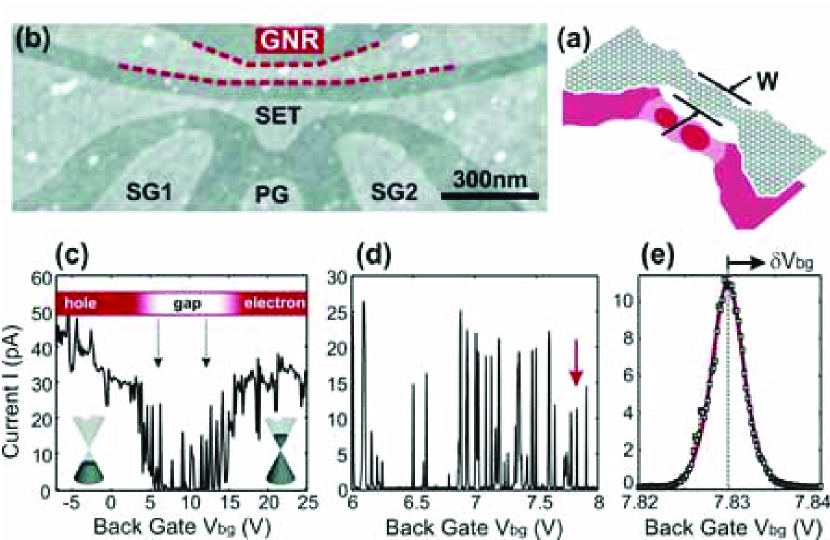
In this paper we show experimental evidence that the transport gap in an etched graphene nanoribbon (see schematic in Fig. 1a) is primarily formed by local resonances and quantum dots along the ribbon. We employ lateral graphene gates to show that size and location of individual charged islands in the ribbon vary as a function of the Fermi energy. In addition, we use a graphene single electron transistor (SET) to detect individual charging events inside the ribbon.
We focus on an all-graphene setup, as shown in Fig. 1b, where a nanoribbon (highlighted by dashed lines) with nm is placed at a distance of 60 nm from a graphene SET with an island diameter of 200 nm. The back gate (BG) allows us to tune the overall Fermi level and three lateral graphene gates mol07 , PG, SG1 and SG2 are used to locally tune the potential of the nanoribbon and the SET. The sample fabrication is based on mechanical exfoliation of graphite nov04 , electron beam lithography, reactive ion etching and evaporation of Ti/Au contacts. A detailed description is found in Refs. dav07a, ; mol07, , and sta08a, . The device is measured in two-terminal geometry by low frequency lock-in techniques in a variable temperature insert cryostat at a temperature of 1.7 K.

Fig. 1c shows the low source–drain bias ( = 300 V ) back-gate characteristic of the nanoribbon,where we tune transport from the hole (left side) to the electron regime. The region 6 V 12 V of suppressed current (marked by two arrows) is the so-called transport gap in back gate voltage ( 6 V). In contrast to the energy gap predicted for samples without disorder, where transport should be completely pinched-off, we observe—in good agreement with other experimental work che07 ; han07 ; sta08b —a large number of reproducible conductance resonances inside the gap.
A high-resolution close-up of Fig. 1c shown in Fig. 1d reveals a sequence of resonances with a small line-width indicating strong localization. A particularly narrow resonance is shown in Fig. 1e (see arrow in Fig. 1d). The line-shape can be well fitted by , where is the back gate lever arm and (see Fig. 1e) bee91 . The estimated effective electron temperature, 2.1 K, is close to the base temperature, leading to the conclusion that the peak broadening is mainly limited by temperature rather than by the life-time of the resonance.
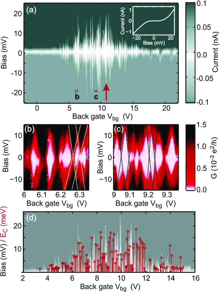
In Fig. 2a we show source–drain current measurements on the nanoribbon as a function of source–drain bias and back gate voltage (i.e., Fermi energy). We observe regions of strongly suppressed current (white areas) leading to an effective energy gap in bias direction inside the transport gap in back gate voltage (shown in Fig. 1c). Highly non-linear I-V characteristics (see e.g. inset in Fig. 2a) are characteristic for the energy gap in bias direction. This energy gap agrees reasonably well with the observations in Refs. han07, , and sol07, of an energy gap of 8 meV, for = 45 nm.
The transport gap in source–drain bias voltage corresponding to the energy gap , and the transport gap in back gate voltage are two distinct voltage scales resulting from our experiment. The quantity is measured at constant (nearly zero) (transport window) but varying Fermi energy and is related to a change in Fermi energy in the system. Varying the magnitude of the transport window at fixed Fermi energy gives rise to .
We estimate the energy scale corresponding to from , (where is the back gate capacitance per area) com01a . We find an energy gap meV which is more than one order of magnitude larger than . We attribute this discrepancy to different physical meanings of these two energy scales, which will be further illustrated and discussed below.
More insight into the two energy scales and their relation is gained by focusing on a smaller back gate voltage range as shown in Figs. 2b,c which are two high resolution differential conductance close-ups of Fig. 2a (see labels therein). At this scale transport is dominated by well distinguishable diamonds of suppressed conductance (see bright areas and dashed lines in Figs. 2b,c) which indicate that transport is blocked by localized electronic states or quantum dots (see also Ref. mol08a ). The related charging energy which itself is related to the quantum dot size, depends on the Fermi energy on a small back gate voltage scale (see different diamond sizes in Figs. 2b,c), but also on a large scale (see Fig. 2a). In order to confirm this statement the extracted charging energies are plotted in Fig. 2d into the top half of the measurements shown in Fig. 2a.

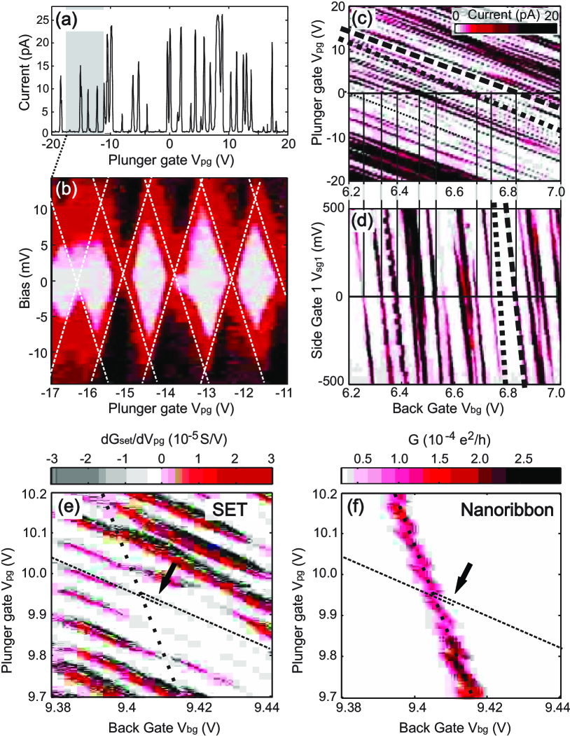
Figures. 3a,b show differential conductance measurements at fixed V, as a function of the lateral plunger gate voltage (c.f., Fig. 1b) which tunes the potential on the nanoribbon locally. Similar to the back gate dependent measurements in Fig. 1d we observe in Fig. 3a a large number of resonances inside the transport gap. In contrast to back gate sweeps we find certain plunger gate regions with almost equally spaced conductance peaks (see, e.g., the highlighted regime in Fig. 3a and the corresponding diamonds in Fig. 3b), giving rise to the assumption that here only a single charged island is tuned by the lateral gate. These diamond measurements are of comparable quality as those presented in Refs. sta08a ; pon08 ; sta08b .
By following resonances at low bias () over a larger range (see Fig. 3c) we observe that individual resonances exhibit different relative lever arms in the range of (slopes of dotted and dashed lines in Fig. 3c). These variations of up to 20 can be attributed to different capacitances between the plunger gate and individual electron puddles, which sensitively includes their local position on the ribbon. By sweeping the voltage on the more asymmetrically placed side gate 1 (see Fig. 1b) rather than the plunger gate this effect is even enhanced. In Fig. 3d we show the corresponding measurements ( = 0 V). Relative lever arms in the range of with scattering of more than 30 can be extracted. The stability of the sample allows to match resonances seen in Figs. 3c and 3d so that they can be followed in a 3D parameter space. These measurements confirm local resonances being located along the nanoribbon, with different lever arms to the local lateral gates.
We now make use of the SET device fabricated near the ribbon to detect individual charging events inside localized states of the nanoribbon. The SET which has been characterized before gue08 , has a charging energy of meV and Coulomb blockade peak spacing fluctuations below . The Coulomb resonances in the conductance of the SET, highlighted as dashed lines in Fig. 3e can be used to detect charging of a local resonance (dotted line in Fig. 3e) in the nanoribbon with individual electrons. We show conductance measurements as function of plunger and back gate voltage in order to identify resonances of the SET and the nanoribbon via their different relative lever arms (Figs. 3e,f). Since the SET is much closer to the PG than the nanoribbon, the relative lever arm 0.18 seen as the slope of SET resonances in Fig. 3e (dashed lines in Figs. 3e,f) is significantly larger than the relative lever arm of a resonance in the nanoribbon 0.04 shown in Fig. 3f (dotted lines in Figs. 3e,f). The observation of a jump (see arrow in Fig. 3e) in the Coulomb resonances of the SET when they cross the resonance in the ribbon is a clear signature of charging the localized state in the nanoribbon, which changes in a discontinuous way the potential on the SET island by capacitive coupling. This shows that we accumulate localized charges along the nanoribbon as function of the back gate voltage.
The experimental data shown above provide strong indications that the two experimentally observed energy scales and are related to charged islands or quantum dots forming spontaneously along the nanoribbon. This is supported by the observation (i) of Coulomb diamonds, which vary in size as function of the Fermi energy, (ii) of a strong variation of the relative lever arms of individual resonances and (iii) of local charging of islands inside the nanoribbon.
Quantum dots along the nanoribbon can arise in the presence of a quantum confinement energy gap () combined with a strong bulk and edge-induced disorder potential , as illustrated in Fig. 4. The confinement energy can be estimated by , where eV and nm whi07 . This leads to meV for nm, which by itself can neither explain the observed energy scale , nor the formation of quantum dots in the nanoribbon. However, by superimposing a disorder potential giving rise to electron-hole puddles near the charge neutrality point mar07 , the confinement gap ensures that Klein tunneling (from puddle to puddle) gets substituted by real tunneling. Within this model depends on both the confinement energy gap and the disorder potential. An upper bound for the magnitude of the disorder potential can be estimated from our data to be given by . Comparing to Ref. mar07 where a bulk carrier density fluctuation of the order of cm-2 was reported, we find reasonable agreement as the corresponding variation of the local potential is meV.
We can estimate the fraction of overlapping diamonds by summing over all charging energies observed in Fig. 2d. This leads to 630 meV. Comparison with the estimate for gives 45 - 82 overlapping diamonds. We expect that this value depends strongly on the length of the nanoribbon in agreement with findings of Ref. mol08a .
The energy gap in bias direction does not tell much about the magnitude of the disorder potential, but it is rather related to the sizes of the charged islands. In particular, the minimum island size is related to the maximum charging energy . By using a simple disc model we can estimate the effective charge island diameter by nm (where ), which exceeds the nanoribbon width . Thus, in ribbons of different width the charging energy will scale with giving the experimentally observed dependence of the energy gap in bias direction han07 .

In conclusion, we have presented detailed transport measurements on a graphene nanoribbon, focusing on the origin of the transport gap. Experimentally we find two distinct energy scales characterizing this gap. The first of them is the charging energy of local resonances or quantum dots forming along the ribbon. The second is probably dominated by the strength of the disorder potential, but also dependent on the gap induced by confinement due to the ribbon boundaries. These insights are important to understand transport in graphene nanostructures and may help in designing future graphene nanoelectronic components.
Acknowledgment — The authors wish to thank A. Castro-Neto, S. Das Sarma, T. Heinzel, M. Hilke, F. Libisch, K. Todd and L. Vandersypen for helpful discussions. Support by the Swiss National Science Foundation and NCCR nanoscience are gratefully acknowledged.
References
- (1) Z. Chen, Y.-M. Lin, M. Rooks and P. Avouris, Physica E, 40, 228, (2007).
- (2) M. Y. Han, B. Özyilmaz, Y. Zhang, and P. Kim, Phys. Rev. Lett., 98, 206805 (2007)
- (3) X. Li, X. Wang, L. Zhang, S. Lee, H. Dai, Science, 319, 1229 (2008).
- (4) Y.-M. Lin, V. Perebeinos, Z. Chen and P. Avouris, arXiv:080xx0035v2 (2008)
- (5) X. Wang, Y. Ouyang, X. Li, H. Wang, J. Guo, and H. Dai, Phys. Rev. Lett., 100, 206803 (2008)
- (6) C. Stampfer, J. Güttinger, F. Molitor, D. Graf, T. Ihn, and K. Ensslin, Appl. Phys. Lett., 92, 012102 (2008)
- (7) L. A. Ponomarenko, F. Schedin, M. I. Katsnelson, R. Yang, E. H. Hill, K. S. Novoselov, A. K. Geim, Science, 320, 356 (2008).
- (8) C. Stampfer, E. Schurtenberger, F. Molitor, J. Güttinger, T. Ihn, and K. Ensslin, Nano Lett., 8, 2378 (2008)
- (9) A. K. Geim and K. S. Novoselov, Nat. Mater. 6, 183 (2007).
- (10) M. I. Katnelson, Materials Today 10(1-2), 20 (2007)
- (11) B. Trauzettel, D.V. Bulaev, D. Loss, and G. Burkard, Nature Physics, 3, 192, (2007).
- (12) L. Brey and H. A. Fertig, Phys. Rev. B, 73, 235411 (2006).
- (13) C. T. White, J. Li, D. Gunlycke, and J. W. Mintmire, Nano Lett., 7, 825 (2007).
- (14) For review on carbon nanotubes see e.g.: S. Reich, C. Thomsen, J. Maultzsch, ”Carbon Nanotubes”, Wiley-VCH, 2003.
- (15) N. M. R. Peres, A. H. Casrtro Neto and F. Guinea, Phys. Rev. B, 73, 195411 (2006).
- (16) D. Dunlycke, D. A. Areshkin, and C. T. White, Appl. Phys. Lett., 90, 142104 (2007).
- (17) J. Fernandez-Rossier, J .J. Palacios, and L. Brey, Phys. Rev. B, 75, 205441 (2007).
- (18) L. Yang, C.-H. Park, Y.-W. Son, M. L. Cohen, and S. G. Louie, Phys. Rev. Lett., 99, 186801 (2007).
- (19) F. Sols, F. Guinea and A. H. Castro Neto, Phys. Rev. Lett., 99, 166803 (2007).
- (20) Y.-W. Son, M. L. Cohen, and S. G. Louie, Phys. Rev. Lett., 99, 186801 (2007).
- (21) E. R. Mucciolo, A. H. Castro Neto and C. H. Lewenkopf, arXiv:0806.3777v1 (2008).
- (22) S. Adam and S. Cho and M. S. Fuhrer and S. Das Sarma, Phys. Rev. Lett., 101, 046404 (2008).
- (23) M. Evaldsson, I. V. Zozoulenko, Hengyi Xu, T. Heinzel, arXiv:0805.4326 (2008).
- (24) F. Molitor, J. Güttinger, C. Stampfer, D. Graf, T. Ihn, and K. Ensslin, Phys. Rev. B 76, 245426 (2007).
- (25) K. S. Novoselov, A. K. Geim, S. V. Morozov, D. Jiang, M. I. Katsnelson, S. V. Dubonos, I. V. Grigorieva, A. A. Firsov, Science, 306, 666, (2004).
- (26) D. Graf, F. Molitor, K. Ensslin, C. Stampfer, A. Jungen, C. Hierold, and L. Wirtz, Nano Lett. 7, 238 (2007).
- (27) C. W. J. Beenakker, Phys. Rev. B 44, 1646 (1991).
- (28) F. Molitor et al., in preparation (2008).
- (29) Here we assume that the charge neutrality point is right in the center of the transport gap (9 V). Moreover, we make use of the following boundary conditions for . Lower bound: cm-2V. Upper bound: Following Ref. lin08 the ratio increases with decreasing , where is the oxide thickness, and we obtain = 30 nm 10 .
- (30) J. Güttinger, C. Stampfer, S. Hellmüller, F. Molitor, T. Ihn, and K. Ensslin, arXiv:0809.3904 (2008)
- (31) J. Martin, N. Akerman, G. Ulbricht, T. Lohmann, J.H. Smet, K. von Klitzing, and A. Yacoby, Nature Physics, 4, 144 - 148 (2008).