Quantum Dot Behavior in Graphene Nanoconstrictions
Abstract
Graphene nanoribbons display an imperfectly understood transport gap. We measure transport through nanoribbon devices of several lengths. In long (250 nm) nanoribbons we observe transport through multiple quantum dots in series, while shorter (60nm) constrictions display behavior characteristic of single and double quantum dots. New measurements indicate that dot size may scale with constriction width. We propose a model where transport occurs through quantum dots that are nucleated by background disorder potential in the presence of a confinement gap.
Stanford University Department of Physics] Department of Physics, Stanford University, Stanford, California, 94305, USA Department of Applied Physics] Department of Applied Physics, Stanford University, Stanford, California, 94305, USA Stanford University Department of Physics] Department of Physics, Stanford University, Stanford, California, 94305, USA Stanford University Department of Physics] Department of Physics, Stanford University, Stanford, California, 94305, USA
Graphene is a two-dimensional conductor with remarkable properties ranging from long spin relaxation times [Tombros et al.(2007)Tombros, Jozsa, Popinciuc, Jonkman, and van Wees] to very high mechanical strength [Booth et al.(2008)Booth, Blake, Nair, Jiang, Hill, Bangert, Bleloch, Gass, Novoselov, Katsnelson, , and Geim] to the highest known room temperature mobilities [Bolotin et al.(2008)Bolotin, Sikes, Jiang, Klima, Fudenberg, Hone, Kim, and Stormer]. Extended graphene sheets also display a non-zero minimum conductivity even at nominally zero carrier densities, which limits their applicability for some types of semiconductor devices such as transistors with high on-off ratios. When graphene is etched into narrow strips known as nanoribbons, however, conductance through the device is suppressed for a wide range of Fermi energies around the Dirac point. The observation of this conduction gap,[Han et al.(2007)Han, Özyilmaz, Zhang, and Kim, Chen et al.(2007)Chen, Lin, Rooks, and Avouris, Li et al.(2008)Li, Wang, Zhang, Lee, and Dai] which scales inversely with ribbon width,[Han et al.(2007)Han, Özyilmaz, Zhang, and Kim] has led to the proposal of graphene nanoribbons as next-generation high-frequency transistors. However, the observed conduction gaps are larger than those expected from a single-particle confinement picture in the absence of lattice effects at the edges, while studies on nanoribbons of different orientations with respect to the graphene lattice[Han et al.(2007)Han, Özyilmaz, Zhang, and Kim] demonstrate that explanations depending on the presence of well-defined crystallographic edges[Son et al.(2006)Son, Cohen, and Louie, Brey and Fertig(2006), Yang et al.(2007)Yang, Park, Son, Cohen, and Louie] do not apply. Several alternative explanations have been put forward to explain the large energy scale of the conduction gap. One proposal involves a non-conductive "dead zone" at the ribbon edges due to atomic-scale disorder that causes the effective conducting ribbon width to be narrower than the physical width[Han et al.(2007)Han, Özyilmaz, Zhang, and Kim]. Elaborations on this idea propose that atomic-scale disorder near the ribbon edge may give rise to localized states that extend into the ribbon body[Evaldsson et al.(2008)Evaldsson, Zozoulenko, Xu, and Heinzel]. Conversely, random charged impurity centers in the body of the ribbon, in combination with the ribbon’s confinement gap, have been proposed to cause a metal-insulator transition[Adam et al.(2008)Adam, Cho, Fuhrer, and Das Sarma]. Others have suggested that lithographic line edge roughness may create a series of quantum dots defined by nanometer-scale variations in ribbon width[Sols et al.(2007)Sols, Guinea, and Castro Neto]. Here we examine detailed conduction characteristics of long nanoribbons as well as short nanoconstrictions in an attempt to elucidate the origin of the large conduction gap in graphene nanoribbons. In light of our data, we propose that the random charged impurity centers present throughout the graphene sheet, in conjunction with a gap stemming from the constriction’s confined geometry, give rise to isolated puddles of charge carriers acting as quantum dots both in long nanoribbons and in short nanoconstrictions, even in cases where the constriction length is so short that there is no hard transport gap. The physical origin of quantum dot behavior in graphene nanoribbons has implications for the manufacture of graphene nanoribbon transistors.
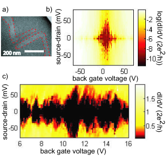
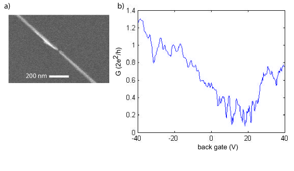
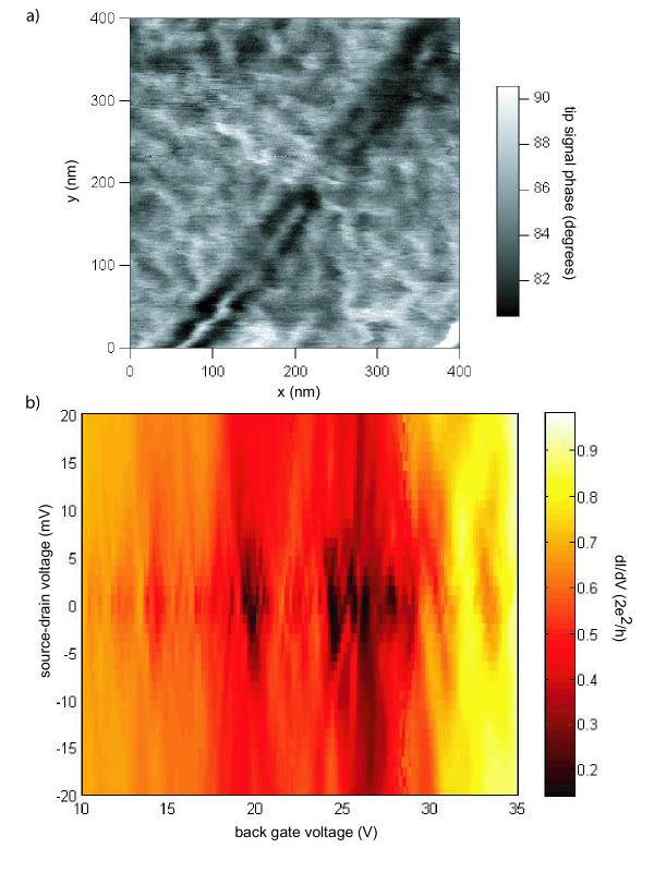
As reported elsewhere [Han et al.(2007)Han, Özyilmaz, Zhang, and Kim, Chen et al.(2007)Chen, Lin, Rooks, and Avouris], long (1 micron) graphene nanoconstrictions display gapped behavior: conduction is suppressed by several orders of magnitude for a wide range of gate voltages around the Dirac point, and for tens of mV of source-drain bias. In 1 we show data from a 250 nm long, 40 nm wide graphene nanoribbon patterned by oxygen plasma etching through a PMMA mask on a graphene flake. This flake and all others discussed in this paper have been verified to be single-layer by Raman spectroscopy[Ferrari et al.(2006)Ferrari, Meyer, Scardaci, Casiraghi, Lazzeri, Mauri, Pisanec, Jiang, Novoselov, Roth, and Geim, Graf et al.(2007)Graf, Molitor, Ensslin, Stampfer, Jungen, Hierold, and Wirtz], and are contacted by Ti/Au metal patterned far from the constriction region. We estimate the flake mobility to be 500 cm/Vs based on two-wire measurements made between contacts not spanning the constriction.\bibnoteBecause two-wire measurements do not allow us to eliminate the effects of contact resistance, we base our mobility estimates on the slope of conductance traces at relatively low densities 10 V from the Dirac point where the graphene sheet resistance is still dominant over the contact resistances. All data reported herein are from two-probe measurements: in general the constriction resistance is larger than any other resistance in the circuit, and in any case four-probe measurements cannot eliminate the resistance of the region of the graphene flake between the metal contacts and the constriction region. We see the large scale gap reported by others (Figure 1b).[Han et al.(2007)Han, Özyilmaz, Zhang, and Kim, Chen et al.(2007)Chen, Lin, Rooks, and Avouris] Careful examination of the conduction inside the gapped region (Figure 1c) reveals Coulomb diamond-like features, with conduction suppressed by more than 7 orders of magnitude around zero source-drain voltage for nearly all gate voltages, indicating the presence of several quantum dots in series. From the dI/dV map we calculate dot areas ranging from 860 to 1700 nm, consistent with the formation of dots that span the width of the ribbon, with lengths of the same order as their widths. \bibnoteWe calculate dot size based on a parallel plate capacitor model where the back gate defines one plate of the capacitor and the graphene sheet and nearby metal gates define the other plate, justified by the presence of conducting graphene sheet everywhere except for the two narrow strips defining the constriction. The presence in each of the samples discussed here of graphene or metal gates near the constriction may result in some screening of the back gate voltage, resulting in an underestimation of dot areas in each case. In data sets where dI/dV is measured with respect to side gate voltage, we calculate an equivalent back gate voltage using a separately measured multiplier. In the course of the paper we use the same method to calculate dot sizes in nanoconstrictions of varying width and length. We summarize the sample dimensions, mobilities and dot sizes in 1.
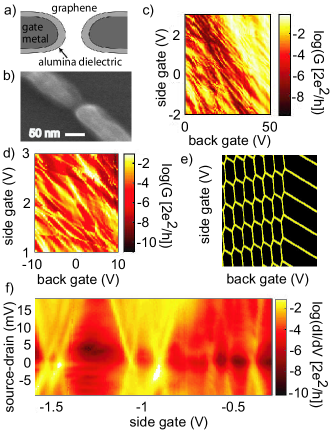
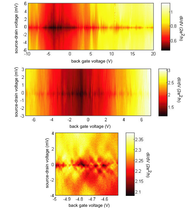
In order to better understand the origin of these quantum dots in long nanoribbons, we have fabricated a series of shorter (60 nm) constrictions: in doing so we hoped to isolate a small number of dots in the constriction region and study their behavior in detail. Fabrication of our short constrictions begins as for our long constrictions with the deposition of Ti/Au contacts on a graphene flake far from the constriction region and an oxygen plasma etch through a PMMA mask to define the constriction. In most of our short constrictions, however, this step is followed by the deposition of an aluminum oxide insulator and then gate metal, and finally liftoff, resulting in a nanoconstriction situated between two separately addressable side gates. In 2 we show data from a 60 nm long, 15 nm wide constriction. We estimate the mobility of the flake far from the constriction region to be 700 cm/Vs, although we emphasize that the processing steps that the constriction region has undergone in our side-gated constrictions may cause its mobility to differ from the mobility of the flake as a whole. Conductance traces with respect to back gate voltage show a wide region of suppressed conductance punctuated by narrow conductance peaks. A stability diagram (Figure 2c) of conductance versus back gate and one side gate exhibits features moving with a constant slope. From this slope we extract a measure of the relative capacitance of the side and back gates to the graphene in the constriction region. We identify the diagonal region of lowest average conductance running through the center of figure 2c as the set of back and side gate voltage pairs that bring the potential inside the constriction to the Dirac point. Within this diagonal region we observe relatively narrow and straight conductance peaks running in parallel. This region of simple conductance peaks, where conductance depends only on a single variable (the Fermi energy inside the constriction), is indicative of the presence of a single quantum dot, while outside the central Dirac region (see zoom in, Figure 2d) conductance peaks bend and exhibit hexagonal patterns characteristic of two or more quantum dots. We include a cartoon of the pattern expected from an idealized double-quantum dot system with a transition to single-dot behavior (Figure 2e).\bibnoteThe model we use to generate the expected double-dot behavior does not take into account the change in Fermi level with gate voltage that takes place in our system.
We measure nonlinear conductance across the constriction versus side gate voltage and source-drain bias (Figure 2f), setting the back gate to a constant 30 V so that the side gate accesses the Dirac point at approximately 0 V. At side gate voltages V near 0 V, we observe quasi-periodic Coulomb diamonds which all share similar heights in source-drain voltage, indicating that each diamond is produced by a state with the same total capacitance: in other words, reflecting the presence of a single quantum dot. At values of V below -1.1 V, a side gate voltage similar to that at which we observe a transition from single- to double-dot behavior in Figure 2d, the differential conductance pattern changes: we observe tall diamonds that intersect to form a small diamond at V = -1.5 V, suggesting that conduction is occurring through two quantum dots in parallel. From the spacing in gate voltage of the conductance peaks defining the uniform diamonds near the Dirac point and from the larger diamonds at higher V we calculate dot areas of 900 nm +/-70 nm for the single, larger dot near the Dirac point and 300 nm +/- 20 nm for the second, smaller dot at larger gate voltages \bibnoteThe uncertainties come largely from the conversion from side gate to equivalent back gate voltage. Excited state features with energy spacing of 7 meV can be seen running in parallel with the diamond boundaries in the diamond centered at V = -1.0 V in Figure 2f, along with inelastic cotunneling features in the diamond centered at -1.3 V (horizontal lines spanning the diamond). Excited state features as well as inelastic cotunneling features demonstrate the presence of two distinct energy scales. The existence of two distinct energy scales in our diamonds is enough alone to establish that these features are not conduction resonances stemming from transport through a single tunnel barrier. To rule out the possibility that the features are due to Fabry-Perot-like transport through double- or multiple barriers, we consider the energy scales involved. In a system such as this, with very low average conductance and therefore opaque tunnel barriers, Fabry-Perot transport would be equivalent to transport through a very large confined area, one so large that the charging energy has become negligible. The energy scales we observe in our device, however, are non-negligible: our diamond heights ( 4-20 mV) are in fact larger than those measured in many lithographically defined graphene quantum dots [Ponomarenko et al.(2008)Ponomarenko, Schedin, Katsnelson, Yang, Hill, Novoselov, and Geim, Stampfer et al.(2008)Stampfer, Güttinger, Molitor, Graf, Ihn, and Ensslin] where the existence of a non-negligible charging energy is well-established. We therefore conclude that the two energy scales we observe are the charging energy required to add an additional electron to the dot and the spacing of confinement energy levels inside the dot. The presence of inelastic cotunneling features is a further indication of transport through a quantum dot, as they stem from energy dissipation occurring inside the feature responsible for the conduction peaks, which is not possible inside a single simple tunnel barrier.
The dot size derived from our measured level spacing is inconsistent with energy level transitions in a circular quantum dot of the area calculated from the measured charging energy. Unlike experiments where quantum dots in graphene are geometrically defined[Stampfer et al.(2008)Stampfer, Güttinger, Molitor, Graf, Ihn, and Ensslin, Ponomarenko et al.(2008)Ponomarenko, Schedin, Katsnelson, Yang, Hill, Novoselov, and Geim], we have no measure of the shape (as opposed to the area) of the dot under study, and no reason to assume that it has a well-defined circular or square geometry. For more realistic geometries the Dirac spectrum produces chaotic level spacings from which it is not possible to extract geometric information without detailed statistics [De Raedt and Katsnelson(2008), Ponomarenko et al.(2008)Ponomarenko, Schedin, Katsnelson, Yang, Hill, Novoselov, and Geim]. From the side gate voltage where the larger diamond first appears, though, we estimate that the lowest energy level of this dot is located 100 meV from the Dirac point. We note that the bottom of the potential defining the dot does not necessarily coincide with the spatially averaged Dirac point measured by transport: however, should it be the case that the bottom of the potential defining the dot is not far from the spatially averaged Dirac point we calculate that this energy level corresponds to a length scale of 21 nm, which is in rough agreement with the size of this smaller quantum dot calculated from the spacings of Coulomb blockade peaks.
In order to gain information about localization lengths in narrow constrictions, we have fabricated on the same graphene flake a constriction of similar (10 nm) width but of 30 nm length. This very short constriction fails to show highly suppressed conductance near the Dirac point (see Figure 1 of the supplementary information). This is similar to the findings of Ponomarenko et al. [Ponomarenko et al.(2008)Ponomarenko, Schedin, Katsnelson, Yang, Hill, Novoselov, and Geim] regarding the necessity of fabricating very short constrictions at the entrances of their lithographically patterned graphene quantum dots in order to ensure large coupling to the leads. Based on our findings, we estimate that the localization length in our very narrow constrictions is on the order of 50 nm.
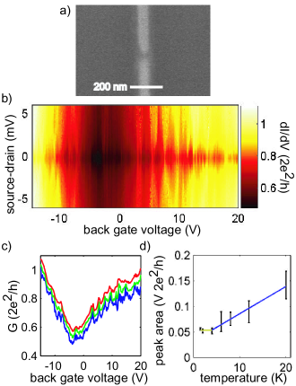
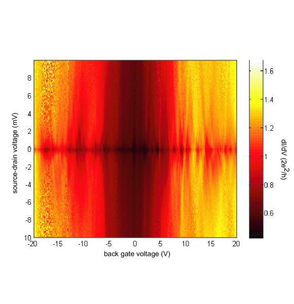
In contrast to the narrowest short constrictions, in short 60 nm long constrictions with widths of 35 and 55 nm, a regime where long nanoribbons (in work by us and others) [Han et al.(2007)Han, Özyilmaz, Zhang, and Kim, Chen et al.(2007)Chen, Lin, Rooks, and Avouris] show gapped conduction behavior at low temperatures, we do not observe a hard gap in transport. Instead, we measure conduction profiles similar to those observed in extended graphene sheets but with Coulomb diamond features overlaid. 3 shows data obtained from the 60 nm long, 35 nm wide constriction, patterned on a flake whose mobility we estimate to be 3000 cm/Vs. We address the question of whether the diamond features we observe reflect the presence of quantum dots or simply resonant tunneling through a barrier. In figure 3d we show the temperature dependence of the conductance peak area for the peak occurring at 6 V back gate voltage (V). In transport through a quantum dot a transition from a peak area that is constant in temperature to a peak area that increases linearly with increasing temperature should be observed when kT becomes comparable to the level spacing in the dot, corresponding to the transition between transport through single and multiple energy levels in the dot. Such a transition would also be observed in the case of resonant tunneling through a barrier, but it would occur at a temperature equivalent to the level spacing within the barrier: there would be no difference between the temperature at which this transition occurred and the "charging" energy measured in dI/dV. In our data, the temperature at which the transition from single-level to multi-level transport occurs is on the order of 4 K, or 0.7 meV, while the charging energy is greater than 5 meV for the peak in question. Another possibility is that the features we see in our source-drain maps reflect not Coulomb blockade but Fabry-Perot behavior. In fact we do observe Fabry-Perot features similar to those observed by Miao et al [Miao et al.(2007)Miao, Wijeratne, Zhang, Coskun, Bao, and Lau] but these features are much narrower than the Coulomb blockade features under discussion, disappear at temperatures above 1.5 K, and are also present in measurements made across contacts not spanning the constriction (see Figure 2 of the supplementary information). Because of these factors, we conclude that these small modulations on our large-scale Coulomb blockade features are associated with Fabry-Perot resonances occurring in the unpatterned graphene sheet between our contacts and the constriction. Having eliminated single-barrier and Fabry-Perot resonances as likely causes of the conductance patterns we observe in this constriction, we conclude that we are measuring conduction through a quantum dot.
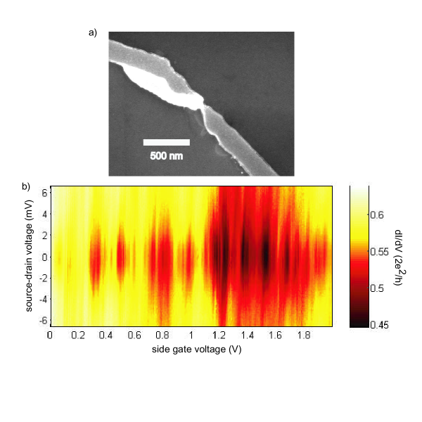
Calculation of the dot areas from conductance peak spacing in the 60 nm long, 35 nm wide constriction gives areas ranging from 400-600 nm, while the regular periodicity of the diamonds suggests single dot behavior in this region near the Dirac point. Diamond heights increase as the back gate voltage approaches the Dirac point, reflecting either a change in the capacitance of the dot to the source and drain due to the dot growing physically smaller as the Fermi energy approaches the Dirac point, or due to a change in the quantum capacitance of the dot as the density of states decreases near the Dirac point. Similar behavior is seen in a 60 nm long, 55 nm wide constriction (see Figure 3 of the supplementary information), where we find dot areas ranging from 1600 to 7100 nm. In 1 we summarize the calculated dot areas for all constrictions discussed here. Although more measurements would be necessary to make strong quantitative statements, the available data suggest that the area of quantum dots scales with the width but not the length of the constriction. We do not rule out the possibility that sample mobility may also play a role in determining dot size.
We emphasize that the 60 nm long, 35 nm wide constriction is narrower than the 250 nm long, 40 nm wide nanoribbon described in Figure 1, and yet displays Coulomb diamonds on top of a background that increases with gate voltage in a manner similar to bulk graphene instead of the hard-gapped conduction seen in long nanoribbons [Han et al.(2007)Han, Özyilmaz, Zhang, and Kim, Chen et al.(2007)Chen, Lin, Rooks, and Avouris]. This increasing background provides a possible explanation for why we do not observe a transition from single to multiple quantum dot behavior in wider constrictions: in these constrictions Coulomb blockade features at larger gate voltages would be obscured by the rising Dirac background.
The short length of our constrictions and their geometry (where the constriction is narrowest at its center) makes it implausible that quantum dot behavior in these constrictions stems from lithographic line edge roughness where the width of the ribbon varies randomly by a few nanometers over a length scale of tens of nanometers as has been proposed for long nanoribbons[Sols et al.(2007)Sols, Guinea, and Castro Neto]. In addition, we observe changes in differential conductance data (see Figure 4 of the supplementary information) after thermal cycling: the pattern of Coulomb diamonds becomes more complicated, suggesting multi- rather than single-dot transport, and the inferred dot size changes by factors of 2. These changes imply that a model where Coulomb blockade behavior is produced by line edge roughness alone does not apply.
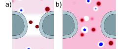
Instead we propose that the quantum dot behavior we observe in our samples may stem from the doping inhomogeneity of bulk graphene on [Martin et al.(2008)Martin, Akerman, Ulbricht, Lohmann, Smet, von Klitzing, and Yacoby], combined with the presence of a confinement gap from the constriction. The combination of these two effects would generate carrier-free regions at gate voltages near the Dirac point punctuated by islands of p- and n-type carriers: in 4 we show a cartoon based on simulations of the electron density induced by a gate voltage in combination with a random impurity potential landscape, where impurity density is extracted from sample mobility[Chen et al.(2008)Chen, Jang, Adam, Fuhrer, Williams, and Ishigami, Ando(2006), Nomura and MacDonald(2007), Cheianov and Fal’ko(2006), Hwang et al.(2007)Hwang, Adam, and Das Sarma]. Unlike more sophisticated treatments[Rossi and Das Sarma(2008), Lewenkopf and Castro Neto(2008)] our cartoon model does not take into account electron interaction effects in calculating the local electron density. After calculating the local potential due to the charged impurity landscape we impose a gap based on the confinement energy due the constriction and set the electron density to zero whenever the Fermi level plus the local potential is less than the gap. This procedure results in isolated puddles of electrons and holes embedded in an insulating environment for small gate voltages and narrow constrictions (Figure 4a) and a combination of isolated puddles and conducting regions spanning the constriction length for gate voltages farther from the Dirac point or wider constriction widths (Figure 4b). For more information about the generation of these cartoons, see the supplementary information. Experimental indications that dot size roughly scales with constriction width, but not with constriction length are consistent with our proposed model, and are inconsistent with the edge-defect model in a regime where localized states do not span the entire constriction width. It is likely that bulk mobility also plays a role in the size of dots formed in this scenario: future experiments will provide more quantitative information on the relationship between dot size, mobility and constriction width. In contrast to our model where bulk disorder is the most important factor in determining conductance properties of graphene nanoconstrictions, conduction gaps in long nanoribbons have in the past been explained in terms of Anderson localization caused by edge defects [Evaldsson et al.(2008)Evaldsson, Zozoulenko, Xu, and Heinzel, Mucciolo et al.(2008)Mucciolo, Castro Neto, and Lewenkopf]. In our short constrictions, the presence of nearby metal gates seems to pin the Dirac point in the ribbon at zero gate voltage, in contrast to our devices free of patterned metal gates where samples are generally p-type at zero gate voltage. Pinning, or alternatively screening effects from the nearby metal, may decrease the importance of edge disorder in our side-gated samples. In support of this proposal is the fact that data from samples fabricated in the same short-constriction geometry as those described above but without the deposition of metal gates on top of the etched area shows disordered differential conductance through the constriction with few identifiable Coulomb diamonds (see Figure 5 of supplementary information for an example of such a sample). We also emphasize that our measurements on short constrictions fabricated without metal side gates imply that our model, where bulk disorder effects dominate over edge effects, may be most applicable in devices with nearby patterned metal side gates. While we believe that bulk disorder should affect conductance through all constrictions, in constrictions fabricated without nearby metal gates effects associated with disordered edges might be more important. Local probe studies such as scanning gate microscopy on short constrictions patterned without metal side gates may in the future provide more information on the relative importance of bulk and edge disorder in non-side-gated constrictions and nanoribbons.
Supporting information is available: we describe our methods for generating the cartoons depicted in Figure 4, and we provide figures describing transport behavior through a 30 nm long, 10 nm wide constriction, low temperature Fabry-Perot behavior of a 60 nm long, 35 nm wide constriction, transport behavior of a 60 nm long, 35 nm wide constriction after thermal cycling, and transport behavior of a short constriction fabricated without the deposition of metal gates in the etched area defining the constriction. This material is available free of charge via the Internet at http://pubs.acs.org.
The authors thank Mark Brongersma for access to a Raman spectroscopy system, Joey Sulpizio for help with Raman spectroscopy, and Xinglan Liu, Shaffique Adam, and Eduardo Mucciolo for helpful discussions. This work was supported in part by AFOSR grant FA9550-08-1-0427 and by the MARCO/FENA program. K.T. acknowledges support from the Intel and Hertz Foundations. H.-T. C. acknowledges support from the David and Lucile Packard Foundation. Work was performed in part at the Stanford Nanofabrication Facility of NNIN supported by the National Science Foundation under Grant ECS-9731293.
During the preparation of this manuscript we became aware of work on multiply-gated long nanoribbons that reaches similar conclusions about the source of quantum dot behavior in graphene nanoribbons.[Stampfer et al.(2008)Stampfer, Güttinger, Hellmüller, Molitor, Ensslin, and Ihn]
| width | length | dot areas | equivalent diameter | flake mobility | impurity density |
|---|---|---|---|---|---|
| 15 nm | 60 nm | 300 to 900 nm | 20 to 34 nm | 700 cm/Vs | 7 x 10 cm |
| 35 nm | 60 nm | 400 to 600 nm | 23 to 28 nm | 3000 cm/Vs | 2 x 10 cm |
| 40 nm | 250 nm | 860 to 1700 nm | 33 to 47 nm | 500 cm/Vs | 10 x 10 cm |
| 55 nm | 60 nm | 1600 to 7100 nm | 45 to 95 nm | 700 cm/Vs | 7 x 10 cm |
1 Supplementary Information
1.1 Simulations
To generate the cartoons featured in figure 4 of the main paper, we generate a set of random impurities at density per lattice site[Ando(2006), Nomura and MacDonald(2007), Cheianov and Fal’ko(2006), Hwang et al.(2007)Hwang, Adam, and Das Sarma]
with strengths distributed uniformly over the energy interval [Rycerz et al.(2007)Rycerz, Tworzydlo, and Beenakker], where we choose [Chen et al.(2008)Chen, Jang, Adam, Fuhrer, Williams, and Ishigami] and
where t is the nearest-neighbor hopping energy , is the screening length in the material, which we choose to be following Lewenkopf [Lewenkopf and Castro Neto(2008)] and
We calculate the local potential at every point on our mesh due to the presence of all of the charged impurities, and then employ a crude method that neglects electron interaction effects to get a rough measure of the local density at each point due to the charged impurities and Fermi energy due to the overall back gate voltage:
where the coupling constant on the substrate[Rossi and Das Sarma(2008)] Finally, we set the density to zero whenever
where and is the width of the constriction. This results in constrictions completely empty of charge carriers except at the locations of largest for low Fermi energies or narrow constrictions, and constrictions where small regions of charge carriers are isolated from a conducting sea by small annuli empty of charge carriers for higher Fermi energies and wider constrictions.
23 \mciteSetBstSublistModef \mciteSetBstMaxWidthFormsubitem() \mciteSetBstSublistLabelBeginEnd\mcitemaxwidthsubitemform
References
- [Tombros et al.(2007)Tombros, Jozsa, Popinciuc, Jonkman, and van Wees] Tombros, N.; Jozsa, C.; Popinciuc, M.; Jonkman, H. T.; van Wees, B. J. Nature 2007, 448, 571–574\mciteBstWouldAddEndPuncttrue\mciteSetBstMidEndSepPunct\mcitedefaultmidpunct \mcitedefaultendpunct\mcitedefaultseppunct\EndOfBibitem
- [Booth et al.(2008)Booth, Blake, Nair, Jiang, Hill, Bangert, Bleloch, Gass, Novoselov, Katsnelson, , and Geim] Booth, T. J.; Blake, P.; Nair, R. R.; Jiang, D.; Hill, E. W.; Bangert, U.; Bleloch, A.; Gass, M.; Novoselov, K.; Katsnelson, M. I.; ; Geim, A. K. Nano Lett. 2008, 8, 2442–2446\mciteBstWouldAddEndPuncttrue\mciteSetBstMidEndSepPunct\mcitedefaultmidpunct \mcitedefaultendpunct\mcitedefaultseppunct\EndOfBibitem
- [Bolotin et al.(2008)Bolotin, Sikes, Jiang, Klima, Fudenberg, Hone, Kim, and Stormer] Bolotin, K. I.; Sikes, K. J.; Jiang, Z.; Klima, M.; Fudenberg, G.; Hone, J.; Kim, P.; Stormer, H. L. Sol. State. Comm. 2008, 146, 351–355\mciteBstWouldAddEndPuncttrue\mciteSetBstMidEndSepPunct\mcitedefaultmidpunct \mcitedefaultendpunct\mcitedefaultseppunct\EndOfBibitem
- [Han et al.(2007)Han, Özyilmaz, Zhang, and Kim] Han, M. Y.; Özyilmaz, B.; Zhang, Y.; Kim, P. Phys. Rev. Lett. 2007, 98, 206805\mciteBstWouldAddEndPuncttrue\mciteSetBstMidEndSepPunct\mcitedefaultmidpunct \mcitedefaultendpunct\mcitedefaultseppunct\EndOfBibitem
- [Chen et al.(2007)Chen, Lin, Rooks, and Avouris] Chen, Z. H.; Lin, Y. M.; Rooks, M. J.; Avouris, P. Physica E 2007, 40, 228–232\mciteBstWouldAddEndPuncttrue\mciteSetBstMidEndSepPunct\mcitedefaultmidpunct \mcitedefaultendpunct\mcitedefaultseppunct\EndOfBibitem
- [Li et al.(2008)Li, Wang, Zhang, Lee, and Dai] Li, X.; Wang, X.; Zhang, L.; Lee, S.; Dai, H. Science 2008, 319, 1229–1232\mciteBstWouldAddEndPuncttrue\mciteSetBstMidEndSepPunct\mcitedefaultmidpunct \mcitedefaultendpunct\mcitedefaultseppunct\EndOfBibitem
- [Son et al.(2006)Son, Cohen, and Louie] Son, Y.-W.; Cohen, M. L.; Louie, S. G. Phys. Rev. Lett. 2006, 97, 216803\mciteBstWouldAddEndPuncttrue\mciteSetBstMidEndSepPunct\mcitedefaultmidpunct \mcitedefaultendpunct\mcitedefaultseppunct\EndOfBibitem
- [Brey and Fertig(2006)] Brey, L.; Fertig, H. A. Phys. Rev. B 2006, 73, 235411\mciteBstWouldAddEndPuncttrue\mciteSetBstMidEndSepPunct\mcitedefaultmidpunct \mcitedefaultendpunct\mcitedefaultseppunct\EndOfBibitem
- [Yang et al.(2007)Yang, Park, Son, Cohen, and Louie] Yang, L.; Park, C.-H.; Son, Y.-W.; Cohen, M. L.; Louie, S. G. Phys. Rev. Lett. 2007, 99, 186801\mciteBstWouldAddEndPuncttrue\mciteSetBstMidEndSepPunct\mcitedefaultmidpunct \mcitedefaultendpunct\mcitedefaultseppunct\EndOfBibitem
- [Evaldsson et al.(2008)Evaldsson, Zozoulenko, Xu, and Heinzel] Evaldsson, M.; Zozoulenko, I. V.; Xu, H.; Heinzel, T. Edge disorder induced Anderson localization and conduction gap in graphene nanoribbons, 2008. http://www.citebase.org/abstract?id=oai:arXiv.org:0805.4326\mciteBstWouldAddEndPuncttrue\mciteSetBstMidEndSepPunct\mcitedefaultmidpunct \mcitedefaultendpunct\mcitedefaultseppunct\EndOfBibitem
- [Adam et al.(2008)Adam, Cho, Fuhrer, and Das Sarma] Adam, S.; Cho, S.; Fuhrer, M. S.; Das Sarma, S. Phys. Rev. Lett, 2008, 101, 046404\mciteBstWouldAddEndPuncttrue\mciteSetBstMidEndSepPunct\mcitedefaultmidpunct \mcitedefaultendpunct\mcitedefaultseppunct\EndOfBibitem
- [Sols et al.(2007)Sols, Guinea, and Castro Neto] Sols, F.; Guinea, F.; Castro Neto, A. H. Phys. Rev. Lett. 2007, 99, 166803\mciteBstWouldAddEndPuncttrue\mciteSetBstMidEndSepPunct\mcitedefaultmidpunct \mcitedefaultendpunct\mcitedefaultseppunct\EndOfBibitem
- [Ferrari et al.(2006)Ferrari, Meyer, Scardaci, Casiraghi, Lazzeri, Mauri, Pisanec, Jiang, Novoselov, Roth, and Geim] Ferrari, A. C.; Meyer, J. C.; Scardaci, V.; Casiraghi, C.; Lazzeri, M.; Mauri, F.; Pisanec, S.; Jiang, D.; Novoselov, K. S.; Roth, S.; Geim, A. K. Phys. Rev. Lett. 2006, 97, 187401\mciteBstWouldAddEndPuncttrue\mciteSetBstMidEndSepPunct\mcitedefaultmidpunct \mcitedefaultendpunct\mcitedefaultseppunct\EndOfBibitem
- [Graf et al.(2007)Graf, Molitor, Ensslin, Stampfer, Jungen, Hierold, and Wirtz] Graf, D.; Molitor, F.; Ensslin, K.; Stampfer, C.; Jungen, A.; Hierold, C.; Wirtz, L. Nano Lett. 2007, 7, 238–242\mciteBstWouldAddEndPuncttrue\mciteSetBstMidEndSepPunct\mcitedefaultmidpunct \mcitedefaultendpunct\mcitedefaultseppunct\EndOfBibitem
- [Bibnote1()] Because two-wire measurements do not allow us to eliminate the effects of contact resistance, we base our mobility estimates on the slope of conductance traces at relatively low densities 10 V from the Dirac point where the graphene sheet resistance is still dominant over the contact resistances.\mciteBstWouldAddEndPunctfalse\mciteSetBstMidEndSepPunct\mcitedefaultmidpunct \mcitedefaultseppunct\EndOfBibitem
- [Bibnote2()] We calculate dot size based on a parallel plate capacitor model where the back gate defines one plate of the capacitor and the graphene sheet and nearby metal gates define the other plate, justified by the presence of conducting graphene sheet everywhere except for the two narrow strips defining the constriction. The presence in each of the samples discussed here of graphene or metal gates near the constriction may result in some screening of the back gate voltage, resulting in an underestimation of dot areas in each case. In data sets where dI/dV is measured with respect to side gate voltage, we calculate an equivalent back gate voltage using a separately measured multiplier.\mciteBstWouldAddEndPunctfalse\mciteSetBstMidEndSepPunct\mcitedefaultmidpunct \mcitedefaultseppunct\EndOfBibitem
- [Bibnote3()] The model we use to generate the expected double-dot behavior does not take into account the change in Fermi level with gate voltage that takes place in our system.\mciteBstWouldAddEndPunctfalse\mciteSetBstMidEndSepPunct\mcitedefaultmidpunct \mcitedefaultseppunct\EndOfBibitem
- [Bibnote4()] The uncertainties come largely from the conversion from side gate to equivalent back gate voltage\mciteBstWouldAddEndPuncttrue\mciteSetBstMidEndSepPunct\mcitedefaultmidpunct \mcitedefaultendpunct\mcitedefaultseppunct\EndOfBibitem
- [Ponomarenko et al.(2008)Ponomarenko, Schedin, Katsnelson, Yang, Hill, Novoselov, and Geim] Ponomarenko, L. A.; Schedin, F.; Katsnelson, M. I.; Yang, R.; Hill, E. W.; Novoselov, K. S.; Geim, A. K. Science 2008, 320, 356–358\mciteBstWouldAddEndPuncttrue\mciteSetBstMidEndSepPunct\mcitedefaultmidpunct \mcitedefaultendpunct\mcitedefaultseppunct\EndOfBibitem
- [Stampfer et al.(2008)Stampfer, Güttinger, Molitor, Graf, Ihn, and Ensslin] Stampfer, C.; Güttinger, J.; Molitor, F.; Graf, D.; Ihn, T.; Ensslin, K. App. Phys. Lett. 2008, 92, 012102\mciteBstWouldAddEndPuncttrue\mciteSetBstMidEndSepPunct\mcitedefaultmidpunct \mcitedefaultendpunct\mcitedefaultseppunct\EndOfBibitem
- [De Raedt and Katsnelson(2008)] De Raedt, H.; Katsnelson, M. I. Electron energy level statistics in graphene quantum dots, 2008. http://www.citebase.org/abstract?id=oai:arXiv.org:0804.2758\mciteBstWouldAddEndPuncttrue\mciteSetBstMidEndSepPunct\mcitedefaultmidpunct \mcitedefaultendpunct\mcitedefaultseppunct\EndOfBibitem
- [Miao et al.(2007)Miao, Wijeratne, Zhang, Coskun, Bao, and Lau] Miao, F.; Wijeratne, S.; Zhang, Y.; Coskun, U. C.; Bao, W.; Lau, C. N. Science 2007, 317, 1530–1533\mciteBstWouldAddEndPuncttrue\mciteSetBstMidEndSepPunct\mcitedefaultmidpunct \mcitedefaultendpunct\mcitedefaultseppunct\EndOfBibitem
- [Martin et al.(2008)Martin, Akerman, Ulbricht, Lohmann, Smet, von Klitzing, and Yacoby] Martin, J.; Akerman, N.; Ulbricht, G.; Lohmann, T.; Smet, J. H.; von Klitzing, K.; Yacoby, A. Nat. Phys. 2008, 2, 144–148\mciteBstWouldAddEndPuncttrue\mciteSetBstMidEndSepPunct\mcitedefaultmidpunct \mcitedefaultendpunct\mcitedefaultseppunct\EndOfBibitem
- [Chen et al.(2008)Chen, Jang, Adam, Fuhrer, Williams, and Ishigami] Chen, J.-H.; Jang, C.; Adam, S.; Fuhrer, M. S.; Williams, E. D.; Ishigami, M. Nat. Phys. 2008, 4, 377–381\mciteBstWouldAddEndPuncttrue\mciteSetBstMidEndSepPunct\mcitedefaultmidpunct \mcitedefaultendpunct\mcitedefaultseppunct\EndOfBibitem
- [Ando(2006)] Ando, T. J. Phys. Soc. Jpn. 2006, 75, 074716\mciteBstWouldAddEndPuncttrue\mciteSetBstMidEndSepPunct\mcitedefaultmidpunct \mcitedefaultendpunct\mcitedefaultseppunct\EndOfBibitem
- [Nomura and MacDonald(2007)] Nomura, K.; MacDonald, A. H. Phys. Rev. Lett. 2007, 98, 076602\mciteBstWouldAddEndPuncttrue\mciteSetBstMidEndSepPunct\mcitedefaultmidpunct \mcitedefaultendpunct\mcitedefaultseppunct\EndOfBibitem
- [Cheianov and Fal’ko(2006)] Cheianov, V. V.; Fal’ko, V. I. Phys. Rev. Lett. 2006, 97, 226801\mciteBstWouldAddEndPuncttrue\mciteSetBstMidEndSepPunct\mcitedefaultmidpunct \mcitedefaultendpunct\mcitedefaultseppunct\EndOfBibitem
- [Hwang et al.(2007)Hwang, Adam, and Das Sarma] Hwang, E. H.; Adam, S.; Das Sarma, S. Phys. Rev. Lett. 2007, 98, 186806\mciteBstWouldAddEndPuncttrue\mciteSetBstMidEndSepPunct\mcitedefaultmidpunct \mcitedefaultendpunct\mcitedefaultseppunct\EndOfBibitem
- [Rossi and Das Sarma(2008)] Rossi, E.; Das Sarma, S. Phys. Rev. Lett. 2008, 101, 166803\mciteBstWouldAddEndPuncttrue\mciteSetBstMidEndSepPunct\mcitedefaultmidpunct \mcitedefaultendpunct\mcitedefaultseppunct\EndOfBibitem
- [Lewenkopf and Castro Neto(2008)] Lewenkopf, E. R., C. H. Mucciolo; Castro Neto, A. H. Phys. Rev. B 2008, 77, 081410\mciteBstWouldAddEndPuncttrue\mciteSetBstMidEndSepPunct\mcitedefaultmidpunct \mcitedefaultendpunct\mcitedefaultseppunct\EndOfBibitem
- [Mucciolo et al.(2008)Mucciolo, Castro Neto, and Lewenkopf] Mucciolo, E. R.; Castro Neto, A. H.; Lewenkopf, C. H. Conductance quantization and transport gap in disordered graphene nanoribbons, 2008. http://www.citebase.org/abstract?id=oai:arXiv.org:0806.3777\mciteBstWouldAddEndPuncttrue\mciteSetBstMidEndSepPunct\mcitedefaultmidpunct \mcitedefaultendpunct\mcitedefaultseppunct\EndOfBibitem
- [Stampfer et al.(2008)Stampfer, Güttinger, Hellmüller, Molitor, Ensslin, and Ihn] Stampfer, C.; Güttinger, J.; Hellmüller, S.; Molitor, F.; Ensslin, K.; Ihn, T. Energy gaps in etched graphene nanoribbons, 2008. http://www.citebase.org/abstract?id=oai:arXiv.org:0811.0694v1\mciteBstWouldAddEndPuncttrue\mciteSetBstMidEndSepPunct\mcitedefaultmidpunct \mcitedefaultendpunct\mcitedefaultseppunct\EndOfBibitem
- [Ando(2006)] Ando, T. J. Phys. Soc. Jpn. 2006, 75, 074716\mciteBstWouldAddEndPuncttrue\mciteSetBstMidEndSepPunct\mcitedefaultmidpunct \mcitedefaultendpunct\mcitedefaultseppunct\EndOfBibitem
- [Nomura and MacDonald(2007)] Nomura, K.; MacDonald, A. H. Phys. Rev. Lett. 2007, 98, 076602\mciteBstWouldAddEndPuncttrue\mciteSetBstMidEndSepPunct\mcitedefaultmidpunct \mcitedefaultendpunct\mcitedefaultseppunct\EndOfBibitem
- [Cheianov and Fal’ko(2006)] Cheianov, V. V.; Fal’ko, V. I. Phys. Rev. Lett. 2006, 97, 226801\mciteBstWouldAddEndPuncttrue\mciteSetBstMidEndSepPunct\mcitedefaultmidpunct \mcitedefaultendpunct\mcitedefaultseppunct\EndOfBibitem
- [Hwang et al.(2007)Hwang, Adam, and Das Sarma] Hwang, E. H.; Adam, S.; Das Sarma, S. Phys. Rev. Lett. 2007, 98, 186806\mciteBstWouldAddEndPuncttrue\mciteSetBstMidEndSepPunct\mcitedefaultmidpunct \mcitedefaultendpunct\mcitedefaultseppunct\EndOfBibitem
- [Rycerz et al.(2007)Rycerz, Tworzydlo, and Beenakker] Rycerz, A.; Tworzydlo, J.; Beenakker, C. W. J. Europhys. Lett. 2007, 79, 57003\mciteBstWouldAddEndPuncttrue\mciteSetBstMidEndSepPunct\mcitedefaultmidpunct \mcitedefaultendpunct\mcitedefaultseppunct\EndOfBibitem
- [Chen et al.(2008)Chen, Jang, Adam, Fuhrer, Williams, and Ishigami] Chen, J.-H.; Jang, C.; Adam, S.; Fuhrer, M. S.; Williams, E. D.; Ishigami, M. Nat. Phys. 2008, 4, 377–381\mciteBstWouldAddEndPuncttrue\mciteSetBstMidEndSepPunct\mcitedefaultmidpunct \mcitedefaultendpunct\mcitedefaultseppunct\EndOfBibitem
- [Lewenkopf and Castro Neto(2008)] Lewenkopf, E. R., C. H. Mucciolo; Castro Neto, A. H. Phys. Rev. B 2008, 77, 081410\mciteBstWouldAddEndPuncttrue\mciteSetBstMidEndSepPunct\mcitedefaultmidpunct \mcitedefaultendpunct\mcitedefaultseppunct\EndOfBibitem
- [Rossi and Das Sarma(2008)] Rossi, E.; Das Sarma, S. Phys. Rev. Lett. 2008, 101, 166803\mciteBstWouldAddEndPuncttrue\mciteSetBstMidEndSepPunct\mcitedefaultmidpunct \mcitedefaultendpunct\mcitedefaultseppunct\EndOfBibitem