Ab initio calculation of structural and electronic properties of AlxGa1-xN and InxGa1-xN alloys
Abstract
Using the density functional theory (DFT) with the generalized gradient approximation (GGA), the structural and electronic properties of wurtzite AlN, GaN, InN, and their related alloys, AlxGa1-xN and InxGa1-xN, were calculated. We have performed accurate ab initio total energy calculations using the full–potential linearized augmented plane wave (FP–LAPW) method to investigate the structural and electronic properties. In both alloys we found that the fundamental parameters do not follow Vegard’s law. The lattice parameters, and , for the AlxGa1-xN alloy are found to exhibit downward bowing, while for InxGa1-xN there is an upward bowing for the and parameters and a downward bowing for the internal parameter, . Furthermore, we found that for both alloys, the band gap value does not follow Vegard’s law. As a by–product of our electronic band structure calculations, the effective masses of the binary compounds as well as their related alloys were calculated. We show that the calculated properties for the binary compounds, as well as for the studied alloys, show good agreement with most of the previously reported results. Finally, using the frozen phonon approach, the A mode for the different systems studied in this work was calculated. Our calculations show good agreement with experimental values reported for the binary compounds. For the ternary alloys, our calculations reproduce experimental values for AlxGa1-xN as well as theoretical predictions for InxGa1-xN.
pacs:
71.15.Mb, 71.20.Nr, 71.20.–bKEYWORDS: Ab initio calculations, nitride semiconductor alloys
I Introduction
The III–Nitride semiconductors have attracted much attention over recent years because of their potential applications in technological devices. This is due mainly to the fact that the energy gap can be tuned over a wide spectral range from the visible to the ultraviolet regime of the electromagnetic spectrum. Although the zinc–blende and wurtzite structures are present in the GaN, AlN, and InN semiconductors, it has been demonstrated experimentally that wurtzite is the most stable structural phase of these compounds. Moreover, due to their high chemical and thermal stability, the III–Nitrides are ideal candidates for applications under extreme conditions such as high temperature applications. In the wurtzite crystalline structure the value of the band gap ranges from 0.8 eV for InN Davydov , 3.4 eV for GaN YKoide and 6.2 eV for AlN Morkoc , providing a huge interval of energies for this parameter whenever the concentration forming the alloy is carefully selected. The hexagonal wurtzite structure is extensively utilized because all of the III–nitride semiconductors and their related alloys exhibit a direct band gap energy, which results in a high emitting performance 4 ; 5 . Due to the remarkable progress in epitaxial growth technology, high quality samples of these compounds can be produced. High–quality wurtzite InN is currently available and its direct band gap energy has been determined to be around 0.8 eV, which is much smaller than the commonly accepted value of 1.9 eV Davydov . From a theoretical point of view, many calculations using different methods have been done to characterize the structural, electronic, and optical properties of these systems; however there is still no agreement in the scientific community concerning the values of certain parameters, since they show significant scattering when we compare the experimental or theoretical results published in literature, as we discuss in this work.
In this paper, by means of numerical calculations based on first principles, we present a study of the structural and electronic properties of the AlN, GaN, InN semiconductors and their related alloys, AlxGa1-xN and InxGa1-xN, with a wurtzite structure. The analysis was made by calculating the total energy from first principles. First, we analyzed the binary compounds, GaN, AlN, and InN, and then their related alloys, AlxGa1-xN and InxGa1-xN, for . Our calculations were based on the density functional theory (DFT) using the generalized gradient approximation (GGA) in order to calculate the exchange–correlation term in the total energy. We used the Wien2k simulation package developed by the Vienna University of Technology. In section II, we describe the model used in this work, while in section III, we discuss our results and compare them with data found in related literature. Finally, in section IV, we present our conclusions.
II Theoretical Aspects and Computational Method
Our calculations were performed within the framework of the density functional theory (DFT) Hohenberg , which states that all of the ground state properties of a system are functionals of the electron density and the total energy is expressed in terms of the electron density rather than the wave function. At present, DFT is one of the most accurate methods to calculate the structural and electronic properties of solids. We have used the full–potential linearized augmented plane wave method (FP–LAPW) as implemented in the Wien2k code PBlaha . As most of the first principles methods, LAPW is a procedure used to solve the Khon–Sham set of equations for the density of the ground state, the total energy, and the eigenvalues of a many–electron system. In the present analysis, the exchange–correlation energy of the electrons was treated using the generalized gradient approximation (GGA) Perdew . To minimize the energy, the Wien2k code divides the unit cell into non–overlapping spheres centered at atomic sites (muffin–tin (MT) spheres), and the interstitial region. In the MT spheres, the Khon–Sham orbitals are expanded as a linear product of radial functions and spherical harmonics, and as a plane wave expansion in the interstitial region. The basis set inside each MT sphere is divided into core and valence subsets. The core states are treated within the spherical part of the potential only and are assumed to have a spherically symmetric charge density that is completely confined within the MT spheres. In this work, the valence part was treated within a potential that was expanded into harmonics up to . We have used MT sphere radii of 1.6 Bohr for N, 1.9 Bohr for Al, 2.0 Bohr for Ga, and 2.33 Bohr for In. The self–consistent calculation was considered to converge when the total energy of the system was stable to within Ry. Care was taken to assure the convergence of the total energy in terms of the variational cutoff energy parameter. Furthermore, we have used an appropriate set of k–points to compute the total energy. To calculate the convergence of the total energy we wrote the basis functions up to a cutoff radius of Ry for both of the binary compounds and the AlxGa1-xN alloy, and R Ry for the InxGa1-xN alloy. We have minimized the total energy using different sets of k–points in the irreducible part of the Brillouin zone and constructing an appropriate grid in the unit cell according to the Monkhorst–Pack procedure Monkhorst . The number of k–points used was chosen in order to assure convergence within our accuracy criterion ( Ry).
In the wurtzite structure, the positions of the atoms inside the unit cell are and for the cation Al, Ga, In; and and for the anion N, where is the internal parameter for the cation–anion separation. We began our study by optimizing the structural parameters for the binary compounds, GaN, AlN, and InN, starting from the ideal wurtzite structure with a ratio and for the internal parameter. This optimization was made by an iterative process as a function of the volume, , the ratio, and the internal parameter, , until the total energy converged to within 0.01 mRy. To model the AlxGa1-xN and InxGa1-xN ternary alloys, we used a 32–atom supercell with periodic boundary conditions. This corresponds to a supercell which is twice the size of the primitive wurtzite unit cell in both directions: along the basal plane and along the axis. We minimized the total energy for different values of the concentration, (0.25, 0.50, and 0.75), as a function of the three variables mentioned above. The atomic electronic configuration used in our calculations was: Al (Ne, 3p, 3s), Ga (Ar, 3d, 4s, 4p), In (Kr, 4d, 5s, 5p), N (He, 2s, 2p). The Ga3d and In4d electrons are treated as valence band states using the local orbital extension of the LAPW method PBlaha .
III Results and Discussion
III.1 Structural parameters for the AlxGa1-xN and InxGa1-xN alloys
III.1.1 AlxGa1-xN
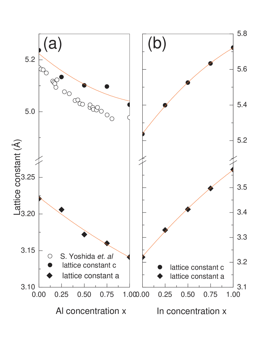
Table 1 summarizes our results and compares them with experimental and theoretical results reported previously using different methods. In going from GaN to AlN, when the Al–content increases, the values of the lattice parameters of the AlxGa1-xN alloy decrease. This is due to the fact that the size of the Al atom is smaller than the Ga atom. This is not the case for the internal parameter, , in which we observe an increase of this parameter when we increase the Al content of the alloy. Figure 1a depicts the behavior of the and parameters as a function of the Aluminum concentration. We can see from the figure that these parameters show a clear deviation from the linear behavior stated by Vegard’s law, which determines the parameter behavior of these alloys with a zinc–blende structure BTLiou . The deviation from Vegard’s law can be quantified by adjusting the curves in Figure 1a to the following formula:
| (1) |
where stands for the different structural parameters, and , of the AlxGa1-xN alloy. () represents the structural parameters of the binary AlN (GaN) compound and is the respective bowing parameter for the lattice and internal parameters. If we fit our calculated values from Table 1 to Eq. (1), we obtain a set of bowing parameters: Å, Å, and . We observe that all bowing parameters have a positive value, which indicates a downward bowing, being the lattice constant which possesses a larger deviation from the linear Vegard’s law, as was experimentally reported by S. Yoshida et al. SYoshida , and by Yun et al. FYun . Other works report that the lattice parameters follow Vegard’s law (see for example Angerer et al. HAngerer ); however, from from a theoretical approach, this alloy has only been studied using the virtual crystal approximation (VCA) by M. Goano et al. MGoano or by using first principles by Z. Dridi et al. ZDridi . Other authors have reported a non linear behavior of the lattice parameters, but their work demonstrates an upward bowing of the parameters Liou .
To compare our results with the available experimental information, we plot in Fig. 1a the calculated value of the parameter obtained by Eq. (1) together with the experimental results found in literature SYoshida . As we can see, our calculated values show the same trend depicted by the experimental data. Other examples of experimental studies for this alloy can be found in the works by D. K. Wickenden et al. DKWickenden , and by K. Itoh et al. KItoh .
III.1.2 InxGa1-xN
The recent developments in blue–green optoelectronics are essentially due to the high efficiency luminescence of InxGa1-xN/GaN heterostructures. Despite their importance, several properties of InxGa1-xN alloys are not fully understood. For example, the optical properties of InN crystals are poorly known since the available growth techniques have not allowed the production of high quality epitaxial layers. Recent improvements in the molecular beam epitaxy (MBE) technique have led to the availability of high quality InN films. Photoluminescence measurements of these films indicate an energy gap around 1 eV or less Davydov . The InxGa1-xN alloy has been studied theoretically by several groups using different methods. M. Goano et al. MGoano used pseudopotentials to compute the gap through the virtual crystal approximation approach. Z. Dridi et al. ZDridi used LDA FP–LAPW and the virtual crystal approximation approach. J. Serrano et al. JSerrano worked within the framework of the density functional theory (DFT) with the local density approximation (LDA) using the Ceperley–Alder form for the exchange– correlation energy. C. Stampfl et al. CStampfl utilized the DFT, the LDA, and the GGA of Perdew et al. for the exchange–correlation functional. A. Zoroddu et al. AZoroddu from first principles within the DFT utilized the plane–wave ultrasoft pseudopotential method within both the LDA and the GGA. And P. Carrier et al. PCarrier used plane–wave pseudopotentials and the LAPW method with the LDA.
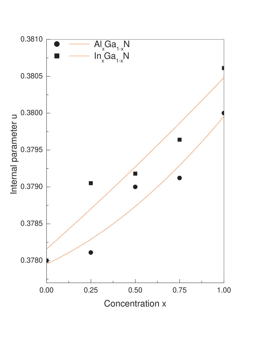
In Table 2 we summarize our results and compare them with some of the representative theoretical and experimental results found in literature. We can see from these results that the values of the and parameters increase when the In concentration increases. We plot these results in Fig. 1b. It is clear from the figure that, as in the previous case, there is not a linear dependence in these two parameters with an increase in the In concentration. If we adjust these results using Eq. (1), as we did for the AlxGa1-xN alloy, we obtain: Å, Å, and . For this alloy we can observe that the deviation parameters for both and have a negative value, which implies an upward bowing and is clearly observed in Fig. 1b. This is not the case for the internal parameter, , which has a nearly linear dependence with the In concentration as demonstrated by the bowing parameter, . The simulation results indicate that the lattice constant has a larger deviation from the linear Vegard’s law when compared with the lattice constant . Finally in Fig. 2, we plot the internal parameter, , for both alloys as a function of the concentration, . Solid circles and squares correspond to our theoretical results for AlxGa1-xN and InxGa1-xN, respectively, and the solid lines are obtained by fitting the results with Eq. (1).
After comparing our results with the experimental and theoretical works found in literature for both alloys we conclude that: 1) Our results for the binary compounds are in agreement with the published data, both experimental and theoretical. 2) For the AlxGa1-xN alloy, the structural parameters calculated in this work are in agreement with those reported in Ref. SYoshida . For this alloy, the bowing parameters for , have positive values, indicating a downward bowing. This is in agreement with experimental and theoretical results reported previously. 3) For the InxGa1-xN alloy, the bowing parameter of the lattice constants have a negative value, while the internal parameter, , has a positive value. Reported theoretical calculations do not give any information about the bowing for the parameter and it is not possible to obtain it from experimental measurements. To the best of our knowledge, this is the first time that the value of this parameter has been reported.
III.2 Electronic Structure for the AlxGa1-xN and InxGa1-xN alloys
Before presenting our results of the electronic structure, we provide a summary of some representative theoretical and experimental results reported in literature.
III.2.1 AlxGa1-xN
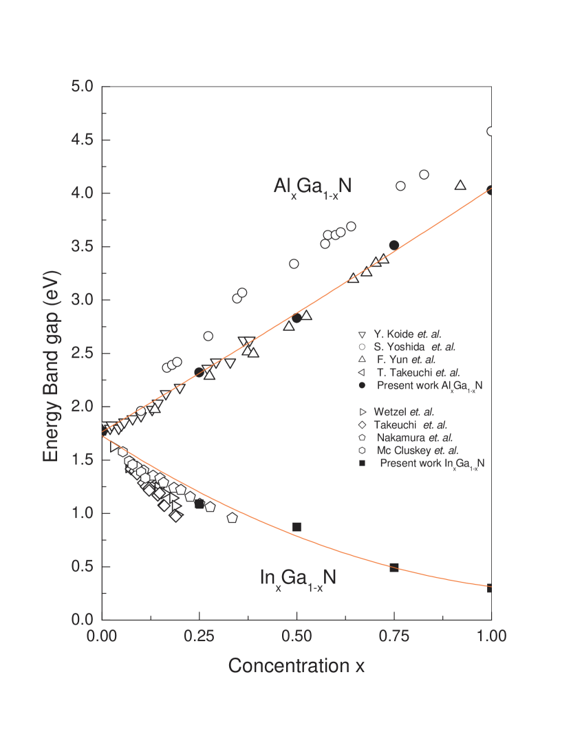
Hagan et al. JHagan and Baranov et al. BBaranov were the first to demonstrate experimentally the existence of the AlxGa1-xN alloy. Many other groups have measured its lattice constant, , the optical bowing parameter, , and the energy gap as a function of the concentration. The magnitude of the optical bowing parameter accounts for the deviation of the band gap from the linear dependence. Using MBE, S. Yoshida et al. SYoshida measured the lattice constant and the band gap for the entire interval of concentrations (). Comparing our results for the lattice constant with those reported by this author, there is a very good agreement over the entire interval of concentrations. Although our calculated band gap value shows the experimental trend reported by Yoshida et al. SYoshida , we obtain slightly different values as can be seen in Fig. 3. However, other reported values for the band gap are well reproduced in our calculations (see Fig. 3). There are many experimental reports for this system obtained by different techniques and for different values of the concentration. In all these references there is not a general agreement concerning if the fundamental parameters, i.e. the lattice constants and the band gap value, follow Vegard’s law. Positive, negative, or small values of the optical bowing parameter can be found throughout the literature YKoide ; SYoshida ; DKWickenden ; KItoh ; MAKhan ; THTakeuchi . Theoretical results have been reported using the kp method, the semi–empirical pseudopotentials method, ab initio LDA, DFT–LDA using molecular dynamics, and plane waves pseudopotentials using DFT–LDA.
III.2.2 InxGa1-xN
The first InxGa1-xN alloy with a high degree of ordering in layers grown on sapphire (0001) using metal–organic chemical vapor deposition (MOCVD) were obtained by Ruterana et al. PRuterana . Samples grown with different concentrations and using different techniques have been studied and authors report various values for the optical bowing parameter. In Table 3 we summarize the theoretical and experimental results obtained from the literature for both alloys along with our calculated values obtained for the optical bowing parameter. It can be seen from the table that there is a large discrepancy between the reported experimental and theoretical values. For theoretical calculations, most of the reported values are greater than one and they show a larger scattering of the numerical values, especially for the case of the InxGa1-xN alloy.
In Table 4 we show the obtained results for the energy gap of the AlxGa1-xN and InxGa1-xN alloys from our ab initio calculations for different values of the concentration, . These values correspond to % Al and In substitution, respectively. The plots corresponding to these data are displayed in Fig. 3. It can be seen that when the concentration of Al is increased the AlxGa1-xN alloy shows a nearly linear dependence. On the other hand, the InxGa1-xN alloy shows a non–linear dependence when we increase the In concentration. For both alloys we fit the gaps obtained by our calculations to a non–linear dependence using the quadratic phenomenological function:
| (2) |
where and Eg,B corresponds to the gap of the AlN (InN) and GaN for the AlxGa1-xN (InxGa1-xN) alloy. Substituting the values of Table 4 into Eq. (2) we found and 0.9990 for AlxGa1-xN and InxGa1-xN, respectively. The solid lines in Fig. 3 correspond to the non–linear fitting given by Eq. (2). It can be seen from this figure that there is a clear non–linear dependence for the InxGa1-xN alloy.
Concerning the electronic structure of these alloys, after comparing our results with those reported in literature we conclude that: 1) For both alloys, most of the experimental results consider concentrations lower than x=0.5. This could account for the scattered values reported for the bowing parameter; however, experiments considering the whole interval of concentrations are better reproduced by our calculations. 2) The obtained value in this work of for the bowing parameter of the AlxGa1-xN alloy is in agreement with most of the experimental and theoretical results reported previously. Although many authors claim that the dependence on concentration of the band gap parameter of this alloy should follow a Vegard’s–type law (), it has become more accepted that there is a small deviation in the linear dependence. 3) For the InxGa1-xN alloy the reported results show a large scattering, especially in the experimental data. This has been partially explained in the literature as due to an inaccurate determination of the concentration. The quality of the samples and the measurement technique also plays an important role in the determination of the optical bowing parameter. For this alloy, the scattering in the theoretical results reported in the literature is lower. Our calculations determined a value of , which is in good agreement with those reported previously.
Figure 3 shows a comparison of our theoretical results with the reported experimental results for the band gap energy as a function of concentration for the AlxGa1-xN and InxGa1-xN alloys. It can be seen from the figure that there is excellent agreement between our results and those reported, especially for the AlxGa1-xN alloy. Most of the reported results for the InxGa1-xN alloy are given for low concentrations of the In impurity. Nevertheless, our theoretical results follow the tendency demonstrated by experimental and theoretical results reported previously.
III.3 Calculated effective masses
As a by–product of our electronic band structure calculations, it is easy to compute the curvature of the minimum of the conduction band as well as the maximum of the valence band in the vicinity of the point. From these values the effective masses of the electrons and holes can be obtained.
At the point the like conduction band effective mass can be obtained through a simple parabolic fit using the definition of the effective mass as the second derivative of the energy band with respect to the wave vector, k, via:
| (3) |
where is the conduction electron effective mass and is the free electron mass.
The valence band states at the point are derived from bonding states and for the wurtzite crystals these states are not as symmetric as the conduction band. However, we can calculate the curvature of the valence band maximum using the following approach: if the spin–orbit interaction were neglected, the top of the valence band would have a parabolic behavior. This implies that the highest valence bands are parabolic in the vicinity of the point. In this work, all the systems studied satisfy this parabolic condition of the maximum of the valence band at the point Edmundo . Within this approach, and by using the appropriate expression of Eq. (3) (using a plus sign instead of the minus sign in the prefactor), we have calculated the effective masses of the heavy holes at the point.
Table 5 shows our calculated effective masses for the binary compounds, AlN, GaN, and InN, as well as for their related alloys. This table also includes theoretical and experimental values that were reported in literature, for comparison.
For the binary compounds, we conclude that our calculated effective masses are in the range of most of the reported theoretical and experimental values. Moreover, we obtain that our calculated values are in good agreement with the values recommended by Vurgaftman and Meyer IVurgaftman .
We report in the same table our calculated effective masses for the alloys studied in this work. The calculated value for the conduction electron effective mass for AlxGa1-xN increases as a function of the Al concentration. It should be noted that although we could not find published data for this parameter in the wurtzite phase, we did find calculated values for the electron effective mass of the alloy in the cubic phase RPaiva . The behavior for our calculations and the reported cubic phase values show the same trend. The same behavior was also obtained for the heavy hole effective mass.
The calculated effective masses for InxGa1-xN show a non monotonic behavior as a function of the In concentration as seen in Table 5. Comparison with empirical pseudopotential calculations for the conduction electron effective mass in the cubic phase of this alloy KKassali , reported for intermediate values of the In impurity, shows that we obtain similar behavior for our calculated effective masses.
III.4 Zone center phonon calculation
Using the frozen phonon approach, we can compute the zone center phonon modes, A and E, by considering the change of the total energy as a function of the displacement, , of the atoms in the unit cell from their equilibrium positions. In particular, we can compute the A mode by considering small displacements of the atoms along the optical axis (the c–axis) of the wurtzite phase. Then, as we are at the minimum of the total energy of the system, the perturbation around this minimum allows us to use the next parabolic approach to the total energy as a function of the displacement:
| (4) |
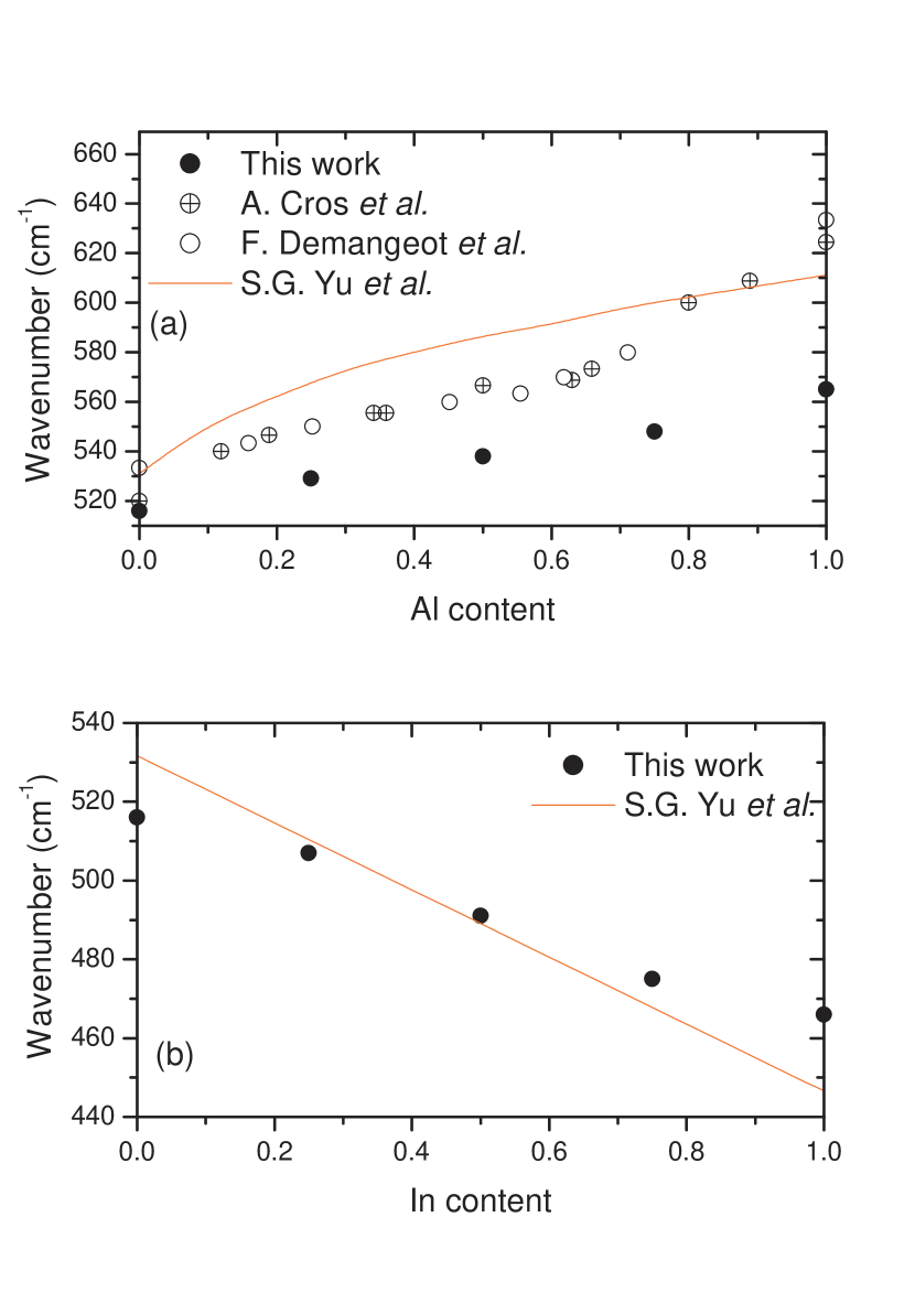
Where () are fit parameters, is the reduced mass, and is the frequency. With this approach, our calculated value for the mode for the binary compounds shows good agreement with most of the experimental reports as shown in Table 6. Figure 4a shows our calculated A mode for the AlxGa1-xN alloy, which is compared with the experimental data of Refs. ACros ; Demangeot , as well as the theoretical calculations of Ref. SGYu . Although, we obtain slightly different values over the range of Al concentration, we observe that the figure depicts the same trend shown by the experimental reports. Figure 4b shows our calculated A mode for the InxGa1-xN alloy and compares them with theoretical calculations reported in Ref. SGYu . As in the previous case, it can be seen that our calculated values for the A mode reproduce the trend reported in Ref. SGYu . In this way we show that our calculations properly reproduce the reported values of the A mode for the alloys and their binary parent compounds studied in this work.
IV Conclusions
We have calculated the structural and electronic properties of wurtzite AlN, GaN, InN, and their related alloys, AlxGa1-xN and InxGa1-xN. We found that, for both alloys, their structural parameters as a function of the concentration, , do not follow Vegard’s law. We observe that for the AlxGa1-xN alloy, the parameters have a positive bowing parameter, of which, the lattice constant, , demonstrates the largest value. On the other hand, when the concentration increases in the InxGa1-xN alloy, the bowing parameter for the and lattice constants have a negative value and the bowing parameter for the internal parameter, , remains positive. From our results of the electronic band structure calculations we obtained the band gap energy as a function of the concentration, , and characterized the deviation from the linear behavior by calculating the optical bowing parameter, . We obtain a small optical bowing parameter for the AlxGa1-xN alloy, which is consistent with results reported previously. The deviation from the linear behavior is more drastic for the InxGa1-xN alloy, which has in accordance with most of the experimental results found in literature. The effective masses of the systems studied in this work were calculated and we found that our calculated effective masses for the binary compounds, AlN, GaN, and InN, are in the range of the reported values in the recent literature. To the best of our knowledge, this is the first time that the deviation parameter for the internal parameter, , as well as the effective masses for these alloys have been reported. Finally, using the frozen phonon approach we have computed the A mode for the different systems studied in this work. From our calculations we have found good agreement with experimental values reported for the binary compounds. For the ternary alloys, our calculations reproduce experimental values for AlxGa1-xN, as well as theoretical predictions for InxGa1-xN.
Acknowledgements.
This work was done using the Computer Facilities of IPICYT, San Luis Potosí, México. This work was partially supported by VIEP–BUAP under grant VIEP–BUAP 1/I/EXC/05, VIEP–BUAP 01/EXC/06–I. ELA acknowledges to CONACyT under grat No.165404. This work was completed while DO was in a research stay at Freie Universität Berlin, the hospitality of H. Kleinert is greatly appreciated. DO gratefully acknowledges financial support from CINVESTAV–IPN and CONACYT–México.References
- (1) V. Yu. Davydov, A.A. Klochikhin, V.V. Emtsev, D.A. Kurdyukov, S.V. Ivanov, V.A. Vekshin, F. Bechstedt, J. Furthmüller, J. Aderhold, J. Graul, A.V. Mudryi, H. Harima, A. Hashimoto, A. Yamamoto, E.E. Haller, Phys. Status Solidi B, 234, 787 (2002).
- (2) Y. Koide, H. Itoh, M. R. H. Khan, K. Hiramatu, N. Sawaki, and I. Akasaki, J. Appl. Phys. 61, 4540 (1987).
- (3) H. Morkoç, S. Strite, G. B. Gao, M. E. Lin, B. Sverdlov, and M. Burns, J. Appl. Phys. 76, 1363 (1994).
- (4) J. I. Pankove, J. E. Berkeyheiser, H. P. Maruska and J. P. Wittke, J. Phys. Solid State Commun. 8, 1051, (1970).
- (5) J. I. Pankove, J. Lumin. 7, 114 (1973).
- (6) P. Hohenberg, W. Kohn, Phys. Rev. 136 864, (1964), Kohn, W., Sham, L. Phys. Rev. A 140 1133, (1965).
- (7) P. Blaha, K. Schwarz, G. K. H. Madsen, D. Kvasnicka, and J. Luitz, WIEN2K, An Augmented Plane Wave Plus Local Orbitals Program for Calculating Crystal Properties, ISBN 3–9501031–1–2, Vienna University of Technology, Austria, 2001.
- (8) J. P. Perdew and Y. Wang, Phys. Rev. B 45, 13244 (1992); J. P. Perdew, K. Burke, and M. Ernzerhof, Phys. Rev. Lett. 77, 3865 (1996).
- (9) H.J. Monkhorst and J.D. Pack, Phys. Rev. B 13, 5188 (1976).
- (10) B. T. Liou, Appl. Phys. A, 86, 539 (2007).
- (11) M. Goano, E. Bellotti, E. Ghillino, G. Ghione, and K. F. Brennan, J. Appl. Phys. 88, 6476 (2000).
- (12) Z. Dridi, B. Bouhafs, and P. Ruterana, Phys. Stat. Sol. (c), 0, 315, (2002); Z. Dridi, B. Bouhafs, and P. Ruterana, Semicond. Sci. and Technol. 18, 850 (2003).
- (13) S. Yoshida, S. Misawa, and S. Gonda, J. Appl Phys. 53, 6844, (1982).
- (14) F. Yun, M. A. Reshchikov, L. He, T. King, H. Morkoç, S. W. Novak and L. Wei, J. Appl. Phys. 92, 4837 (2002).
- (15) H. Angerer, App. Phys. Lett. 71, 1504 (1997).
- (16) B. T. Liou, Appl. Phys. A 81, 1459 (2005).
- (17) D. K. Wickenden, C. B. Bargeron, W. A. Bryden, J. Miragliotta, and T. J. Kistenmacher, Appl. Phys. Lett.65, 2024 (1994).
- (18) K. Itoh, T. Kawamoto, H. Amano, K. Hiramatsu and I. Akasaki, Jpn. J. Appl. Phys. 30, 1924 (1991).
- (19) S. Strite and H. Morkoç, J. Vac. Sci. Technol. B 10, 1237 (1992), and references therein.
- (20) T. Detchprohm, K. Hiramatsu, K. Itoh, and I. Akasaki, Jpn. J. Appl. Phys. Part 2 31, L1454 (1992).
- (21) M. Leszczynski, T. Suski, H. Teisseyre, P. Perlin, I. Grzegory, J. Jun, S. Porowski, and T. D. Moustakas, J. Appl. Phys. 76, 4909 (1994).
- (22) H. Schulz and K. H. Thiemann, Solid State Commun. 23, 815 (1977).
- (23) M. Tanaka, S. Nakahata, K. Sogabe, H. Nakata and M. Tobioka, Jpn. J. Appl. Phys. 36, L1062 (1997).
- (24) A. F. Wright and J. S. Nelson, Phys. Rev. B 51, 7866 (1995).
- (25) C. Bungaro, K. Rapcewicz, and J. Bernholc, Phys. Rev. B 61, 6720 (2000).
- (26) J. Serrano and A. Rubio, Phys. Rev. B 62, 16612 (2000).
- (27) C. Stampfl, C. G. Van de Walle, Phys. Rev. B 59, 5521 (1999).
- (28) A. Zoroddu, F. Bernardini, P. Ruggerone and V. Fiorentini, Phys. Rev. B 64, 045208 (2001).
- (29) P. Carrier and S. Wei, J. Appl. Phys. 97, 033707 (2005).
- (30) W. Paszkowicz, Powder Diffr. 14, 258 (1999).
- (31) T. L. Tansley and C. P. Foley, J. Appl. Phys. 59, 3241 (1986).
- (32) K. Kubota, Y. Kobayashi and K. Fujimoto, J. Appl. Phys. 66, 2984 (1989).
- (33) J. Hagan, R. D. Metcalfe, D.Wickenden, and W. Clark, J. Phys. C 11, L143 (1978).
- (34) B. Baranov, L. Daweritz, V. B. Guton, G. Jungk, H. Neumann, and H. Raidt, Phys. Status Solidi A 49, G29 (1978).
- (35) M. A. Khan, R. A. Skogman, R. G. Schulze and M. Gershenzon, Appl. Phys. Lett. 43, 492, (1983).
- (36) T. Takeuchi, H. Takeuchi, S. Sota, H. Sakai, H. Amano and I. Akasaki, Jpn. J. Appl. Phys. 36, L177 (1997).
- (37) K. Chen and D. A. Drabold, J. Appl. Phys. 91, 9743 (2002).
- (38) S. K. Pugh, D. J. Dugdale, S. Brand and R. A. Abram, J. Appl. Phys. 86, 3768 (1999).
- (39) O. Ambacher, J. Phys. D: Appl. Phys. 31, 2653 (1998).
- (40) S. Nakamura, J. Vac. Sci. Technol. A 13, 705 (1995).
- (41) M. D. McCluskey, C. G. Van de Walle, C. P. Master, L. T. Romano, and N. M. Johnson, Appl. Phys. Lett. 72, 2725 (1998).
- (42) C. Wetzel, T. Takeuchi, S. Yamaguchi, H. Katoh, H. Amano, and I. Akasaki, Appl. Phys. Lett. 73, 1994 (1998).
- (43) C. Caetano, L. K. Teles, M. Marques, A. Dal Pino, Jr., and L. G. Ferreira, Phys. Rev. B 74, 045215 (2006).
- (44) J. Wu, W. Walukiewicz, K. M. Yu, J. W. Ager III, E. E. Haller, H. Lu, W. J. Schaff, Phys. Stat. Sol. (b) 240, 412 (2003).
- (45) P. Ruterana, G. Nouet, W. Van der Stricht, I. Moerman and L. Considine, Appl. Physc. Lett. 72, 1743 (1988).
- (46) See Figures 5.11–5.20 in E. López–Apreza, Ph. D. Thesis, BUAP, Puebla, Mexico (http://www.fis.cinvestav.mx/~daniel/thELA.pdf)
- (47) R. de Paiva, J.L.A. Alves, R.A. Nogueira, C. de Oliveira, H.W.L. Alves, L.M.R. Scolfaro, nd J.R. Leite, Mat. Scie. and Enginnering B 93, 2, (2002).
- (48) K. Kassali and N. Bouarissa, Solid–State Electronics, 44 501, (2000).
- (49) I. Vurgaftman and J. R. Meyer, J. Appl. Phys. 94, 3675 (2003).
- (50) P. Perlin, E. Litwin–Staszewska, B. Suchanek, T. Suski, R. Piotrzkowski, I. Grzegory, S. Porowski, E. Kaminska, Appl. Phys. Lett. 68, 1114 (1996)
- (51) Y. J. Wang, R. Kaplan, H. K. Ng, K. Doverspike, D. K. Gaskill, T. Ikedo, I. Akasaki, and H. Amono, J. Appl. Phys. 79, 8007 (1996)
- (52) J. S. Im, A. Moritz, F. Steuber, V. Härle, F. Scholz, and A. Hangleiter, Appl. Phys. Lett. 70, 631 (1997)
- (53) S. K. O’Leary, B. E. Foutz, M. S. Shur, U. V. Bhapkar, L. F. Eastman, J. Appl. Phys. 83, 826 (1998)
- (54) S. Elhamri, R. S. Newrock, D. B. Mast, M. Ahoujja and W. C. Mitchel, Phys. Rev. B 57, 1374 (1998)
- (55) Y. C. Yeo, T. C. Chong, and M. F. Li, J. Appl. Phys. 83, 1429 (1998)
- (56) J. D. Albrecht, R. P. Wang, P. P. Ruden, M. Farahmand and K. F. Brennan, J. Appl. Phys. 83, 1446 (1998)
- (57) Brian E. Foutza, Stephen K. O’Leary, Michael S. Shur, and Lester F. Eastman J. Appl. Phys. 85, 7728 (1999)
- (58) P. Rinke, M. Winkelnkemper, A. Qteish, D. Bimberg, J. Neugebauer, and M. Scheffler, Phys. Rev. B 77, 075202 (2008).
- (59) A. Cros, H. Angerer, 0. Ambacher, M. Stutzmann, R. Hopler, and T. Metzge, Solid State Comm. 104, 35 (1997).
- (60) F. Demangeot, J. Groenen, J. Frandon, M. A. Renucci, O. Briot, S. Clur, and R. L. Aulombard, J. Appl. Phys. 72, 2674 (1998).
- (61) SeGi Yu, K. W. Kim, and L. Bergman, Phys. Rev. B 58, 15283 (1998).
- (62) T. Y. Lin, H. M. Chen, M. S. Tsai, Y. F. Chen, F. F. Fang, C. F. Lin and G. C. Chi Phys. Rev. B 58 13793 (1998).
- (63) A. Saxler, P. Debray, R. Perrin, S. Elhamri, W. C. Mitchel, C. R. Elsass, I. P. Smorchkova, B. Heying, E. Haus, P. Fini, J. P. Ibbetson, S. Keller, P. M. Petro, S. P. DenBaars, U. K. Mishra, and J. S. Speck J. Appl. Phys. 87, 369 (2000).
- (64) D. Fritsch, H. Schmidt, and M. Grundmann, Phys. Rev. B 69, 165204 (2004).
- (65) I. Gorczyca, N. E. Christensen, E. L. Peltzer y Blanc, and C. O. Rodríguez, Phys. Rev. B 51, 11936 (1995).
- (66) M. R. Aouas, W. Sekkal, A. Zaoui Solid State Comm. 120, 413 (2001).
- (67) V. Yu. Davydov, Yu. E. Kitaev, I. N. Goncharuk, A. N. Smirnov, J. Graul, O. Semchinova, D. Umann, M. B. Smirnov and A. P. Mirgorodsky, R. A. Evarestov Phys Rev. B 58, 12899 (1998).
- (68) J. M. Zhang, T. Ruf, M. Cardona, O. Ambacher, M. Stutzmann, J. M. Wagner and F. Bechstedt Phys Rev. B 56, 14399 (1997).
- (69) K. Karch and F. Bechstedt Phys Rev. B 56, 7404 (1997).
- (70) G. Kaczmarczyk, A. Kaschner, S. Reich, A. Homann, C. Thomsen, D. J. As, A. P. Lima, D. Schikora, K. Lischka, R. Averbeck and H. Riechert Appl. Phys Lett. 76, 2122 (2000).
- (71) V. Yu. Davydov, V. V. Emtsev, I. N. Goncharuk, A. N. Smirnov, V. D. Petrikov, V. V. Mamutin, V. A. Vekshin, S. V. Ivanov, M. B. Smirnov, T. Inushima Appl. Phys. Lett. 75, 3297 (1999).
- (72) Due to the band-gap problem in ab initio calculations and, in order to show a better comparison with our calculations, we have rigidly moved downward the experimental data without lost of validity.
| Present Work | Exp. Results | Other Calc. | ||
| GaN | a | 3.2209 | 3.1890111Ref. SStrite , 3.1892222Ref. TDetchprohm | 3.1660333Ref. ZDridi , 3.189444Ref. AFWright , 3.2555Ref. CBungaro |
| 3.1880666Ref. MLeszczynski , 3.19777Ref. HSchulz | 3.1800888Ref. JSerrano , 3.1986999Ref. AZoroddu , 3.17101010Ref. PCarrier , 3.183111111Ref. Liou | |||
| c | 5.2368 | 5.1850a, 5.185b | 5.1540c, 5.185d, 5.2200e | |
| 5.18561f, 5.189g | 5.1898h, 5.2262i 5.151j, 5.178k | |||
| u | 0.3780 | 0.3768a, 0.377g | 0.3770c, 0.3768d, 0.3760e | |
| 0.3760h, 0.3772i, 0.3768j | ||||
| Al0.25Ga0.75N | a | 3.2059 | See Ref. SYoshida ; FYun | 3.163k |
| c | 5.1338 | 5.137k | ||
| u | 0.3781 | |||
| Al0.50Ga0.50N | a | 3.1719 | See Ref. SYoshida ; FYun | 3.139k |
| c | 5.1012 | 5.085k | ||
| u | 0.3790 | |||
| Al0.75Ga0.25N | a | 3.1601 | 3.098k | |
| c | 5.0870 | See Ref. SYoshida ; FYun | 4.990k | |
| u | 0.3791 | |||
| AlN | a | 3.1411 | 3.1120a, 3.11g | 3.0920c, 3.084d, 3.1e |
| 3.1106121212Ref. MTanaka | 3.0610h, 3.10954i, 3.098j, 3.076k | |||
| c | 5.0268 | 4.9820a, 4.98g | 4.954c, 4.9948d, 5.010e | |
| 4.9795l | 4.8976h, 4.9939i, 4.9599j, 4.935k | |||
| u | 0.3805 | 0.3819a, 0.3821g | 0.3821c, 0.3814d, 0.3800e | |
| 0.3820h, 0.3819i, 0.3819j |
| Present Work | Exp. Results | Other Calc. | ||
| GaN | a | 3.2209 | 3.1890131313Ref. SStrite , 3.1892141414Ref. TDetchprohm | 3.1660151515Ref. ZDridi , 3.189161616Ref. AFWright , 3.2000171717Ref. CBungaro |
| 3.1880181818Ref. MLeszczynski , 3.19191919Ref. HSchulz | 3.1800202020Ref. JSerrano , 3.1986212121Ref. AZoroddu , 3.17222222Ref. PCarrier | |||
| c | 5.2368 | 5.1850a, 5.185b | 5.1540c, 5.185d, 5.2200e | |
| 5.18561f, 5.189g | 5.1898h, 5.2262i, 5.151j | |||
| u | 0.3780 | 0.3768a, 0.377g | 0.3770c, 0.3768d, 0.3760e | |
| 0.3760h, 0.3772i, 0.3768j | ||||
| In0.25Ga0.75N | a | 3.3298 | ||
| c | 5.3987 | |||
| u | 0.3791 | |||
| In0.50Ga0.50N | a | 3.4128 | ||
| c | 5.5257 | |||
| u | 0.3792 | |||
| In0.75Ga0.25N | a | 3.4969 | ||
| c | 5.6333 | |||
| u | 0.3796 | |||
| InN | a | 3.5440 | 3.5365232323Ref. Davydov , 3.5378242424Ref. Paszkowicz | 3.520c, 3.501d, 3.480e |
| 3.548252525Ref. Tansley , 3.540262626Ref. Kubota | 3.525h, 3.614i, 3.546j | |||
| c | 5.7228 | 5.7039k, 5.7033l | 5.675c, 5.669d, 5.64e | |
| 5.76m, 5.705n | 5.68583h, 5.8836i, 5.7162j | |||
| u | 0.3806 | 0.3799c, 0.3784d, 0.378e | ||
| 0.379h, 0.37929i, 0.379j |
| AlxGa1-xN | |||
| Experimental | [eV] | Theoretical | [eV] |
| YKoide Y. Koide, for using MOVPE | MGoano M. Goano using pseudopotentials and VCA | 0.069 | |
| SYoshida S. Yoshida, using MBE at | ZDridi Z. Dridi using FP–LAPW LDA and VCA | 0.710 | |
| FYun F. Yun, for using MBE at | 1 | DKWickenden D. K. Wickenden, using MOCVD | |
| MAKhan M. A. Khan, using MOCVD at | KChen K. Chen using ab initio Molecular dynamics | 1.40 | |
| THTakeuchi T. Takeuchi, for using MOVPE | SKPugh S. K. Pugh using first principles method | ||
| OAmbacher O. Ambacher Review article | 1 | Value calculated in this work | 0.3185 |
| InxGa1-xN | |||
| Experimental | [eV] | Theoretical | [eV] |
| Davydov V. Yu. Davydov et al. for | 2.50 | MGoano M. Goano et al. | 1.05 |
| THTakeuchi T. Takeuchi et al. | 3.20 | ZDridi Z. Dridi et al. | 1.70 |
| SNakamura S. Nakamura et al., for | 1.00 | CCaetano C. Caetano et al., using FP and LDA | 1.44 |
| MDMcCluskey M. D. McCluskey et al., for | 3.5 | AFWright A. F. Wright et al. | 0.1677 |
| CWetzel C. Wetzel et al., for using MOVPE | 2.6 | Value calculated in this work | 0.999 |
| JWu J. Wu et al., for using MBE | 1.4 |
| System | Egap(eV) |
|---|---|
| GaN | 1.768 |
| Al0.25Ga0.75N | 2.319 |
| Al0.50Ga0.50N | 2.830 |
| Al0.75Ga0.25N | 3.5123 |
| AlN | 4.027 |
| GaN | 1.768 |
| In0.25Ga0.75N | 1.088 |
| In0.50Ga0.50N | 0.871 |
| In0.75Ga0.25N | 0.489 |
| InN | 0.299 |
| Present work | Other results | ||||||
| AlN | 0.3012 | 4.3243 | 0.30272727Ref. IVurgaftman | 0.33282828Ref. Rinke | 0.33292929Ref. PCarrier | 4.35c | |
| 0.2847 | 0.2427 | 0.32a | 0.32b | 0.32c | 0.28c | ||
| 0.2956 | 1.6528 | 0.31303030Ref. JDAlbrect | 0.48313131Ref. BEFoutza | ||||
| Al0.75Ga0.25N | 0.2682 | 3.5247 | |||||
| 0.2913 | 0.9325 | ||||||
| 0.2749 | 1.4743 | ||||||
| Al0.50Ga0.50N | 0.2330 | 2.3039 | |||||
| 0.2411 | 0.5345 | ||||||
| 0.2427 | 1.2961 | ||||||
| Al0.25Ga0.75N | 0.2020 | 3.1232 | |||||
| 0.1958 | 0.1741 | ||||||
| 0.2000 | 1.1969 | ||||||
| GaN | 0.1491 | 2.1072 | 0.20a | 0.21b | 0.22c | 0.39c | |
| 0.1803 | 2.1048 | 0.20a | 0.19b | 0.20c | 2.04c | ||
| 0.1692 | 2.1412 | 0.22323232Ref. PPerlin | 0.23333333Ref. YJWang | 0.20343434Ref. SKOLeary | 2.2353535Ref. JSIm | ||
| 0.18363636Ref. SElhamri | 0.20373737Ref. BEFoutza | 0.24383838Ref. TYLim | |||||
| 0.215393939Ref. ASaxler | |||||||
| In0.25Ga0.75N | 0.1069 | 2.5409 | |||||
| 0.0968 | 2.4447 | ||||||
| 0.1035 | 2.4953 | ||||||
| In0.50Ga0.50N | 0.1182 | 2.7958 | |||||
| 0.0921 | 2.6116 | ||||||
| 0.1025 | 2.8371 | ||||||
| In0.75Ga0.25N | 0.0717 | 2.0304 | |||||
| 0.0623 | 2.1486 | ||||||
| 0.0781 | 2.2179 | ||||||
| InN | 0.1299 | 1.9096 | 0.07a | 0.068b | 0.07c | 2.967404040Ref. Fritsch | |
| 0.068n | |||||||
| 0.0892 | 2.2051 | 0.07a | 0.065b | 0.06c | 2.566n | ||
| 0.072n | |||||||
| 0.1146 | 2.0301 | ||||||
| System | Present work | Other results | Experimental | ||||
|---|---|---|---|---|---|---|---|
| GaN | 516 | 537414141Ref. Gorczyca | 545424242Ref. Aouas | 533.8434343Ref. YuDavidov | 533.5444444Ref. Zhang | ||
| Al25Ga75N | 529 | ||||||
| Al50Ga50N | 538 | ||||||
| Al25Ga25N | 548 | ||||||
| AlN | 565 | 649a | 615c | 619454545Ref. Karch | 613.8c | ||
| In25Ga75N | 507 | ||||||
| In50Ga50N | 491 | ||||||
| In75Ga25N | 475 | ||||||
| InN | 466 | 443464646Ref. Kaczmarczyk | 447474747Ref. YuDavidov2 | 440f | |||