Optical orientation in bipolar spintronic devices
Abstract
Optical orientation is a highly efficient tool for the generation of nonequilibrium spin polarization in semiconductors. Combined with spin-polarized transport it offers new functionalities for conventional electronic devices, such as pn junction bipolar diodes or transistors. In nominally nonmagnetic junctions optical orientation can provide a source for spin capacitance—the bias-dependent nonequilibrium spin accumulation—or for spin-polarized current in bipolar spin-polarized solar cells. In magnetic junctions, the nonequilibrium spin polarization generated by spin orientation in a proximity of an equilibrium magnetization gives rise to the spin-voltaic effect (a realization of the Silsbee-Johnson coupling), enabling efficient control of electrical properties such as the I-V characteristics of the junctions by magnetic and optical fields. This article reviews the main results of investigations of spin-polarized and magnetic pn junctions, from spin capacitance to the spin-voltaic effect.
I Introduction
Semiconductor spintronics Fabian et al. (2007); Žutić et al. (2004) has inspired fascinating developments in spin-based electronics as well as in our understanding of fundamental spin-related processes in solids. In particular, we have learned how to control spin by electric and optical means, and how the presence of spin is manifested in electronic and optical Meier and Zakharchenya (1984) (Eds.) processes. This article discusses selected device schemes inspired by optical orientation of nonequilibrium spin, as well as by the fundamental concept of spin-charge coupling, originally proposed by Silsbee and Johnson for metals. Silsbee (1980); Johnson and Silsbee (1985)
The device settings we consider are spin-polarized pn junctions and magnetic diodes, forming building blocks of bipolar spintronics. While we review the most important results and present selected functionalities of the devices, we first briefly comment on the methodology we use to study them. Our proposals are based on two approaches: (i) fully numerical self-consistent calculations of the spin-polarized drift-diffusion transport and (ii) analytical modeling in the regime of low injection.
The main idea behind the numerical approach is designing a discretization scheme to solve a set of coupled differential equations for drift-diffusion transport. We typically consider electrons as spin-polarized, leaving holes unpolarized. This is justified by the fast spin relaxation of holes in zinc-blend semiconductors which could be used as the materials of choice in bipolar spintronic devices (silicon alone is ineffective as far as optical orientation is concerned). While there is no technical difficulty of involving spin-polarized holes, the presentation is focused on the most important effects when considering only electrons as the carriers of spin.
Let us denote by the electron diffusion coefficient, by and the electron and electron spin densities, by the electrostatic potential inside the device (consisting of the equilibrium built-in field as well as the field coming from the external emf source; the label stands for total), and by the spin-splitting, in general spatially varying, of the conduction band. The drift-diffusion prescription for the electron particle and electron spin currents is
| (1) | |||||
| (2) |
We express the energy ( and ) in the units of thermal energy, . We also assume the semiconductors are nondegenerate, with all the donors/acceptors fully polarized. In fact, for the numerical illustrations we consider room temperature (and give bias in volts). A similar expression as for can be written for the hole current, , for holes in the valence band.
Electrons and holes are coupled by the recombination processes. Since we consider optically active zinc-blende materials, the presumed coupling is through the electron-hole recombination, of the rate coefficient , described by the following continuity equations:
| (3) | |||||
| (4) |
The hole density is and the equilibrium densities (at absent bias and optical generation) are indexed with zero. The continuity equation for spin takes into account that the spin density decays by both the electron-hole recombination as well as by intrinsic spin relaxation, of the rate of the inverse of the spin relaxation time . Important, is the deviation of the instantaneous spin density from the spin density that would be the equilibrium one for the instantaneous electron density: , where is the equilibrium spin polarization. The spin decays to , not to , as reflects intrinsic spin relaxation processes Meier and Zakharchenya (1984) (Eds.); electron-hole recombination, which also degrades spin, is considered explicitly. Optical generation of charges or spin can be described according to the specific situation, either through boundary conditions on the nonequilibrium spin or charge, if the light is incident through the edges, or through the constant photoexcitation rates for electrons and for the spin. In zinc-blend semiconductors , since the spin polarization of electrons at the time of pair creation is . Meier and Zakharchenya (1984) (Eds.) In addition to the external spin sources due to spin injection or optical orientation, there will be spin polarization in our bipolar system due to spin-orbit coupling. Such intrinsic spin polarizations will be typically much smaller (say, on the order of 0.1%) than those considered here. Tse et al. (2005).
Finally, the self-consistent loop is completed by coupling the transport to the local charge density via the Poisson equation,
| (5) |
with collecting all the contributions (generally, spatially dependent) consisting of ionized donors (), acceptors (), and the electron () and hole () densities:
| (6) |
We stress that the effects of the electric field are included by default in this scheme.
While the numerical approach is essential in modeling general transport conditions, at low injections (small biases—typically applied voltages smaller than the energy band gap of the host material) the numerical simulations can be remarkably well substituted by a few assumptions allowing for rather simple analytical modeling. Following the original insight of Shockley Shockley (1950), who has pioneered the low injection transport modeling of bipolar devices, we have formulated the assumption governing spin-polarized drift diffusion in generic devices containing spin sources as well as the spin splitting of the carrier energy bands. Fabian et al. (2002a) The conditions, valid in the low injection limit, are: (a) the bulk regions (those away from the depletion layers) are neutral, (b) there is a thermal quasiequilibrium across the depletion layer at applied biases and at the presence of source spin (this essentially means that spin-resolved chemical potentials are constant across the depletion layer), and (c) the spin current is continuous across the depletion layer. The last condition can be relaxed and substituted by a current continuity model of spin relaxation in the depletion layer.
The analytical theory and its ramifications for spin-polarized bipolar transport is worked out in Ref. Fabian et al., 2002a. Here we list the most important conclusions, which follow from the generalized Shockley conditions a) and b) above. First, there is a nice relation connecting the spin density polarizations,
| (7) |
across the depletion layer. If the p region is on the left () of the layer, and the n region on the right (), the relation can be stated as,
| (8) |
The zero-indexed polarizations are the equilibrium ones. In addition,
| (9) |
denotes the nonequilibrium part of the polarization. We will find this equation useful in discussing the physics of spin injection across the depletion layer in spin-polarized pn junctions.
There are also relations connecting the carrier and spin densities across the depletion layer. We have,
| (10) | |||||
| (11) |
recall that the applied bias is measured in the units of thermal energy . For spin-unpolarized case, , the voltage dependence of , the electron density in the p region close to the depletion layer follows the typical rectification behavior (actually giving rise to the rectification I-V characteristic); is small for reverse biases (), while it exponentially increases for forward biases () with increasing . In the spin-polarized case the electron density and the resulting electron current are modified by , the amount of nonequilibrium spin in the n region, but only if there is an equilibrium spin polarization present. This is the statement of the spin-charge coupling, applied to pn junctions. Compared to metal physics, the coupling is actually exponentially amplified by the applied forward bias, leading to a strong giant-magnetoresistance like behavior of magnetic pn junction diodes, as will be discussed later.
The relations Eqs. 8 and 10 contain an unknown parameter, . Typically we set our boundary conditions far from the depletion layer, simulating carrier and spin injection. The nonequilibrium spin at the depletion layer is a result of a self-consistent spin distribution throughout the junction, and to obtain it the last condition, c), needs to be invoked. The result is an analytical formula for which allows fully analytical modeling of the spin injection physics. Fabian et al. (2002a) We do not reproduce this formula here.
In addition to the usual definition of spin polarization, given in Eq. 7, we also introduce the spin polarization of the electric current,
| (12) |
as the ratio of the spin and (total) charge current. Since unlike the charge current the spin current is not conserved (and is in general not uniform throughout the space), the spin current polarization is typically space dependent. Normally we are concerned about the current spin polarization at the contacts with electrodes, as the spin injection efficiency is directly proportional to it; see the discussion of spin injection in Refs. Žutić et al., 2004 and Fabian et al., 2007.
Other bipolar devices, not discussed here, include spin light-emitting Fiederling et al. (1999, 2003); Ohno et al. (1999); Young et al. (2002); Jonker et al. (2000); Hanbicki et al. (2002); Jiang et al. (2003); Zega et al. (2006) and, in some sense, spin Esaki diodes. Kohda et al. (2001); Johnston-Halperin et al. (2002) We also list alternative spintronic device schemes that may be practical in the long run: resonant tunneling diodes Ertler and Fabian (2006a, b); Ertler and Fabian (2007); Slobodskyy et al. (2003); Petukhov et al. (2002); Ertler and Fabian (2008), a room temperature spin-transference device Dery et al. (2006a) or a scheme for reconfigurable logic Dery et al. (2007) , unipolar magnetic diodes Flatté and Vignale (2001), to name a few.
Optical orientation can also be useful to detect spin in otherwise optically inactive materials (such as silicon), by surrounding the material with an optically active material (such as GaAs) and allow for spin transfer. Such a scheme was proposed to detect spin injection into silicon Žutić et al. (2006), as a recently experimentally demonstrated Jonker et al. (2007); van ’t Erve et al. (2007) alternative way to an all-electron detection Appelbaum et al. (2007); Huang et al. (2007); Žutić and Fabian (2007) in this prominent material.
Yet other important applications of optical spin orientation are spin-polarized bipolar semiconductor lasers. It was demonstrated that pumping a vertical-cavity surface emitting laser (VCSEL) with optically generated spin-polarized carriers can lead to the lasing operation at the reduced threshold current as compared to the spin-unpolarized VCSEL. Rudolph et al. (2003, 2005) For a fixed pump power, the emitted power of the laser can be increased by 400 % by simply changing the degree of spin polarization of pumped carriers. Rudolph et al. (2003) Both the threshold current reduction and the change of emitted power with the variation of spin polarization of pumped carriers have also been demonstrated in electrically pumped VCSEL. Holub et al. (2007); Holub and Bhattacharya (2007) It was recently shown Gothgen et al. (2008) that spin VCSELs could exceed previously accepted theoretical limit (50 %) for the threshold reduction and act as efficient nonlinear filters of circularly-polarized light. While the work on spin VCSELs has emerged only in the last several years, it already shows a clear path towards practical realization. Revealing novel effects in semiconductor spin lasers will closely depend on our ability to better understand the interplay of optical orientation and bipolar transport.
II Spin-polarized pn junctions: spin capacitance
When nonequilibrium spin is injected in nominally nonmagnetic pn junctions, we speak of spin-polarized pn junctions. The spin injection can be done optically or electrically and, while the specifics of the device depends on the injection mode—through specific boundary conditions for the current or carrier concentrations—for the principle of operation it does not matter. In what follows we consider optical orientation which gives both nonequilibrium spins and charges at the spin injection point; in the case of an electrical spin injection carriers would be at thermal equilibrium, in ohmic contacts.
The pn junction has three regions: p-region, n-region, and the depletion layer in between. The operation of the junction depends on in which region the nonequilibrium or source spin is injected. In the following we consider only electrons as spin polarized; holes are kept unpolarized. This is partly justified by the fact that holes in bulk zinc-blende semiconductors lose spin polarization very fast, on the order of the momentum relaxation time. If the spin is injected into the p-region, the minority carrier (electrons) are spin polarized, carrying the spin polarization through the depletion layer into the n-region. The consequences are spin pumping as well as the spin capacitance effect, as discussed below. If the spin is injected into the depletion layer, or in a close proximity, the pn junction functions as a spin-polarized solar cell, the subject of the following section. Finally, if the spin is injected into the n-region, orienting the majority carriers, ordinary spin injection into the p-region follows under forward bias.
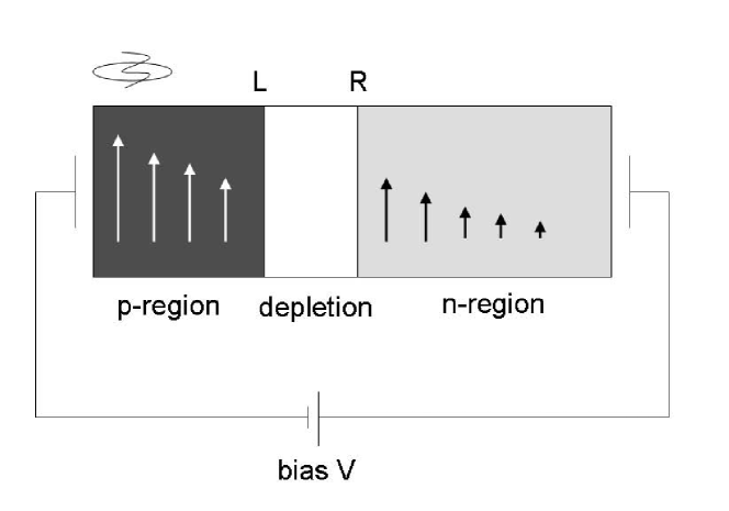
Suppose a nonequilibrium spin is injected into the p-region, as illustrated in Fig. 1. The spin propagates by drift-diffusion towards the depletion layer. Assuming the spin injection point is within the spin diffusion length from the depletion layer, a significant spin polarization survives there. What happens to the spin in the depletion layer? The large built-in field (typically tens of kV/cm) sweeps all the electrons to the n-region. Since the spin is attached to the carriers, the spin density follows. In the n-region the spin accumulates, creating a spin density gradient and setting up a back-diffusion. In the steady state process the spin influx balances the back-diffusion. We termed this process spin pumping by the minority channel. Žutić et al. (2001a) Interestingly, the injected spin density is (spatially) amplified as it goes through the depletion layer. On the other hand, the spin polarization is preserved, at least at low biases; it is not amplified. This follows from a general result, that the nonequilibrium spin polarizations at the p-side ( for the left) and at the n-side ( for the right) of the depletion layer of a nonmagnetic pn junction are the same, in the low injection limit (see Eq. 8):
| (13) |
as for nonmagnetic junctions. The argument, based on generalized Shockley’s conditions, is presented in Ref. Fabian et al., 2002a.
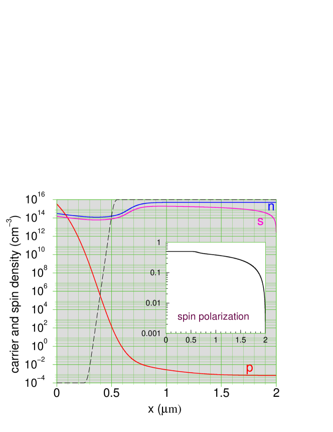
In Fig. 2 we plot the results of a self-consistent drift-diffusion calculation for a GaAs inspired nondegenerate pn junction with optical spin injection (source spin) in the p region. As optically both spin and electron-hole pairs are created, the electron density in the p-region is also enhanced. The spin density decays somewhat towards the depletion layer, essentially following the decrease of the nonequilibrium electron density due to electron-hole recombination processes. Both densities are strongly enhanced in the n region, although the spin polarization itself stays unchanged, disappearing at the far edge of the n region only. The figure demonstrates both the spin pumping through the minority channel as well as the spin density amplification.
If we look at the spin polarization, plotted in Fig. 3 we see at first a surprising decrease of its magnitude with increasing the bias voltage. Recall that a negative bias results in a reverse regime, at which only very little (so called generation) current flows through the junction. In this regime the depletion layer widens and the built-in electric field increases. The intrinsic barrier for the carriers to cross from one region to the other increases, inhibiting the current flow. For the spin injection the reverse region means that the minority electrons have reduced distances to go to the wider depletion layer (the spin injection point is fixed), so that the electrons have less time to recombine with holes and large electron and the accompanying spin densities arrive at the boundary of the depletion layer. These electrons are then swept by the increased built-in field into the n region, pumping the spin there.
If the source spin is added to the n region, under forward biases the spin can be injected into the p region. See Fig. 3. The spin injection process is straightforward: spin is injected along with the nonequilibrium electron density into the p region, in which both the spin and the carrier density decay mainly by electron-hole recombination. In the reverse bias the spin injection is severely inhibited.
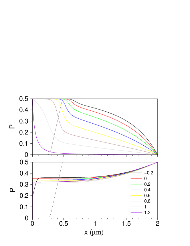
Spin-polarized pn junctions exhibit the spin capacitance phenomenon. Following an analogy with conventional charge capacitance we define the spin capacitance as the change of the nonequilibrium spin due to an increment of bias voltage. The accumulated spin in the junction is maintained both by the source spin and by the bias voltage. If the source spin is turned off, no spin accumulation is present. The bias voltage is an additional spin control knob. We consider the case of the source spin in the p region. As the bias voltage is increased from reverse to forward, the total accumulated spin in the pn junction decreases, as shown in Fig. 4. The two main reasons are the decrease of the built-in field as the bias voltage is increased and the decrease of the depletion layer. The former inhibits the spin flow, the latter enlarges the diffusion part of the transport in the p region during which the spin has more chance to decay before it reaches the depletion layer.

III Spin-polarized pn junctions: bipolar spin-polarized solar cells
A bipolar solar cell is a pn junction diode which generates oriented electric current by converting photons into electron-hole pairs in the active region. The light has to be absorbed within the diffusion distance of the depletion layer. As the electron-hole pairs are generated, the minority carriers diffuse towards the depletion layer in which they are swept to the other side (where they are the majority carriers). This sweep provides the electric drift and, eventually, the emf. If the light shines on the depletion layer directly, electrons are swept to the n, and holes to the p side. A bipolar electric current flows.
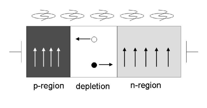
A bipolar spin-polarized solar cell Žutić et al. (2001b) is a pn junction illuminated with a circularly polarized light. See Fig. 5. The light generates both the nonequilibrium carrier density and spin. In the p region, the light generates nonequilibrium minority carriers and spin polarization by means of optical orientation. In the n region, the generated spin polarization is much lower (generally dependent on the intensity of light), a result of spin pumping. Since spin-polarized carriers are generated within the depletion layer, a spin-polarized current flows which can be used for spin injection. In addition to the density spin polarization, one is interested here in the spin current polarization , as it is this quantity that determines the spin injection efficiency. Žutić et al. (2004); Fabian et al. (2007)
The carrier and spin densities, as well as the spin polarization profiles, are shown in Fig. 6 for a generic GaAs inspired pn junction illuminated uniformly with circularly polarized light. The electron spin density follows the electron density in the p region. Here the spin orientation is rather efficient, creating about 40% spin polarization (the nominal spin polarization at electron-hole creation is 50% in zinc-blende semiconductors). In the n region, in which the density is essentially the doping density , the spin density decays from the depletion layer to the far end of the n region, where spin absorbing boundary conditions are assumed (spin Ohmic contacts). The spin is pumped into the n region by the light itself, but also by the minority channel spin pumping. The spin polarization in the n region remains small. In contrast, the spin current polarization is actually higher in the n region as compared to the p region. In the p region the polarization even changes sign, indicating a negative spin current there. All those behaviors are nicely explained by the analytical model of the generalized Shockley conditions; the model calculations are included in Fig. 6 as thin lines accompanying the numerical curves. The negative sign of , for example, is given by the positive gradient of for m. In the minority region this gradient is the only relevant contribution (that is, diffusion) to the spin current.

Since spin-polarized solar cells are envisioned for spin injection, the question arises of the I-V characteristic of the spin current. Selected characteristics are shown in Fig. 7. Let us look at the dark charge current first. The I-V curve is the typical rectification curve: there is a weak generation current at negative (reverse bias) voltages and the exponentially increasing current at positive (forward bias) voltages. In the illuminated diode this current is superimposed on the reverse current due to the photo emf.

As for the spin current, one needs to select its position in the diode. For the purposes of illustration, we choose the spin current at the far end of the diode, here at m, which would be the place of spin injection if the diode were to be used for this purpose. Another point we choose for calculating the spin current is the point at which the spin density in the n region has its maximum. From Fig. 7 we see that the magnitude of the spin current (note the sign) decreases as the voltage increases. This is due to the increased importance of spin pumping by the minority carriers at large reverse biases. The effect is more pronounced for the point of the maximum spin density, which is naturally more sensitive to the pumping.
IV Magnetic pn junction diodes and transistors
The nonmagnetic spin-polarized devices described above can be generalized to magnetic bipolar devices, most important being magnetic pn junction diodes and transistors. These employ magnetic semiconductors Dietl (2007); Jungwirth et al. (2006), which are either ferromagnetic (say, GaMnAs), or semiconductors doped with magnetic impurities, nominally paramagnetic but with giant g-factors (on the order of 100) to allow sizable spin Zeeman splitting and practical equilibrium spin polarization of the current carriers.
Magnetic pn junctions were introduced in Ref. Žutić et al., 2002, while the analytical theory of the generalized Shockley transport in such devices was laid out in Ref. Fabian et al., 2002a. The magnetic diode scheme calls naturally to be extended to a transistor (the bipolar spin transistor). Fabian et al. (2002b, 2004); Fabian and Žutić (2004, 2004, 2005); Lebedeva and Kuivalainen (2003); Flatté et al. (2003) The magnetic bipolar spintronics is in detail described in Ref. Fabian et al., 2007; we focus on the most relevant physics here, namely, the spin-charge coupling or the spin-voltaic effect. As discussed in the next section, this coupling has already been observed experimentally in magnetic pn junctions.
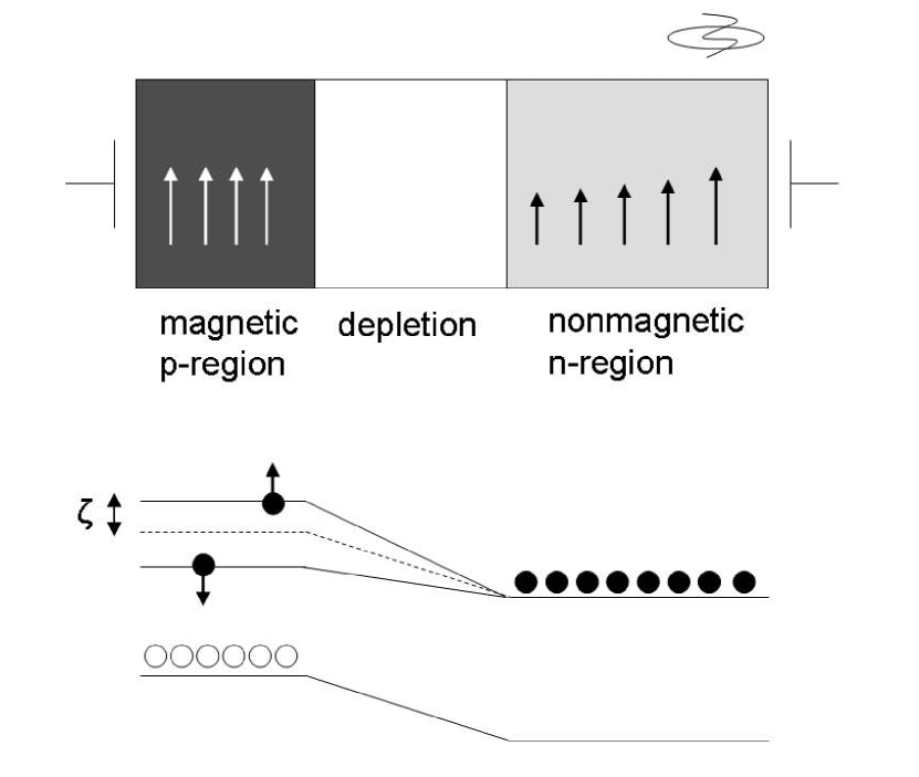
The magnetic diode depicted in Fig. 8 has a magnetic p region, seen by the spin-split conduction band, and a nonmagnetic n region. A spin source adds nonequilibrium spin in the n region. Following the spin-charge coupling idea of Silsbee and Johnson Silsbee (1980); Johnson and Silsbee (1985), we ask how is the coupling between the nonequilibrium spin and the equilibrium magnetization manifested in the I-V characteristics. While the answer is already given in Eq. 10, we reproduce a qualitative argument presented first in Ref. Fabian et al., 2002a (inspired by a similar derivation for conventional diodes in the textbook, Ref. Ashcroft and Mermin, 1976) to derive the spin-charge effect in the magnetic pn junction.
Let the electron density at the n side (here for right) of the depletion layer be and for spin up and down electrons, respectively. In terms of spin polarization , we have,
| (14) | |||||
| (15) |
The electrons in the n region need to cross a built-in electric barrier onto the p side. The effective barriers are different for spin up and down electrons,
| (16) | |||||
| (17) |
where is the intrinsic built-in barrier in the absence of the equilibrium spin splitting in the p side. In the presence of an applied bias, both barriers shift to
| (18) | |||||
| (19) |
Let us calculate the current of electrons flowing from the n to the p region. Since the electrons need to overcome the barrier, the spin up and spin down currents (so called recombination, for the label ) will be
| (20) | |||||
| (21) |
The current is simply proportional to the density of available electrons and to the Boltzmann thermionic emission factor (we are in the nondegenerate doping limit) for the probability to find the electrons of the energy needed to overcome the barrier.
Electrons also flow from the p to the n region. This flow constitutes the generation current. It is crucial to realize that this current does not depend on the applied bias . Indeed, the current is formed by the electrons created by thermal processes (excitations from a valence into the conduction band) in a proximity of the depletion layer in which they are swept into the n side. The current is not limited by the sweep, but by the generation of the carriers. For the spins in equilibrium as well as at , the individual recombination and generation currents for the given spin orientation must equal, so that no net current flows. This gives for the generation currents the following formulas:
| (22) | |||||
| (23) |
The total electron current, then is
| (24) |
where
| (25) |
is the equilibrium electron density in the p region for zero spin splitting there; nondegenerate statistics is used for expressing the equilibrium spin polarization as a function of .
While the constant is undetermined by this qualitative argument, the spin-charge coupling is manifested by the product , which is the product of the nonequilibrium and equilibrium spin. If the spins are parallel, the electron (and the total) current is enhanced; vice versa for the antiparallel spins. This gives rise to the giant magnetoresistance behavior of magnetic pn junctions. Furthermore, if the current does not vanish! The reason is that in the nonequilibrium spin converts the spin-charge coupling into current. We have termed this the spin-voltaic effect . Žutić et al. (2002); Žutić and Fabian (2003)
Magnetic pn junctions can also be used to measure all-electronically the spin relaxation time in the nonmagnetic region. The detection of would rely on the sensitivity of the residual, so called spin-voltaic current, as a function of the bias , on . The electrically injected (or optically oriented) spin source is in the nonmagnetic n region. The spin injection relies on the preservation of the nonequilibrium spin across the depletion layer. As such, the more nonequilibrium spin arrives at the depletion layer on the n side, the more it is injected into the p side. Furthermore, the zero-bias current, which is proportional to the spin-charge coupling, is proportional to the nonequilibrium spin at the depletion layer, and thus, to the spin relaxation time. The more the spin relaxes (in the nonmagnetic region) the less current there flows. The specifics are discussed in Ref. Žutić et al., 2003.
It appears that magnetic semiconductor nanostructures (say, Mn-doped quantum dots) have desirable materials properties Mackowski et al. (2004); Leger et al. (2006); Holub et al. (2004); Govorov (2005); Abolfath et al. (2007a); Savić and Vukmirović (2007); Cheng (2008) in that the strong Coulomb interactions together with the quantum confinement can increase the temperatures at which the magnetization occurs at much higher values than in the corresponding bulk Fernandez-Rossier and Brey (2004); Holub et al. (2004); Abolfath et al. (2007b) materials.
V Experimental realizations
Two experimental demonstrations of the ideas related to our proposal for the above bipolar spintronics devices have been reported: a spin-voltaic effect in a paramagnetic Kondo et al. (2006) (the employed photo diode here works as an inverse spin LED) and a ferromagnetic diode. Chen et al. (2006) In the former experiment the nonequilibrium spin is generated optically in the n region, giving rise to a spin-voltaic effect via coupling to the equilibrium paramagnetic Zeeman spin in the p region (analogous to the approach in Ref. Dery et al., 2006b). Below we describe the latter experiment Chen et al. (2006) in more detail.
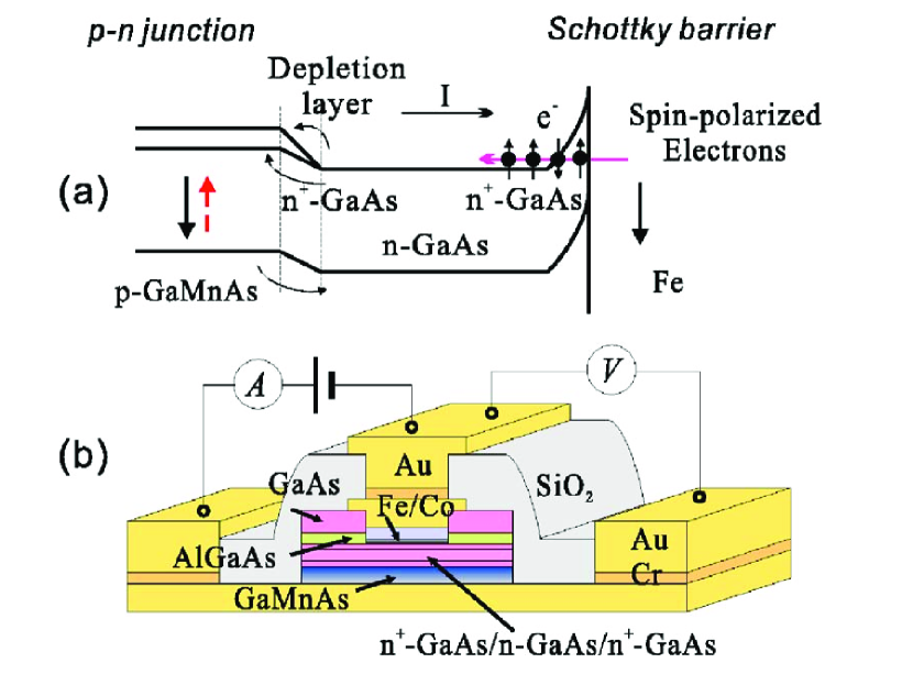
A magnetic pn junction is formed by the ferromagnetic GaMnAs, which is intrinsically p-doped (a significant portion of the 6% of Mn are acceptors) and by an n-doped GaAs, which is nominally nonmagnetic (see Fig. 9). Nonequilibrium source spin is provided by the Fe electrode, magnetically biased by Co, attached to the n-GaAs region, with the interface forming a Schottky barrier. Electrons from the Fe electrode tunnel through the barrier into the n region, bringing along spin polarization. The injected spin diffuses towards the depletion layer. There, the spin-charge coupling takes place: if the nonequilibrium spin is parallel to the equilibrium electron spin in p-GaMnAs, the current is enhanced. If the spins are antiparallel, the current is inhibited.
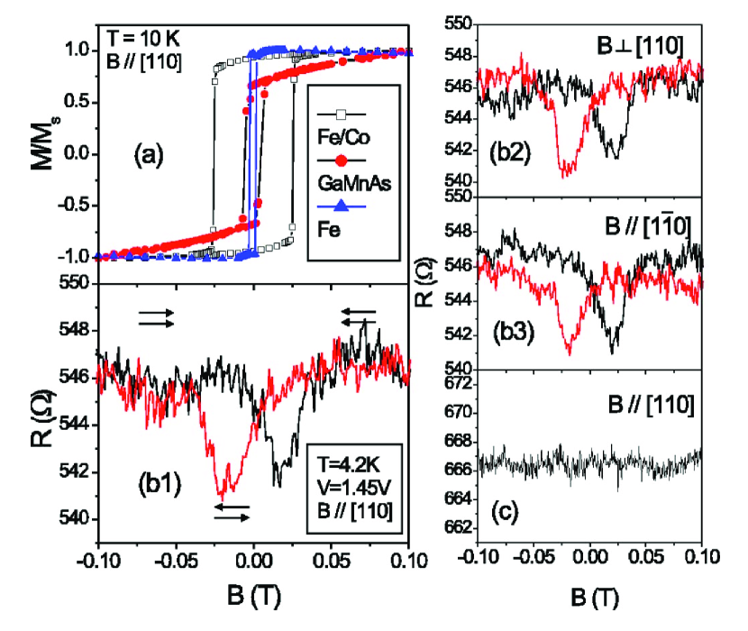
The spin-charge coupling manifests itself as a spin-voltaic effect, by producing changes in the resistance for parallel and antiparallel spin orientations of GaMnAs and the injecting Fe film. The magnetoresistance traces are plotted in Fig. 10. Since Fe and GaMnAs films used in the device have similar coercive fields, the Fe layer was biased by Co, enhancing its coercive field by an order of magnitude (to about 30 mT). This is seen in Fig. 10 a). With the biased magnetization one should see the magnetic windows with antiparallel spin orientations, in the magnetoresistance measurements. Such windows are observed in Fig. 10 b1) through b3), for different orientations of the applied magnetic field. Finally, a featureless magnetoresistance is obtained using a magnetically unbiased Fe layer, as seen in Fig. 10 c). The spin-voltaic effect has thus been demonstrated.
VI Outlook
Spin-polarized pn junctions operating under spin orientation conditions provide a particularly suitable opportunity to investigate spin transport in different regimes. In addition, the junctions present perhaps the easiest version of spintronic bipolar devices offering functionalities such as spin-polarized solar cells, for generating spin-polarized electrical currents, or spin capacitors, for control of nonequilibrium spin.
Magnetic diodes and transistors, with added source spin, offer still new functionalities based on spin-charge coupling. Indeed, magnetic pn junctions could work as giant magnetoresistive magnetic sensors, and magnetic transistors as magnetic field controlled current sources. If magnetic semiconductors are taken as desirable materials candidates for electronic applications, magnetic bipolar devices should be considered important contenders for spintronic goals of controlling electric properties by spin and vice versa.
Acknowledgements.
This work was supported by SFB 689, SPP 1285, US ONR, NSF-ECCS CAREER, CNMS at ORNL, and the CCR at SUNY Buffalo.References
- Fabian et al. (2007) J. Fabian, A. Matos-Abiague, C. Ertler, P. Stano, and I. Žutić, Acta Phys. Slov. 57, 565 (2007).
- Žutić et al. (2004) I. Žutić, J. Fabian, and S. Das Sarma, Rev. Mod. Phys. 76, 323 (2004).
- Meier and Zakharchenya (1984) (Eds.) F. Meier and B. P. Zakharchenya (Eds.), Optical Orientation (North-Holand, New York, 1984).
- Silsbee (1980) R. H. Silsbee, Bull. Magn. Reson. 2, 284 (1980).
- Johnson and Silsbee (1985) M. Johnson and R. H. Silsbee, Phys. Rev. Lett. 55, 1790 (1985).
- Tse et al. (2005) W. Tse, J. Fabian, I. Žutić, and S. Das Sarma, Phys. Rev.B 72, 241303 (2005).
- Shockley (1950) W. Shockley, Electrons and Holes in Semiconductors (D. Van Nostrand, Princeton, 1950).
- Fabian et al. (2002a) J. Fabian, I. Žutić, and S. Das Sarma, Phys. Rev. B 66, 165301 (2002a).
- Fiederling et al. (1999) R. Fiederling, M. Kleim, G. Reuscher, W. Ossau, G. Schmidt, A. Waag, and L. W. Molenkamp, Nature 402, 787 (1999).
- Fiederling et al. (2003) R. Fiederling, P. Grabs, W. Ossau, G. Schmidt, and L. W. Molenkamp, Appl. Phys. Lett. 82, 2160 (2003).
- Ohno et al. (1999) Y. Ohno, D. K. Young, B. Beschoten, F. Matsukura, H. Ohno, and D. D. Awschalom, Nature 402, 790 (1999).
- Young et al. (2002) D. K. Young, E. Johnston-Halperin, D. D. Awschalom, Y. Ohno, and H. Ohno, Appl. Phys. Lett. 80, 1598 (2002).
- Jonker et al. (2000) B. T. Jonker, Y. D. Park, B. R. Bennett, H. D. Cheong, G. Kioseoglou, and A. Petrou, Phys. Rev. B 62, 8180 (2000).
- Hanbicki et al. (2002) A. T. Hanbicki, B. T. Jonker, G. Itskos, G. Kioseoglou, and A. Petrou, Appl. Phys. Lett. 80, 1240 (2002).
- Jiang et al. (2003) X. Jiang, R. Wang, S. van Dijken, R. Shelby, R. Macfarlane, G. S. Solomon, J. Harris, and S. S. P. Parkin, Phys. Rev. Lett. 90, 256603 (2003).
- Zega et al. (2006) T. J. Zega, A. T. Hanbicki, S. C. Erwin, I. Žutić, G. Kioseoglou, C. H. Li, B. T. Jonker, and R. M. Stroud, Phys. Rev. Lett. 96, 196101 (2006).
- Kohda et al. (2001) M. Kohda, Y. Ohno, K. Takamura, F. Matsukura, and H. Ohno, Jpn. J. Appl. Phys. 40, L1274 (2001).
- Johnston-Halperin et al. (2002) Johnston-Halperin, D. Lofgreen, R. K. Kawakami, D. K. Young, L. Coldren, A. C. Gossard, and D. D. Awschalom, Phys. Rev. B 65, 41306 (2002).
- Ertler and Fabian (2006a) C. Ertler and J. Fabian, Appl. Phys. Lett. 89, 193507 (2006a).
- Ertler and Fabian (2006b) C. Ertler and J. Fabian, Appl. Phys. Lett. 89, 242101 (2006b).
- Ertler and Fabian (2007) C. Ertler and J. Fabian, Phys. Rev. B 75, 195323 (2007).
- Slobodskyy et al. (2003) A. Slobodskyy, C. Gould, T. Slobodskyy, C. R. Becker, G. Schmidt, and L. W. Molenkamp, Phys. Rev. Lett. 90, 246601 (2003).
- Petukhov et al. (2002) A. G. Petukhov, A. N. Chantis, and D. O. Demchenko, Phys. Rev. Lett. 89, 107205 (2002).
- Ertler and Fabian (2008) C. Ertler and J. Fabian, Phys. Rev. Lett. 101, 077202 (2008).
- Dery et al. (2006a) H. Dery, L. Cywinski, and L. J. Sham, Phys. Rev. B 73, 161307 (2006a).
- Dery et al. (2007) H. Dery, P. Dalal, L. Cywinski, and L. J. Sham, Nature 447, 573 (2007).
- Flatté and Vignale (2001) M. E. Flatté and G. Vignale, Appl. Phys. Lett. 78, 1273 (2001).
- Žutić et al. (2006) I. Žutić, J. Fabian, and S. C. Erwin, Phys. Rev. Lett. 97, 026602 (2006).
- Jonker et al. (2007) B. T. Jonker, G. Kioseoglou, A. T. Hanbicki, C. H. Li, and P. E. Thompson, Nature Physics 3, 542 (2007).
- van ’t Erve et al. (2007) O. M. J. van ’t Erve, A. T. Hanbicki, M. Holub, C. H. Li, C. Awo-Affouda, P. E. Thompson, and B. T. Jonker, Appl. Phys. Lett. 91, 212109 (2007).
- Appelbaum et al. (2007) I. Appelbaum, B. Huang, and J. Monsma, Nature 447, 295 (2007).
- Huang et al. (2007) B. Huang, D. J. Mosnma, and I. Appelbaum, Phys. Rev. Lett. 99, 177209 (2007).
- Žutić and Fabian (2007) I. Žutić and J. Fabian, Nature 447, 269 (2007).
- Rudolph et al. (2003) J. Rudolph, D. Hägele, H. M. Gibbs, G. Khitrova, and M. Oestreich, Appl. Phys. Lett. 82, 4516 (2003).
- Rudolph et al. (2005) J. Rudolph, S. Döhrmann, D. Hägele, and M. Oestreich, Appl. Phys. Lett. 87, 241117 (2005).
- Holub et al. (2007) M. Holub, J. Shin, D. Saha, and P. Bhattacharya, Phys. Rev. Lett. 98, 146603 (2007).
- Holub and Bhattacharya (2007) M. Holub and P. Bhattacharya, J. Phys. D 40, R179 (2007).
- Gothgen et al. (2008) C. Gothgen, R. Oszwaldowski, A. Petrou, and I. Žutić, Appl. Phys. Lett. 93, 042513 (2008).
- Žutić et al. (2001a) I. Žutić, J. Fabian, and S. Das Sarma, Phys. Rev. B 64, 121201 (2001a).
- Žutić et al. (2001b) I. Žutić, J. Fabian, and S. Das Sarma, Appl. Phys. Lett. 79, 1558 (2001b).
- Dietl (2007) T. Dietl, in Modern Aspects of Spin Physics, edited by W. Pötz, J. Fabian, and U. Hohenester (Springer, Berlin, 2007), pp. 1–46.
- Jungwirth et al. (2006) T. Jungwirth, J. Sinova, J. Mašek, J. Kučera, and A. H. MacDonald, Rev. Mod. Phys. 78, 809 (2006).
- Žutić et al. (2002) I. Žutić, J. Fabian, and S. Das Sarma, Phys. Rev. Lett. 88, 066603 (2002).
- Fabian et al. (2002b) J. Fabian, I. Žutić, and S. Das Sarma (2002b), eprint cond-mat/0211639.
- Fabian et al. (2004) J. Fabian, I. Žutić, and S. Das Sarma, Appl. Phys. Lett. 84, 85 (2004).
- Fabian and Žutić (2004) J. Fabian and I. Žutić, Phys. Rev. B 69, 115314 (2004).
- Fabian and Žutić (2004) J. Fabian and I. Žutić, Acta Phys. Polonica A 106, 109 (2004).
- Fabian and Žutić (2005) J. Fabian and I. Žutić, Appl. Phys. Lett. 86, 133506 (2005).
- Lebedeva and Kuivalainen (2003) N. Lebedeva and P. Kuivalainen, J. Appl. Phys. 93, 9845 (2003).
- Flatté et al. (2003) M. E. Flatté, Z. G. Yu, E. Johnston-Halperin, and D. D. Awschalom, Appl. Phys. Lett. 82, 4740 (2003).
- Ashcroft and Mermin (1976) N. W. Ashcroft and N. D. Mermin, Solid State Physics (Saunders, Philadelphia, 1976).
- Žutić and Fabian (2003) I. Žutić and J. Fabian, Mater. Trans., JIM 44, 2062 (2003).
- Žutić et al. (2003) I. Žutić, J. Fabian, and S. Das Sarma, Appl. Phys. Lett. 82, 221 (2003).
- Mackowski et al. (2004) S. Mackowski, T. Gurung, T. A. Nguyen, H. E. Jackson, L. M. Smith, G. Karczewski, and J. Kossut, Appl. Phys. Lett. 84, 3337 (2004).
- Leger et al. (2006) Y. Leger, L. Besombes, J. Fernandez-Rossier, L. Maingault, and H. Mariette, Phys. Rev. Lett. 97, 107401 (2006).
- Holub et al. (2004) M. Holub, S. Chakrabarti, S. Fathpour, P. Bhattacharya, Y. Lei, and S. Ghosh, Appl. Phys. Lett. 85, 973 (2004).
- Govorov (2005) A. Govorov, Phys. Rev. B 72, 075358 (2005).
- Abolfath et al. (2007a) R. M. Abolfath, P. Hawrylak, and I. Žutić, New J. Phys. 9, 353 (2007a).
- Savić and Vukmirović (2007) I. Savić and N. Vukmirović, Phys. Rev. B 76, 245307 (2007).
- Cheng (2008) S. J. Cheng, Phys. Rev. B 77, 115310 (2008).
- Fernandez-Rossier and Brey (2004) J. Fernandez-Rossier and L. Brey, Phys. Rev. Let. 93, 117201 (2004).
- Abolfath et al. (2007b) R. M. Abolfath, P. Hawrylak, and I. Žutić, Phys. Rev. Lett. 98, 207203 (2007b).
- Kondo et al. (2006) T. Kondo, J. Hayafuji, and H. Munekata, Jpn. J. Appl. Phys. 45, L663 (2006).
- Chen et al. (2006) P. Chen, J. Moser, P. Kotissek, J. Sadowski, M. Zenger, D. Weiss, and W. Wegscheider, Phys. Rev. B 74, 241302(R) (2006).
- Dery et al. (2006b) H. Dery, L. Cywinski, and L. J. Sham, J. Appl. Phys. 100, 063713 (2006b).