∎
Tel.: +358-14-260 4720
Fax: +358-14-260 4756
11email: panu.koppinen@jyu.fi
Effects of charging energy on SINIS tunnel junction thermometry
Abstract
We have investigated theoretically the effects of the charging energy to the normal metal–insulator–superconductor (NIS) tunnel junction used as a thermometer. We demonstrate by numerical calculations how the charging effects modify NIS thermometry, and how the voltage–to–temperature response and the responsivity of a current biased thermometer are affected. In addition, we show that the responsivity of the thermometer can be modulated with an additional gate electrode. The maximum responsivity is achieved when the Coulomb blockade is maximal, i.e. with a closed gate.
Keywords:
Coulomb blockade SINIS thermometry Tunnel junctionpacs:
74.78.Na 85.35.Gv 85.35.-p1 Introduction
Tunnel junction thermometry with normal metal–insulator–superconductor (NIS) junctions was discussed a while backrowellthermometry , but has only recently been widely used in low–temperature thermal transport experiments Leivomembrane ; Clelandtransport ; Photon ; karvonenPRL . Advantages of NIS thermometry are e.g. low self–heating, good responsivity, ease of integration into the system under study, small size, existing high–frequency read–out schemesRFSINIS and the fact that it can be used as local probe for temperature in nanostructures. Ideally, NIS junctions can be considered as primary thermometers, since their voltage–to–temperature (or current–to–temperature) calibration curves are determined by only two parameters: the superconducting gap and the tunneling resistance , which can be determined quite accurately from the measured current–voltage (–) characteristics of the junction. However, charging effectssinglecharge complicate this picture for small area (capacitance) tunnel junctions connected to small islands (small self–capacitance). In this case charging effects influence the voltage(or current)–to-temperature response of the thermometers, if the charging energy is of the same order of magnitude or larger than temperature, i.e. . This limit is easily obtainable in small devices, such as the recently demonstrated heat transistorheattransistor or the hybrid single electron transistorSINISSET1 ; SINISSET2 , where charging energies 1 K have been demonstrated. In this paper we investigate theoretically how affects the current biased voltage–to–temperature responsivity of the SINIS thermometer and how it can be tuned with an additional gate located in the close proximity of the junctions. For simplicity, we only concentrate on the case, where single particle tunneling is taken into account, and higher order two–particle (Andreev) processesHekking ; courtois are left out in the discussion. In addition to the charging effects, we also discuss the effect of the non–ideal single particle current caused by the broadened density of states due to the finite life–time of quasiparticles in the superconductorDynes , which causes deviations from the ideal behavior in thermometry.
2 SINIS thermometry without charging effects
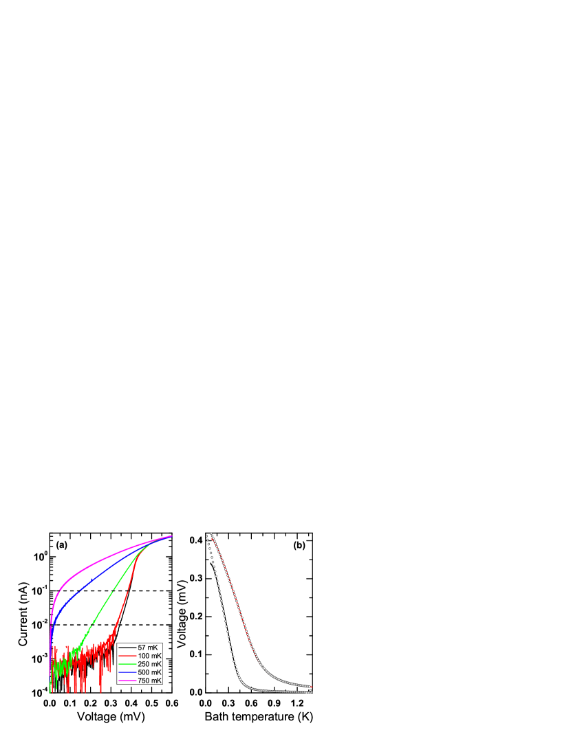
The non–linear current–voltage (-) characteristics (Fig. 1 (a)) of a NIS tunnel junction can be used for thermometry (see e.g. Jukkareview for a good review). In practice, thermometry is typically carried out by current biasing the junction at a constant current and measuring the voltage response of the thermometer, which is only a function of temperature. To obtain a larger signal, i.e. increased responsivity for thermometer, a structure containing two junctions in series (SINIS) can be used instead of a single NIS junction. Measured – curves for a typical SINIS thermometer with at different bath temperatures are shown in Fig. 1 (a). It can be seen from Figs. 1 (a) and (b) that the voltage responsivity of the thermometer can be adjusted to be optimal for a certain temperature range by adjusting the bias current: With low bias–currents ( 10 pA) there is a higher sensitivity at low–temperatures, while with higher bias–currents ( 100 pA) sensitivity is gained at high temperatures, but lost at low temperatures. The best results with thermometry are obtained by repeating experiments with a few different bias points for different temperature ranges. However, higher bias currents may cause significant heating at the lowest operating temperatures due to power dissipation to the normal metal. The practical upper limit for the bias current depends on the resistivity of the normal metal material, but is at most corresponding to voltage , after which significant heating is induced by the junction itselfJukkareview . Overheating is a critical issue at low temperatures, especially with structures containing small normal metal islands or otherwise very well thermally isolated samples, such as suspended nanowiresLT25 ; KoppinenPRL . In addition to heating, the bias current can provide self–cooling of the normal metal islandmartiniscooler ; leivocooler . Usually, SINIS junctions designed for thermometry have small junction areas and therefore small self–cooling effects, that can be neglected in the analysis (Fig. 1 (a)). However, even for larger junctions, the self–cooling can be avoided by choosing a proper bias point that never yields voltages near the optimal cooling point .
Notice also from Fig. 1 (b) that typically the measured SINIS response as a function of the refrigerator (bath) temperature deviates from the theory calculation (Eq. (2) below) at mK. This deviation is most likely due to noise heating of the electron gas, i.e. coupling of the electron gas into its electromagnetic environment causing overheating of the electrons so that . This noise heating power, typically 10 fW is dependent on the filtering of the lines in the cryostat and the electrical impedance of the junctions.
The theoretical single particle current of a NIS junction derived from the tunneling Hamiltonian is given byTinkham
| (1) |
where is the tunneling resistance of the sample, the density of states (DOS) of the superconductor and the Fermi–Dirac distributions in the normal metal and the superconductor, respectively. Interestingly, Eq. (1) can be rewritten in a symmetric form
| (2) |
where the Fermi–distribution of the superconductor is eliminated. Hence, the – is dependent only on the electron temperature of the normal metal, i.e. the NIS–junction probes directly the electron temperature of the normal metal and no additional knowledge of the temperature of the superconductor is needed. However, there is still an implicit dependence of the temperature of the superconductor, since the DOS depends on the superconducting gap, whose temperature dependence at must be taken into account. Note also that if we relax the assumption of quasiequilibrium (Fermi–function distributions) for either terminal, this simplification is not valid anymore.
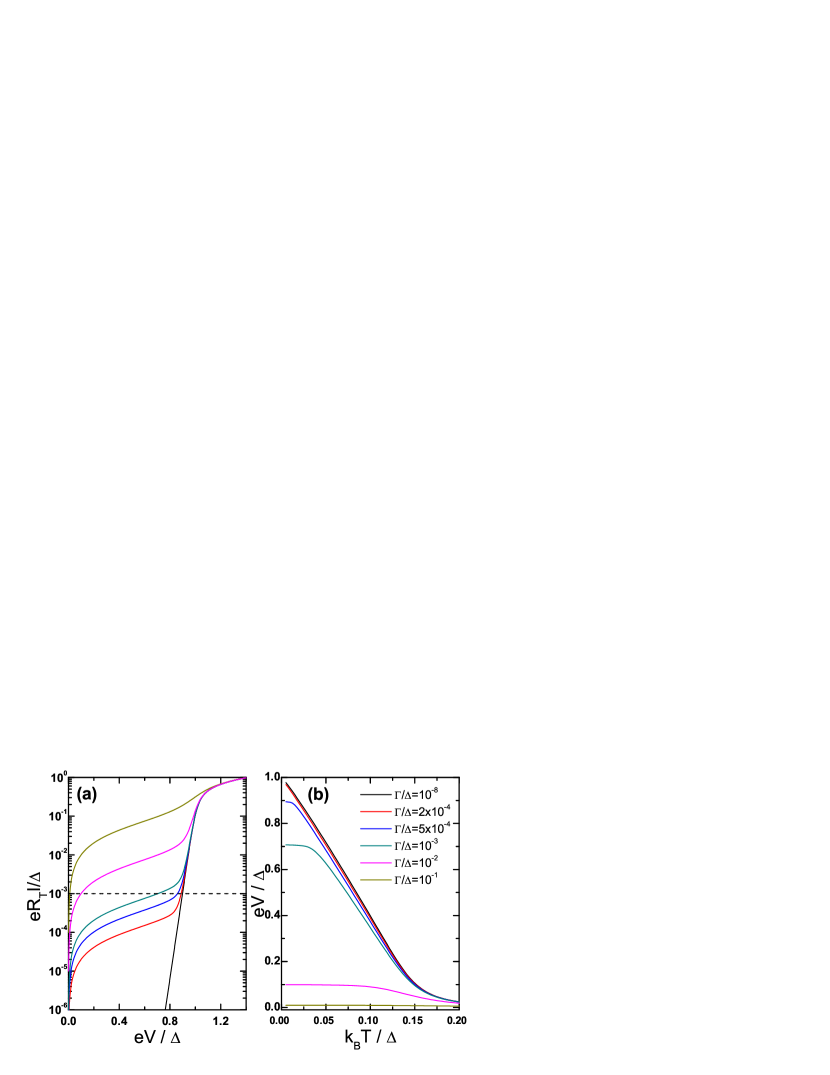
Typically, real junctions show a non–exponential finite sub–gap current (cf. Fig. 1 (a) 1 pA) at low enough temperatures and voltages. This sub–gap current can also be modelled with Eqs. (1)–(2) by incorporating a broadened DOS, i.e. by taking into account the finite life–time of quasiparticles in the superconductor Dynes . The broadened DOS is then written as
| (3) |
where describes the magnitude of broadening of the DOS. Typically for evaporated Al films we have , consistent with values reported by other groupsflyktman ; oneil . is known to depend strongly on the material quality and can be two orders of magnitude larger for evaporated Nb filmsDynesNb .
Figures 2(a) and (b) show a calculation based on Eq. (2), how the broadening of the DOS affects the – characteristics and voltage–to–temperature response of a SINIS. It is clear that the broadening of the DOS starts to influence the SINIS response mostly at low temperatures when , depending, of course, on the bias current value. At high biases, the broadening can be neglected to rather high values of but at lower biases the effect is stronger. The broadened DOS shows up in the vs. measurement qualitatively in the same way as noise heating, i.e. by leading to a saturation of the voltage at low temperatures. However, the two effects can be typically resolved in the experiment because the value for can be determined from the – characteristics, i.e. changes the current deep in the sub–gap, whereas changes the slope of the current rise at the gap edge (cf. Fig. 2(a)). Typically this broadening is not a problem for thermometry in evaporated Al films, because the bias point can be taken above the sub–gap current. However, if the SINIS thermometers are fabricated e.g. from evaporated Nb films where may be relatively high, broadening can be a real problem reducing the responsivity of the thermometers.
3 Tunneling current with charging energy
Charging effects (Coulomb blockade) due to small capacitances of the tunnel junction have an effect on thermometry, especially in the limit . We consider the case of two identical junctions in series (with the same capacitances and tunneling resistances ), i. e. a symmetric SINIS thermometer. In addition, we discuss the case where a gate electrode is in close proximity with the normal metal island, so that the geometry is basically a hybrid single electron transistor (SET) SINISSET1 . The – characteristics of SINIS structures are naturally modified when the charging effects are taken into account, and can be controlled by applying a voltage to the gatesinglecharge . The tunneling rates through a single junction with charging energy and biased with a voltage can be written asSINISSET2
| (4) | |||
| (5) |
Here the is the change in the electrostatic energy when an electron tunnels on to the island (+) and off the island (-) through junction , where stand for left and right junction, respectively. is the charging energy, where is the total capacitance of the island with the junction capacitance and the gate capacitance, is the excess quantized charge ( integer) on the island and the offset charge, which can be be varied continuously by the gate electrode voltage.
The current through the device can be calculated using these tunneling rates by solving a Master equation with the detailed balance condition
| (6) |
where and is the occupation probability of the corresponding charge state obeying the normalization condition . Once this equation is solved, the current through the island can be calculated from the expression
| (7) |
and . It can be easily shown that Eq. (7) reduces to Eq. (2) in the limit . An interesting observation about the SINIS current with a charging energy included is that it cannot be written in a form that is fully independent of the superconductor temperature , not even in the weak Coulomb blockade limit . Hence, the conclusion of Eq. (2) where a NIS junction can be used as a normal metal electron thermometer without additional knowledge of is only a special case when . This effect may be important when considering high charging energy devices used for cooling heattransistor , where temperature differences between the normal metal and the superconductor occur because of the heat flow from the island to the leads. However, for typical temperature differences mK achieved for Al based SINIS coolers, the effect on the – characteristics is only visible in the sub–gap region, and with typical bias currents it can be neglected.
4 Charging effects in thermometry
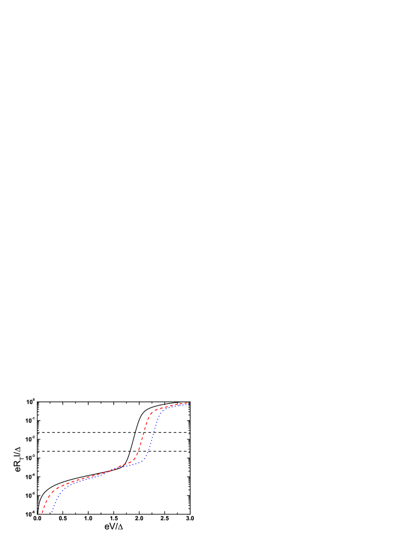
In this section we present the main theoretical results of the charging effects on thermometry and discuss how the gate can modulate the responsivity of the thermometer. All results are presented in scaled units and in all calculations the DOS broadening parameter has been used. Sub–gap – characteristics of a SINIS at temperature with three different values of charging energy 0, 0.1 and 0.2 are shown in Fig. 3. It is clear that the charging energy effectively shifts the – curves to higher voltages, leading to a behavior that resembles an effective increase of the superconducting gap from to maximally (if ). Furthermore, since the DOS is non–zero within the gap, a weak fingerprint of the Coulomb staircase can be seen in the – curves in the sub–gap region at .
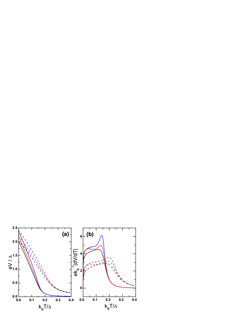
In order to study how thermometry is affected, we should investigate how the voltage-to-temperature response is modified. This is shown in figure 4(a), calculated from Eqs. (4)–(7) the same values of charging energy as used in calculating – characteristics for Fig. 3. The solid and dashed lines correspond to two different current bias values shown in Fig. 3, where the low bias , and the high bias . These scaled current values correspond to 10 pA and 100 pA currents for junctions with 50 k and = 220 µeV, typical for thin film Al. With this value of , the corresponding charging energies in Figs 3 and 4 are 0, 0.25 K and 0.5 K. The responsivities of the SINIS thermometer calculated from the voltage vs. temperature curves are presented in Fig. 4(b).
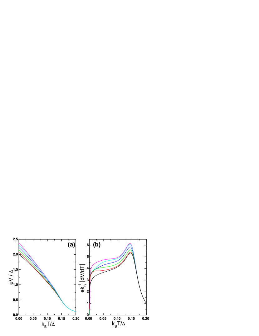
It can be seen from Fig. 4(b) that the charging energy increases the responsivity of the thermometer, but it also changes the shape of the voltage vs. temperature curve: there appears a clear bump in the responsivity curve at around for the low bias (0.2 for the high bias) when the charging energy becomes appreciable. The shift of the effective gap is also clearly seen in Fig. 4 (a) in the zero temperature limit, which moves from to . The responsivity curves also clearly show how the two different bias points have different optimal temperature ranges: at lower bias the thermometer has more responsivity for temperatures below the peak caused by charging effects (, which corresponds to mK for the values of and used above), but quickly drops to unpractically small values above that. However, at the higher bias the responsivity stays large up to much higher temperatures.
Gate modulation of the voltage response vs. temperature curves and corresponding responsivities are presented in Fig. 5(a) and (b). Here the highest value of 0.2 from the plot in Fig. 4 is used, and all curves are calculated with the low current bias value . Open and closed gate situations correspond to the top (magenta) and bottom curves (black), respectively, and gate voltages between these two extrema are plotted with an interval of . The open gate (), interestingly, has the same zero temperature limit as a thermometer with zero charging energy, however the full temperature dependent responsivity is different. This can be seen most easily from the responsivity curves in Fig. 5(b), where we see that the responsivity bump caused by still exist. Hence, the shape of the vs. curve is still different. Even more surprisingly, at low temperatures the responsivities with intermediate gate voltage values seem to merge, while the open and closed gate values are still well separated. This effect is more clearly shown in Fig.6.
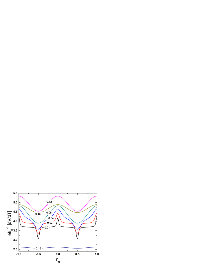
Figure 6 shows the responsivity of the thermometer as a function of the gate charge number at different temperatures from = 0.01 to 0.18. These curves were calculated with the same parameters as in Fig. 5. The low temperature results show sharply peaked values at the gate open and closed positions, while the intermediate values show flat regions, where the responsivity does not depend on the gate charge, as noted before. At higher temperatures, these sharp peaks broaden into a sinusoidal dependence whose amplitude decreases with increasing temperature. The largest change in the responsivity is obtained at the lowest temperatures, where responsivity can be enchanced by 30 by closing the gate at , for example.
5 Relevance to experiments
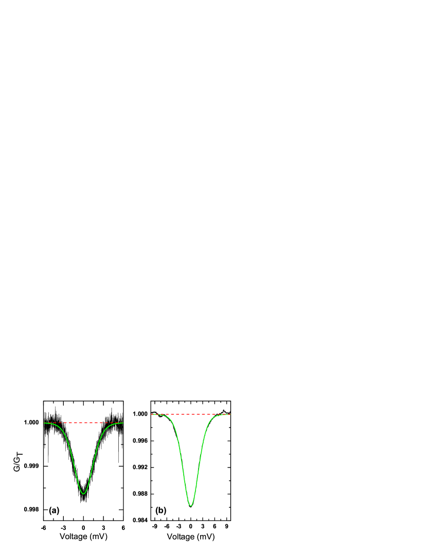
To decide in practice when one should consider Coulomb charging in SINIS thermometry, one needs to measure the value of the charging energy and compare it with the temperature range of interest. The measurement can easily be performed at 4.2 K in the weak Coulomb blockade () limit, where the size of the zero bias Coulomb blockade dip in the tunneling conductance spectrum depends on the charging energy by the relation Jukkareview
| (8) |
where is the tunneling conductance around without the dip. As an example, figure 7 shows two measured Coulomb blockade dips at 4.2 K with (a) a typical larger junction area (0.35 µm2) Al/Cu/Al SINIS device designed to act as a cooler LT25 ; KoppinenPRL , and (b) a smaller typical solitary Al/Cu/Al SINIS thermometer with a junction area µm2. From the measurements we obtain 20 mK for the cooler sample, showing that it is in the limit of weak Coulomb blockade for our experimentally achievable (dilution refrigerator) temperature range. The changes to the voltage-to-temperature response are within the experimental error in that case, and analysis can be carried out with the simpler theory of Eq. (2), without charging effects.
However, the effects of charging energy are more observable in the second, smaller SINIS thermometer (5 µm x 300 nm x 30 nm normal metal island), with a measured charging energy 200 mK (Fig. 7 (b)). This type of thermometer is typically used e.g. for probing the bath or (local)phonon temperature during an experiment. The measured corresponds to a value for Al, which leads to observable changes in the temperature response based on the calculations in the previous section.
6 Conclusions
We have studied the charging effects on SINIS tunnel junction thermometry and shown that for small enough junctions, the responsivity of the thermometer can be modulated with an additional gate electrode in close proximity to the junctions, with maximum responsivity achieved with the closed gate situation. In addition, the shape of the voltage response vs. temperature curve changes when the charging energy is taken into account, leading to the conclusion that in typical solitary SINIS thermometers charging effects must be taken into account in the conversion from measured voltage to temperature (calibration), and have to be computed numerically. The effect of an unknown offset charge will not lead to ambiguities in the analysis, as the shape of the voltage vs. temperature curve changes as a function of the offset charge, so that the value of the offset charge can be determined self-consistently.
Acknowledgements.
P.J.K. acknowledges Magnus Ehrnrooth foundation and T.K. acknowledges Emil Aaltonen foundation for financial support. We thank J. Pekola for discussions. This work has been supported by the Academy of Finland projects No. 118665 and 118231.References
- (1) J.M. Rowell, D.C. Tsui, Phys. Rev. B 14, 2456 (1976)
- (2) M.M. Leivo, J.P. Pekola, Appl. Phys. Lett. 72, 1305 (1998)
- (3) C.S. Yung, D.R. Schmidt, A.N. Cleland, Appl. Phys. Lett. 81, 31 (2002)
- (4) M. Meschke, W. Guichard, J.P. Pekola, Nature 444, 187 (2006)
- (5) J.T. Karvonen, I.J. Maasilta, Phys. Rev. Lett. 99, 145503 (2007)
- (6) D.R. Schmidt, C.S. Yung, A.N. Cleland, Appl. Phys. Lett. 83, 1002 (2003)
- (7) H. Grabert, M.H. Devoret, Single Charge Tunneling: Coulomb Blockade Phenomena In Nanostructures (Plenum Press, New York, 1992)
- (8) O.P. Saira, M. Meschke, F. Giazotto, A.M. Savin, M. Möttönen, J.P. Pekola, Phys. Rev. Lett. 99, 027203 (2007)
- (9) J.P. Pekola, J.J. Vartiainen, M. Möttönen, O.P. Saira, M. Meschke, D.V. Averin, Nature Phys. 4, 120 (2008)
- (10) A. Kemppinen, M. Meschke, M. Möttönen, D.V. Averin, J.P. Pekola, arXiv:0803.1563 (2008)
- (11) F.W.J. Hekking, Y.V. Nazarov, Phys. Rev. B 49, 6847 (1994)
- (12) S. Rajauria, P. Gandit, T. Fournier, F.W.J. Hekking, B. Pannetier, H. Courtois, Phys. Rev. Lett. 100, 207002 (2008)
- (13) R.C. Dynes, J.P. Garno, G.B. Hertel, T.P. Orlando, Phys. Rev. Lett. 53, 2437 (1984)
- (14) F. Giazotto, T.T. Heikkilä, A. Luukanen, A.M. Savin, J.P. Pekola, Rev. Mod. Phys. 78, 217 (2006)
- (15) P.J. Koppinen, I.J. Maasilta, J. Phys.: Conf. Ser. 150, 012025 (2009)
- (16) P.J. Koppinen, I. J. Maasilta, Phys. Rev. Lett. in press (2009), arXiv: 0901.2895
- (17) M. Nahum, T.M. Elles, J.M. Martinis, Appl. Phys. Lett. 65, 3123 (1994)
- (18) M.M. Leivo, J.P. Pekola, D. Averin, Appl. Phys. Lett. 68, 1996 (1996)
- (19) M. Tinkham, Introduction to superconductivity, 2nd Ed. (McGraw–Hill, New York, 1996)
- (20) J.P. Pekola, T.T. Heikkilä, A.M. Savin, J.T. Flyktman, F. Giazotto, F.W.J. Hekking, Phys. Rev. Lett. 92, 056804 (2004)
- (21) G.C. O’Neil, D.R. Schmidt, N.A. Miller, J.N. Ullom, K.D. Irwin, A. Williams, G.B. Arnold, S.T. Ruggiero, J. Low. Temp. Phys. 151, 70 (2008)
- (22) J.J. Toppari, T. Kühn, A.P. Halvari, G.S. Paraoanu, J. Phys.: Conf. Ser. 150, 022088 (2009)