Deposition of Diamond-like Carbon films using Dense Plasma Focus
Abstract
Diamond Like Carbon (DLC) films were deposited on quartz substrates using Dense Plasma Focus (DPF) method. The formation of bonds as is it’s content in the film strongly depends on the substrate and it seems quartz is not a suitable substrate. However, we report here the formation of DLC films on quartz substrates that were maintained at elevated temperatures and show the content of carbon atoms with bonds in the film is directly proportional to the substrate’s temperature. Not only does this give good control of film fabrication, but also shows how to take advantage of DLC film’s anti-wear, scratch resistant properties on material surfaces that require protection.
PACs No: 81.05.Uw, 78.55.Qr, 78.20.-e
Introduction
Carbon exists in various allotropic forms in nature of which the two most popular states are the trigonally bonded () graphite form and the tetragonal bonded () diamond form. Since the last decade, the amorphous mixture containing significant fraction of diamond like bonded carbon intimately mixed with graphite has been studied. Due to the unique features exhibited by this mixture, this form is now catagorized as Diamond like Carbon (DLC). The term DLC was first used by Aisenberg and Chabot [1]. In contrast to amorphous carbons, this new form of carbon is hard, electrically insulating and wear resistant. That is, though DLC exhibits Diamond like properties it lacks the crystallinity of diamond.
Due to its unique structural, mechanical, optical and electronic properties, DLC films have wide range of potential applications [2]. They are used for anti-reflection and protective coatings in IR and UV optics and tribological applications such as a mechanically hard, scratch resistant layer to coat cutting tools so as to protect them against corrosion and wear. DLC films also have potential application for electronic packaging, passivation and thermal heat sinks for high power devices because of their high thermal conductivity and electrical resistivity. Being biocompatible, wear resistant, and chemically inert, DLC films are also used to coat heart valves, rods inserted inside human limbs and contact lenses. Interestingly, the properties of this form of carbon is strongly dependent on the ratio in the mixed structure.
The potential applications of DLC films have stimulated a great deal of interest in present decade. Various methods have been developed to deposit DLC films, like DC sputtering [3], RF sputtering [4], magnetron sputtering [5, 6], ion beam sputtering [7, 8], plasma assisted physical vapour deposition [9], plasma assisted chemical vapour deposition [10], ion beam deposition [1],[11]-[13], fast atomic beam bombardment (FAB) technique [14], carbon arc evaporation [15, 16], laser evaporation [17, 18], (VHF PECVD) technique [19] and more recently by Dense Plasma Focussing (DPF) [20, 21].
A common feature of all the methods mentioned above is that the DLC film is condensed from a beam containing medium energy 100eV carbon or hydrocarbon ions. In this paper we discuss the deposition of DLC films by a Dense Plasma Focus (DPF) device where the beam energy is considerably higher. In the following passages we report the results of various characterisation done on the DLC films deposited by DPF. Also, it is worth mentioning here that in the present study we have used quartz substrates unlike the earlier reports on DLC film fabrication using DPF [20, 21] where silicon wafers were used as substrates.
1 Experimental Details
We have used a Mather type DPF device of available in the Plasma research laboratory of Delhi University. The geometry of the DPF Device and its working is detailed elsewhere [22]-[28]. The Dense Plasma Focus Device (DPF) produces energetic (1-2 keV) high-density plasma for duration of about hundred nanoseconds [17, 18, 22]. The chamber was evacuated and filled with Argon gas with the pressure inside the chamber maintained in the range of 80-120 Pa. Energetic ions move from source to substrate in a cylindrical geometry along the axial direction of central electrode. These highly energetic carbon ions were deposited on quartz substrates placed at the top of the chamber. DLC films were thus obtained on quartz substrates maintained at different temperatures.
The deposition rate of our apparatus in the present study (arrangement) was found to be 450Å per shot. All our samples were grown with four focused shots of carbon ions from Dense Plasma Focus device. Each DPF shot was of 100ns duration. Thus, the average thickness of the our films were 1800Å. The thickness of the films were measured and confirmed using a Dektak profilometer. The profilometer also showed the films to have a smooth topography with low surface roughness.
The structural and morphological analyses of our films were carried out. X-Ray diffraction studies of the films were carried out using Phillips PW-1840 X-ray diffractometer. The SEM micrographs of our films, taken using JEOL JSM-1840 Scanning Electron Microscope.
2 Results and Discussions
Visual examination showed the film grown at room temperature to be blackish in color. This is characteristic of graphite films. However, films grown on substrates maintained between temperatures and were found to be transparent. The transparent films were found to be scratch resistant and chemically inert. Chemical inertance is based on our test of applying drops of concentrated hydro-chlorine acid (HCl) and nitric acid () on the film’s surface. The films showed remarkable stability. Also, the films showed no sign of disintegration or peeling even after months of deposition. This stability and the transparent nature of the films grown on quartz substrates kept at elevated temperatures indicate the formation of DLC films. In the following sections we report the structural and optical characterisation of these samples which would prove the formation of DLC films.
2.1 Structural and Morphological Studies
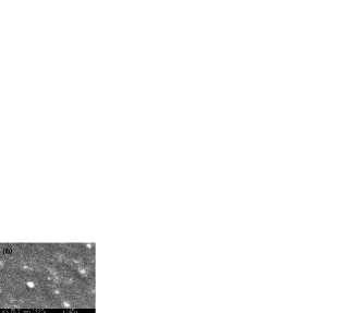
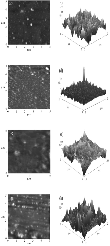
As expected the diffractograms of the films grown at room temperature and at higher temperature showed them to be amorphous in nature without exception (fig 1). The hump seen in the X-ray diffractogram however is indicative of some short range ordering among the atoms of the films. The morphological study is indicative of this with no features evident on the films surface when examined under scanning electron microscope (fig 2a). The blackish asgrown films showed granularity with grain sizes of the order of 100nm. The Atomic force microscope (AFM) image of the samples surface confirms the surfaces granularity (fig 3a). One would expect X-Ray diffraction peaks if ordering of atoms takes place over larger distances accompaning increase in grain size. However, the surface of the transparent films obtained by growing them on heated substrates did not exhibit features similar to that obtained in asgrown films (fig 2b). The grains are small, sparse and scattered as can also be seen from the AFM images of the films grown on heated substrates (fig 3). Also, notice the surface roughness is minimum for the film grown on substrates maintained at . We believe the surface roughness may be an important contributing factor in the optical properties of the films that we investigate in the following section.
3 Optical Properties
3.1 Raman Studies
The Raman spectra have been recorded at room temperature with 514.5nm line of a spectra Physics 2030 laser in the backscattering geometry. A laser beam of 5mW power was used. The spectra were recorded with a Spex Triplemate recorder. Fig 4 shows the Raman spectra of the DLC films deposited by DPF device on quartz substrates kept at , and respectively. The broad peak and corresponding to the G band and D band overlap and have been deconvoluted. Deconvolution enables us to estimate the Peak Position, Area, Maximum Intensity and the Full Width at Half Maxima (FWHM) of each band. The results are listed in Table 1. The G peak’s FWHM is a measure of disorder of bond angles in graphites. This is a measure of the stress in the samples. Robertson [29] states that the Raman peak’s position decreases linearly with increasing stress. In other words,
| D line | G line | |||||||
|---|---|---|---|---|---|---|---|---|
| Temp. | Center | Int. | Area | FWHM | Center | Int. | Area | FWHM |
| 1340 | 1509 | 256.6 | 1600 | 1912 | 68.7 | |||
| 1339.6 | 3063 | 221 | 1594.6 | 3925 | 73.6 | |||
| 1357.7 | 8567 | 251.06 | 1584.2 | 9837 | 100.94 | |||
This is true in our samples, where there is an increase in the G peak’s FWHM accompanied with a decrease in the peak position as the substrate’s temperature is raised. This implies that with increased substrate temperature, the stress in the film (in terms of disorder in graphite bond angles) increased. Beeman modelled [30] DLC films and predicted that the increasing diamond like structure generates stress within the film. That is, the shifting of the ‘G’ peak is also an indication of the formation of bonds.
The content have also be estimated from the ratio of areas enclosed by the two peaks. The ratio is also said to be inversely proportional to the fractional ratio of bonded material present to that of bonded carbon [29]. However, in our case decreased from to 0.78 for increase in substrate temperature from to and subsequently increased to 0.87 for films grown on substrates maintained at . This suggests an increase in content followed by a decrease with substrate heating. Singha [31] et al however consider the ratio to be a poor measure of the content.
Ferrari and Robertson [32] have characterised the formation of DLC in three stages (a) stage 1 that of NC carbon, (b) stage 2 that of a-carbon and (c) stage 3 of ta-carbon. Each stage is well identifiable using their Raman spectras. As per this model our DLC samples are of stage 2, having their G peak position between 1600 to 1510 and the ratio of peak intensities, between 0.25 to 2. Stage 2 films are also marked by ‘G’ peaks with FWHM greater than indicative of grain size of the order of 1nm. AFM images (fig 3) also substantiate that our samples can be classified in stage 2. Using data from Ferrari and Robertson [32] and that of Tamor et al [33], Singha et al [31] gives the content of in DLC samples of stage 2 as
| (1) |
where is the position of the Raman ‘G’ peak. Calculating the percentage of in our samples using eqn(1) and data listed in Table I, we find that content of increased from 14.22% to 22% as the substrate temperature was increased. A plot of content with respect to substrate temperature (fig 5) shows perfect linearity. Thus, good control over the quality of DLC films can be obtained by controlling the substrate temperature.
To compare contribution of substrate on DLC formation, we placed a silicon substrate along with the quartz substrate and maintained both at . Deposition of films were done simultaneously and yet the film grown on silicon (fig 6) had 30.36% of carbon atoms with bondings as compared to just 22% obtained on the quartz substrates (fig 4c). This maybe a result of dangling bonds of silicon on the wafer surface acting as center of seeding, encouraging formation of bondings.
3.2 UV Spectroscopy
The transmission spectra of the DLC films were obtained using Shamadzu UV-260 spectrophotometer. Fig 7 shows the variation of transmittance (percentage) of the films deposited at various substrate temperatures. As expected the graphite films grown at room temperature with it’s opaqacity has the lowest transmittance. The nature of the curves in fig 7 suggests that the band gaps of the flms lie in the UV region. Hence, we have not attempted to calculate Tauc’s bandgap from this data.
The films grown at and have very similar amount of atoms in bondings and yet their transmittance is sharply different. We believe the surface smoothness of samples grown at show better transmission due to lower surface scattering. As the surface roughness increases (for sample ‘d’, grown on substrate kept at ), the transmittance decreases.
4 Conclusion
To conclude, we have deposited Diamond like Carbon films using Dense Plasma Focus Device on quartz substrate at moderate temperatures. Till now DLC films have been fabricated by various methods on Silicon substrates by varying the beam energy. This technique shows that good quality films can be grown on different substrates and simple method of varying substrate temperature not only gives DLC films but also gives a control over the optical properties of the resulting film. This gives true meaning to the tribological applications of DLC films where it can be grown on any surface that requires mechanical/ scratch resistant properties.
5 Acknowledgment
We are thankful to Mr. N.C. Mehra and Raman Malhotra University Science and Instrumentation Center (USIC), Delhi University, for carrying out the analysis of our samples.
References
- [1] S.Aisenberg and R.Chabot, J.Appl.Phys., 42, 2953 (1971).
- [2] H.Dimigen, H.Hubsch and R.Memming, Appl. Phys. Lett., 50, 1056 (1987).
- [3] A.G.Fitzgerald, M.Simpson, G.A.Dederski, P.A.Moir, A.Matthews and D.Tither, Carbon, 26, 229 (1988).
- [4] J.Ullman, G.Schmidt and W.Schraff, Thin Solid Films 214, 35 (1992).
- [5] E.Eldrige, G.A.Clarke, Y.Xie and R.R.Parsons, Thin Solid Films 280, 130 (1996).
- [6] N.H.Cho, K.M.Krishnan, D.K.Veirs, M.D.Rubin, C.B.Hooper, B.Bunshah and D.B.Bogy, J.Mater.Res. 5, 2543(1990).
- [7] C.Weissmantel, C.Schurer, F.Frolich, P.Grau and H.Lehman, Thin Solid Films 61, L5 (1979).
- [8] J.J.Cuomo, J.P.Doyle, J.Bruley and J.C.Liu, J.Vac.Sci.Technol. A9, 2210 (1991).
- [9] J.Smith, A. Dehbi and A.Matthews, Relat. Mater. 1,355 (1992).
- [10] F.Akatsuka, Y.Hirose and K.Komaki, Jpn. J. Appl. Phys., 27, L1(1988).
- [11] J.Koskinen, J.Appl.Phys. 63, 2094 (1988).
- [12] F.Rossi, B.Andre, A. Van Even et.al. Appl. Phys.75, 3121 (1994).
- [13] D.Tither, A. Matthews, A.G.Fitzgerald, B.E.Storey, A.E.Henderson, P.A.Moir et.al. Carbon 27, 899(1990).
- [14] A.S.A.Voevodin, J.M.Schneider, C.Capera, P.Stevenson and A. Matthews, Vacuum 46, 299 (1995).
- [15] I.Aksenov, V.A.Padalka and V.M.Khoroshikh, Sov. Plasma Phys. 4, 425 (1978).
- [16] P.J.Martin, S.W.Fillipezuk, R.P.Netterfield, J.S.Field, D.S.Whitmell and D.R.McKenzie, J.Mater. Sci.Lett. 7, 410(1998).
- [17] C.B.Collins, F.Davantoo, D.R.Jander, T.J.Lee, H.Park and J.H.You, J.Appl.Phys. 69, 7862 (1991).
- [18] F.Davanloo, E.M.Juengerman, D.R.Jander, T.J.Lee and C.B.Collins, J.Mater.Res. 5, 2398 (1990).
- [19] Sushil Kumar, P.N.Dixit, D.Sarangi and R. Bhattacharyya, J.Appl.Phys. 93, 6361(2003).
- [20] Shaista Zeb, Mehboob Sadiq, A. Qayyum, Ghulam Murtaza, M. Zukaullah, Materials Chemistry and Physics 103, 235-240 (2007).
- [21] L.Y.Soh, P.Lee, X.Shuyan, S.Lee and R.S.Rawat, IEEE Trans. Plasma Sci. 32, 448-453 (2004).
- [22] J.W.Mather, Phys. Fluids 7, 5 (1964).
- [23] Chayya R.Kant, M.P.Srivastava and R.S.Rawat, Phys. Lett.A226, 212(1997).
- [24] Chayya R.Kant, M.P.Srivastava and R.S.Rawat, Phys. Lett A239, 109 (1998).
- [25] R.S.Rawat, M.P.Srivastava, S.Tandon and A.Mansingh, Phys.Rev.
- [26] M.P.Srivastava, S.R.Mohanty, S.Annapoorni and R.S.Rawat, Phys. Lett. A215, 63 (1996).
- [27] P.Agarwala, S.Annapoorni, M.P.Srivastava, R.S.Rawat and Pratima Chauhan, Phys. Lett. A231, 434(1997).
- [28] R.Sagar and M.P.Srivastava, Phys. Lett.A183, 209 (1993).
- [29] J. Robertson, Mat. Sci. Eng. R, 37, 129 (2002).
- [30] D.Beeman, R.Lynds, M.R.Anderson, Phys. Rev. B. 30 870 (1988).
- [31] Achintya Singha, Adidti Ghosh, Nihar Ranjan Ray and Anushree Roy, arXiv:cond-mat/0601030v1.
- [32] A.C.Ferrari and J.Robertson, Phys. Rev. B 61, 14095 (2000).
- [33] M.A.Tamor and W.C.Vassell, J. Appl. Phys. 76, 3823 (1994).
Figure Captions
-
1
X-ray diffractogram of DLC film prepared on substrates maintained at .
-
2
Scanning Electron Micrograph of DLC film prepared at (a) room temperature and (b) on substrates maintained at .
-
3
Atomic Force Microscope images of DLC film prepared at (a) room temperature, (c) on substrates maintained at , (e) on substrates maintained at and (g) on substrates maintained at . Images (b), (d), (f) and (h) are the 3-D view giving an idea of the film surface’s roughness shown in (a), (c), (e) and (g) respectively.
-
4
Raman Spectra of DLC films deposited on quartz substrates maintained at temperature (a) , (b) and (c) . The deconvulated curves represents the D and G peaks.
-
5
The content of carbon atoms with bondings increases linearly with temperature at which the quartz substrates were maintained.
-
6
Raman Spectra of DLC films deposited on Silicon substrates maintained at . The deconvulated curves represents the D and G peaks. The peak between 900-1000 is of silicon from the substrate.
-
7
The UV-visisble transmission spectra of DLC films deposited on quartz substrates maintained at temperature (a) room temperature, (b) , (c) and (d) .
Figures


