Nanoparticle networks as chemoselective sensing devices
Abstract
We theoretically analyzed transport properties of a molecular network constructed of gold nanoparticles linked with oligophenylenevinulene (OPV) molecules. We showed that the conductance of such system was strongly reduced when trinitrotoluene (TNT) became attached to the OPV linkers in the network. The reported results are based on the ab initio electronic structure calculations. These results corroborate and elucidate experiments which revealed significant drops in the conductance the network while the latter was exposed to TNT vapors. The results suggest that the detected sensitivity of transport characteristics of the considered nanoparticle network to TNT may be used to design a sensing nanodevice.
pacs:
73.63.Rt, 73.23.Ad, 31.15.A-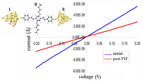
Molecular-scale conductors attract significant interest and attention in both fundamental and application research during the last two decades 1 ; 2 ; 3 ; 4 . The unceasing interest of the research community to these conductors originates from their actual and potential usefulness in inventing and designing various nanodevices. In particular, the integration of nanotechnology with molecular recognition poses numerous possibilities for creation of novel sensing devices 5 ; 6 ; 7 ; 8 ; 9 ; 10 . Significant efforts are being applied to study electron transport in networks made out of nanoparticles connected by linker molecules 11 ; 12 ; 13 ; 14 ; 15 ; 16 . It is both interesting and important to investigate their potential in designing molecule recognizing sensors.
The present work is motivated by recent experiments carried out to explore transport properties of a three-dimensional molecular network consisting of gold nanoparticles linked by oligophenylenevinulene (OPV) molecules. The molecular network was built using a cowpea mosaic virus (CPMV) as a scaffold. The CPMV is a particle of an icosahedral geometry made out of sixty copies of a protein subunit whose average diameter is about as was determined by -ray crystallographical analysis 17 . To use the CPMV as a scaffold for the molecular network it was genetically engineered in order to provide cystein residues at selected positions. Gold nanoparticles with diameters were bound to these residues. Due to the icosahedral symmetry of the virus the residues and attached gold particles are arranged into complex three dimensional structure of the same symmetry. The latter determines interparticle distances. The CPMVs decorated with gold nanoparticles were exposed to OPV molecules which linked the gold particles producing conductive network on the viruses.
To measure the conductance of a network built on a single virus the latter was assembled between proximal probe electrodes. The electrodes were made out of pair of wide gold leads patterned on a silicon wafer. After measuring the baseline conduction, the entire chip was exposed to the target, and the transport measurements were repeated after binding the target. Actually the test chip included several pairs of electrodes which allowed statistical analysis of the results. Strong changes in the network conduction were observed when the latter was exposed to trinitrotoluene (TNT) vapors. The exposure resulted in a significant decrease in the conduction (Fig. 1). This conduction decrease occurred at rather small values of the bias voltage applied across the network The experimentally disclosed sensitivity of the above described molecular network to TNT makes it potentially useful to design a TNT sensing nanodevice.
To theoretically analyze and explain these experimental results we computed eigenenergies and corresponding wave functions for the molecular network element including two gold nanoparticles connected by the OPV molecule both with and without attached TNT. We did perform full self-consistent computations using the NRLMOL software package 18 . In addition to self-consistently solving the Kohn-Sham equations we have optimized the geometries of the examined molecules. Once we arrived at the resulting Hamiltonian matrices we proceeded using Lowden’s method 19 of symmetrical orthogonormalization to build up atom centered Wannier-like wave functions 20 starting from the nonorthogonal gaussian orbitals. Using these as a new basis functions we reconstructed the Hamiltonian matrices. Now, the matrices became nearly diagonal enabling us to separate out three diagonalized blocks corresponding to the left and right gold nanoparticles and the molecule in between. Small off-diagonal elements in the resulting Hamiltonian matrices between the and blocks describe the coupling of the molecular linker to the gold nanoclusters in the considered network.
The final matrices used in the following transport calculations are obtained separating out those parts of the Hamiltonian matrices which could be placed in the window around the equilibrium Fermi energies The window width is determined by the value of the bias voltage. So, the full Hamiltonian matrices are replaced by these reduced matrices of relatively small dimensionalities. This procedure is justified for only those states whose eigenenergies are rather close to the Fermi energy could actually contribute to the electron transport.
In our transport calculations we employ the effective Hamiltonian for the molecule linking two adjacent metal nanoparticles. The latter is written in the usual form (see e.g. Refs. 21 ; 22 ):
| (1) |
Here, the term corresponds to the molecule, and describe the coupling of the molecule to the gold nanoclusters. Omitting for a while the last two terms and keeping in mind that the orbitals included into the basis set are orthogonormalized, we may introduce the retarded Green’s function for the single molecule 2 . The latter is defined by the matrix equation:
| (2) |
where is the identity matrix. The parameter describes the broadening of the molecule energy levels due to random motions of the surroundings at finite temperature and takes on values of the order of thermal energy
To proceed we employ the Dyson equation relating the retarded Green’s function of the molecule coupled to the metal nanoclusters to the Green’s function of a single molecule. The equation reads 23 :
| (3) |
Within the chosen basis set of the wavefunctions the matrix is a diagonal matrix
| (4) |
where are the eigenenergies of the molecule.
In the Eq. (3), the self-energy term characterizes the coupling of the molecule to the left and right nanoclusters:
| (5) |
The matrix elements of self-energy corrections have the form 1 :
| (6) |
Here, are, respectively, the coupling strengths between -th molecule state and -th state on the left/right metallic cluster, are energy levels of the corresponding nanoclusters, and the parameters describe the thermal broadening of the electron levels at the clusters. The summation over in the Eq. (6) is carried out over the states of the left/right cluster.
When the bias voltage is applied across the system shown in the Fig. 1, this causes charge redistribution, and subsequent changes in the energies and In consequence, the matrix elements and values vary as changes. This affects the electron transmission function given by the expression:
| (7) |
where and is the advanced Green’s function of the molecule . Nevertheless, our computations showed that at low bias voltage values its effect on the electron transmission is weak and may be neglected. Therefore, in further analysis we use the expression for the electron transmission function computed at We remark, that the self-energy parts given by Eq. (6) depend on the values of representing electron structures of the gold nanoclusters, and on temperature inserted in the terms . So, the changes in the electron structure of the clusters may affect the transmission as well as the changes in the electron structure of the linking molecule. The latter is included in the expressions for the Green’s functions
Now, we employ the standard expression for the electron tunneling current flowing through the molecule 2 :
| (8) |
Here, is the electron charge, is the Planck’s constant, is the electron transmission given by Eq. (7), is the Fermi distribution function for the energy Chemical potentials are attributed to the left/right nanoparticles, and they are shifted from the equilibrium Fermi energy due to the bias voltage applied across the system:
| (9) |
where is the division parameter which shows how the voltage is distributed between the nanoclusters.
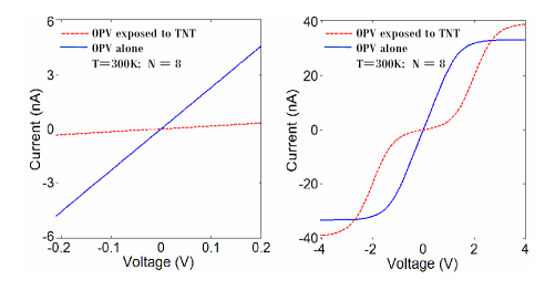
We applied Eqs. (7)-(9) compute to the tunneling electron current through a part of the experimentally studied network. The chosen part included eight pieces connected in series, each piece consisting of two gold nanoparticles linked by a molecule. The number of pieces roughly corresponds to the number of gold nanoparticles set along the half of the CPMV circumference. We assumed the bias voltage to be applied across the whole chain, so the voltage across two adjacent gold clusters appeared to be smaller than the net voltage Supposing that all molecular links in the chain are the OPV molecules and none of these are loaded with TNT, we did obtain the current-voltage characteristics shown as solid lines in the Fig. 2. At low bias voltage the characteristic is an ohmic curve which strongly resembles the experimental curve (see Fig. 1). Both experimental and calculated curves are symmetrical, and the computed current takes on values close to those observed at the same bias voltage, as follows from comparison of the figures and (left panel). When TNT molecules are attached to all OPVs included in the chain, our calculations result in the critical reduction of the conductance at low bias voltage as presented in the Fig. 2. This agrees with the experimental results.
We remark, that computed drop in conductance significantly exceeds that observed in the experiments. The mismatch could be reduced if we assume that TNT molecules are attached to some OPV linkers in the network not to everyone. Within the chosen model we can show that the decrease in the number of TNTs attached to the OPV linkers brings enhancement in the conductance of the chain which manifests itself as the increase in the slope of the relevant characteristics at low bias. The corresponding lines would be positioned between the dashed and the solid lines in the left panel of the figure and the smaller is the number of TNT-OPV complexes the closer is the characteristics to the solid line. The latter corresponds to the chain of gold nanoparticles linked by OPVs alone.
At higher voltage the conductance of the OPV-TNT molecular complexes enhances and becomes greater than the conductance of single OPV molecules. As follows from our calculations, at the energies close to self-energy terms accept smaller values for joint molecular linkers than for single OPVs connecting gold nanoparticles in the network. The current between the nanoparticlies is defined by Eq. (8), and at low values of the applied voltage energies close to give the predominating contribution to the relevant integral. So, the reduction in results in the reduction of the conductance at low bias voltage.
Finally, in the present work we studied transport properties of the network consisting of gold nanoparticles linked by OPV molecules. These studies were motivated by the experimental results which revealed strong sensitivity of this system to TNT vapors. We carried out ab initio electronic structure calculations for the network element including two gold nanoclusters connected by the OPV molecule alone and by OPV-TNT molecules. Then we applied the results to calculate electron current through a chain made out of gold nanoclusters connected by molecular links. We remark that the simplified structure of the network adopted here, prevented us form quantitative comparison of the computed results with those experimentally obtained for the realistic three-dimensional network of rather complicated structure. Nevertheless, we showed that at low bias voltage the conductance of the considered chain strongly decreases when TNT molecule becomes coupled to OPV linkers. This agrees with the experimental results. In whole, the present results reasonably explain the observed sensitivity of the above described nanoparticle networks to TNT. Also, they elucidate the potential of such networks in designing chemoselective sensing nanodevices.
Acknowledgments: We thank G. M. Zimbovsky for help with the manuscript. NZ acknowledges support from the ASEE and ONR Summer Faculty Research program.
References
- (1) R. Friend and M. A. Reeds (Eds), Physics of electronic transport in single atoms, molecules and related nanostructures, Nanotechnology 15, S433 (2004).
- (2) S. Datta, Quantum Transport: Atom to Transistor (Cambridge University Press, 2006).
- (3) M. A. Reeds and T. Lee (Eds), Molecular nanoelectronics (American Scientific Publishers, 2003).
- (4) G. Cuniberti, G. Fagas, and K. Richter (Eds), Introduction to Molecular Electronics (Springer, Berlin, 2005).
- (5) Y. Cui, Q. Q. Wei, H. K. Park, and C. M. Lieber, Science 293, 1289 (2001).
- (6) Z. Li, Y. Chen, X. Li, T. I. Kamins, K. Nauka, and R. S. Williams, Nano Lett. 4, 245 (2004).
- (7) Z. Y. Fan and J. G. Lu, Appl. Phys. Lett. 86, 123510 (2005).
- (8) B. L. Allen, P. D. Kichambare, and A. Star, Adv. Mater. 19, 1439 (2007).
- (9) B. Li, L. Shang, M.S. Marcus, T. L. Clare, E. Perkins, and R. L. Hamers, small 4, 795 (2008).
- (10) Q. Wan, E. Dattoli, and W. Lu, small 4, 451 (2008).
- (11) H. D. Sikes, J. F. Smalley, S. P. Dudek, A. R. Cook, M. D. Newton, C. E. D. Chidsey, and S. W. Feldberg, Science 291, 1519 (2001).
- (12) A. Blum, C. M. Soto, C. D. Wilson, T. L. Brower, S. K. Pollack, T. L. Schull, A. Chatterji, T. Lin, J. E. Johnson, C. Amsinck, P. Franzon, R. Shashidhar, and B. R. Ratna, small 1, 702 (2005).
- (13) J. G. Kushmerick, D. B. Holt, S. K. Pollack, M. A. Ratner, J. C. Yang, T. L. Schull, J. Naciri, M. H. Moore, R. Shashidhar, J. Am. Chem. Soc. 124, 10654 (2002).
- (14) A. S. Blum, J. C. Yang, R. Shashidhar, and B. R. Ratna, Appl. Phys. lett. 82, 3322 (2003).
- (15) A. Zaber-Khosousi, P. E. Trudeau, Y. Suganuma, and A. Dhirani, Phys. Rev. Lett. 96, 156403 (2006).
- (16) P. Nickels, M. M. Matsushita, M. Minamoto, S. Komiyama, and T. Sugawara, small 4, 471 (2008).
- (17) T. Lin, Z. XChen, R. Usha, C. V. Stanffacher, J. Dai, T. Schmidt, and J. E. Johnson, Virology, 265, 20 (1999).
- (18) M. R. Pederson, D. V. Porezag, J. Kortis, and D. C. Patton, Phys. Status Solidi B 217, 197 (2000).
- (19) P. O. Lowden, J. Chem Phys. 18, 365 (1950).
- (20) M. R. Pederson and C. C. Lin, Phys. Rev. B 35, 2273 (1985).
- (21) Y. Xue, S. Datta, and M. A. Ratner, J. Chem. Phys. 115, 4292 (2001).
- (22) M. Yu. Galperin, M. A. Ratner, and A. Nitzan, J. Chem. Phys. 121, 11965 (2004).
- (23) M. Yu. Galperin, A. Nitzan, and M. A. Ratner, Phys. Rev. Lett. 86, 166803 (2006).
- (24) N. A. Zimbovskaya and G. Gumbs, Appl. Phys. Lett. 81 1518 (2002).