Dirac electrons in graphene-based quantum wires and quantum dots
Abstract
In this paper we analyse the electronic properties of Dirac electrons in finite-size ribbons and in circular and hexagonal quantum dots. We show that due to the formation of sub-bands in the ribbons it is possible to spatially localise some of the electronic modes using a junction. We also show that scattering, by an infinitely-massive wall, of confined Dirac electrons in a narrow channel, induces mode mixing, giving a qualitative reason for the fact that an analytical solution to the spectrum of Dirac electrons confined in a square box has not been found, yet. A first attempt to the solution of the square billiard is presented. We find that only the trivial case has a solution that does not require the existence of evanescent modes. We also study the spectrum of quantum dots of graphene in a perpendicular magnetic field. This problem is studied in the Dirac approximation, and its solution requires a numerical method whose details are given. The formation of Landau levels in the dot is discussed. The inclusion of the Coulomb interaction among the electrons is considered at the self-consistent Hartree level, taking into account the interaction with an image-charge density necessary to keep the back-gate electrode at zero-potential. The effect of a radial confining potential is discussed. The density of states of circular and hexagonal quantum dots, described by the full tight-binding model, is studied using the Lanczos algorithm. This is necessary to access the detailed shape of the density of states close to the Dirac point when one studies large systems. Our study reveals that zero energy edge states are also present in graphene quantum dots. Our results are relevant for experimental research in graphene nanostructures. The style of writing is pedagogical, hoping that new-comers to the subject can find this paper a good starting point for their research.
pacs:
73.21.Hb, 73.21.La, 73.23.-b, 73.43.-f, 73.63.Kv, 73.63.Nm1 Introduction
Graphene was discovered in 2004 at the Centre for Mesoscopic and Nanotechnology of the University of Manchester, U.K., directed by A. K. Geim [1, 2]. Previously, graphene was known only as an intrinsic part of three-dimensional systems: as individual atomic planes within graphite or its intercalated compounds and as the top few layers in epitaxially grown films [3]. In certain cases, it was possible to even grow graphene monolayers on top of metallic substrates and silicon carbide [3]. However, coupling with the substrate did now allow studies of electronic, optical, mechanical, thermal and other properties of graphene, which all became possible after individual graphene layers were isolated. There are by now a number of review papers on graphene available in the literature, both of qualitative [4, 5, 6, 7, 8] and quantitative [9, 10] nature.
The original method of graphene isolation is based on micro-mechanical cleavage of graphite surface – the so called scotch tape method. This method, however, has a low yield of graphene micro-crystallites. Recently, a new method [12, 11], based on liquid-phase exfoliation of graphite has proved to produce a large yield of graphene micro-crystallites, with large surface areas. A chemical approach to graphene production has also been achieved using exfoliation-reintercalation-expansion of graphite [13].
It is by now well known that graphene is a one-atom thick sheet of carbon atoms, arranged in a honeycomb (hexagonal) lattice, having therefore two carbon atoms per unit cell. The material can be considered the ultimate thin film. In a way, this material was the missing allotrope of pure carbon materials, after the discovery of graphite [14, 15], diamond [16], fullerenes, and carbon nanotubes [14]. In fact we can think of graphene as being the raw material from which all other allotrope’s of carbon can be made [4, 5].
Although the Manchester team produced two-dimensional micro-crystallites of other materials [2], graphene attracted a wide attention [17] from the community due to its unexpected properties, both associated with fundamental and applied research.
Graphene has a number of fascinating properties. The stiffness of graphene has been proved to be so large, having a Young modulus TPa, that makes it the strongest material-stiffness ever measured [11, 18]. In addition, the material has high thermal conductivity [19], is chemically stable and almost impermeable to gases [20], can withstand large current densities [1], has ballistic transport over sub-micron scales with very high mobilities in its suspended form ( 200.000 cmVs-1) [1, 21, 22], and shows am-bipolar behaviour [1]. Ballistic transport is in general associated with the observation of conductance quantisation in narrow channels [23], which have recently been observed [24]. The above properties and its two-dimensional nature makes graphene a promising candidate for nano-electronic applications.
From the point of view of physical characterisation, we are interested in the mechanical properties of graphene, its electronic spectrum, its transport properties of heat, charge and spin, and its optical properties. The high stiffness of the material is responsible for the micro-crystallites to keep their planar form over time, without rolling up, even when graphene is held fixed by just one of its ends [11]. Interestingly, graphene is now being used, by combining electrostatic deposition methods and the chemical nature of the surrounding atmosphere, to produce rolled up nanotubes with controlled dimensions and chiralities [25]. The electronic spectrum of graphene and of graphene bilayer has been measured by angle resolved photoemission spectroscopy (ARPES) [26, 27, 28, 29], fitting well with tight-binding calculations using a first nearest neighbour hopping eV and a second nearest neighbour hopping eV [30].
The transport of heat has been measured experimentally and studied theoretically in few papers [19, 31, 32, 33, 34], and more research is needed to fully understand its properties, especially since the irradiation of graphene with laser light has been found to heat up locally the system [19]. The transport properties of graphene on top of silicon oxide have been extensively studied, but in a suspended geometry the few available experimental and theoretical studies are still recent [22, 35, 36, 37]. Of particular interest is the contribution of phonons to the transport properties of graphene. Although in the beginning of graphene research phonons were considered not important, recent experimental results show that this is, in fact, not the case [21, 38].
Of particular interest is the finite conductivity of graphene at the Dirac point, , whose measured value is in contradiction to the naive single particle theory, which predicts either infinite or zero resistance. The value of is of the order of
| (1) |
with a number unity order. We emphasise that Eq. (1) is the value for the conductivity of the material at the Dirac point, and not the conductance of a narrow channel. On the other hand, there is a discrepancy between the more elaborated theoretical descriptions of and the experimental measured values, since the theory predicts the value [39, 40, 41, 42], and most of the experiments measure a value given by Eq. (1). Adding to the problem, two experimental groups reported measurements of the conductivity of graphene consistent with the theoretical calculation [43, 44]. In this context, it should be stressed that whereas the result of obtained in Ref. [39] comes about due to an increase of the density of states due to disorder (albeit small) at the Dirac point, the value for computed in Refs. [40, 41] is based on the existence of evanescent waves in clean graphene ribbons with large aspect ratio ( is the width and in the length of the ribbon). The recent experiments [43, 44] seem to confirm this latter view of the problem, since the value is only measured in the regime . The transport of spin in graphene was studied experimentally in few publications [45, 46, 47, 48], and much work remains to be done.
The optical properties of graphene and of bilayer graphene have only recently been studied experimentally [49, 50], in contrasts to the corresponding theoretical studies. The first theoretical study of the graphene’s optical absorption was done by Peres et al. [39], followed by several studies by Gusynin et al. and reviewed in [51]. The most relevant aspect was that the infrared conductivity of graphene, for photon energies larger than twice the chemical potential, has a universal value given by [39, 51, 52]
| (2) |
Also for the bilayer, the theoretical studies preceded the experimental measurements [55, 56, 57]. Due to the existence of four energy bands in bilayer graphene, its optical spectrum has more structure than the corresponding single layer one.
It was experimentally found that for photon energies in the visible range [53] Eq. (2) also holds within less than 10% difference [54]. This result makes graphene the first conductor with light transmissivity, in the frequency range from infrared to the ultraviolet, as high as
| (3) |
with the fine structure constant, in a frequency range that extends from the infrared to the ultraviolet. This makes obvious that graphene can be used as a transparent metallic electrode, having found applications in solar cell prototypes [58, 59] and in gateable displays [60]. The same conclusions are obtained from studying the optical conductivity of graphite [61]. The transparency of graphene has an obvious advantage over the more traditional materials, used in the solar cell industry, indium tin oxide (ITO) and fluorine tin oxide (FTO), which have a very low transmission of light for wave-lengths smaller than 1500 nm; in the visible range the transparency of these two materials is larger than . Furthermore, these traditional materials have a set of additional problems [58, 60], such as chemical instability, which are not shared by graphene. On the other hand, ITO and FTO have a low resistivity (m), a figure that graphene cannot match, if one leaves aside the possibility of graphene films deposit from solution.
Finally, the interaction of graphene with single molecules allows to use graphene as a detector of faint amounts of molecules [62] and to enhance, in a dramatic way, the sensibility of ordinary transmission electron microscopes [12, 63], allowing the observation of adsorbates, such as atomic hydrogen and oxygen, which can be seen as if they were suspended in free space.
Many of the above properties are expected to be present in graphene nanoribbons. On the other hand, aspects related to the quantum confinement of electrons in graphene, both considering confinement in one- (quantum wire) or two- (quantum dot) dimensions, is expected to bring new interesting phenomena. The present state of the art of material manipulation technologies does not allow to produce structures, on a top-down approach, smaller than 10 nm. Nevertheless, many aspects associated with the quantum confinement of electrons in graphene either due to narrow constrictions or due to the formation of quantum dots have already been investigated experimentally [64, 65, 66, 67, 68] and theoretically [69, 70, 71, 72]. One important consequence of quantum confinement is the appearance of an energy gap in the electronic spectrum of graphene, an important characteristic if graphene is to be used as a material to build nano-transistors [73]. In this paper we will address several properties of confined Dirac electrons, by considering both nano-wires and quantum dots of graphene. In doing this we use both the continuous Dirac approximation and the tight-binding description, choosing which one is more appropriate to the given problem.
2 The tight-binding model and the Dirac approximation
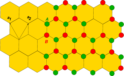
The experimental work cited in the introduction constitutes a vast evidence that the low-energy theory of electrons in graphene is described by the two-dimensional Dirac equation, which is obtained as an expansion around the Dirac points in momentum space [9, 74]. In Figure 1 we represent a finite-size ribbon of an hexagonal lattice. Two features are of importance: the first is that the lattice is not a Bravais lattice, being instead made of two inter-penetrating triangular lattices, giving rise to two geometrically nonequivalent carbon atoms, termed and ; the second is that there are two different types of edges present – zigzag and arm-chair edges. These types of edges play a different role in the physics of the ribbon. In particular, note that the zigzag edges are constituted by a single type of atom, on top and at the bottom (in the case of this figure). As is shown in Fig. 1, we can choose the direct lattice vectors to be the following:
| (4) | |||||
| (5) |
where Å is the lattice vector length. As a consequence, the reciprocal lattice vectors are
| (6) | |||||
| (7) |
The so called Dirac points in the honeycomb Brillouin zone are conveniently chosen to be
| (8) | |||||
| (9) |
If one considers only the hopping process (first nearest neighbour hopping), the tight-binding Hamiltonian is very easily written as ( is the number of unit cells in the solid)
| (10) |
where creates an electron with spin projection in the -orbital of the carbon atom of the sub-lattice , and of the unit cell ; a similar definition holds for . The exact diagonalisation of this problem is straightforward, leading to
We can expand this relation near the Dirac points, obtaining ()
| (11) |
which is a massless Dirac-like linear dispersion relation, where the velocity of light is substituted by m/s, the Fermi velocity. To obtain the effective Hamiltonian obeyed by the electrons near the Dirac points we write the matrix Hamiltonian in momentum space as
| (12) |
with given by ()
leading to the effective Hamiltonian (one valid near and the other near )
| (13) | |||||
| (14) |
with and . The Hamiltonian (13), or alternatively (14), will be the starting point of our discussion. From Eqs. (13) and (14) we can write the second-quantised Hamiltonian for electrons in graphene
| (15) |
where (for ).
Let us assume that it is possible to create a potential such that a term of the form
| (16) |
is added to the Hamiltonian (10). In terms of the formalism used to write the effective Hamiltonian (13) and (14), this term is rewritten as
| (17) |
and it corresponds to the presence of a mass term in the Hamiltonian. This type of term can be generated by covering the surface of graphene with gases molecules [75] or by depositing graphene on top of boron nitride [76, 77, 78]. The eigenvalues of are easily obtained, leading to , with , and the same for .
3 Confinement of Dirac electrons on a strip
Our goal in this section is on deriving a mathematical framework for describing the effect of confinement on Dirac electrons. The confinement can be produced either by etching, by the reduced dimensions of the graphene crystallites, or by the application of gate potentials (here the Klein tunneling poses strong limitations on the use of such method).
3.1 Boundary conditions and transverse momentum quantisation
The mathematical description of the confinement requires to impose appropriate boundary conditions to the Dirac fermions. Although, for graphene ribbons, the two types of edges discussed above impose two different types of boundary conditions [82], we shall use here the infinite mass confinement 111It is important to comment here on this particular choice for the boundary condition. Using the approach of DiVincenzo and Mele [74] one learns that , where is the bare electron mass. On the other hand, one considers that graphene electrons can not propagate in a region where the material is absent, and therefore have zero velocity there. Due to the proportionality , this can be achieved taking the limit . Therefore we could think that confinement of Dirac fermions could be achieved with a position dependent Fermi velocity , that goes to zero at the edge of the strip. Unfortunately this program does not work. Berry and Mondragon boundary boundary condition[83] corresponds to a change in the nature of the spectrum, and is somewhat artificial in what concerns graphene. The consequences of the different boundary conditions are: the properties of the wave function at graphene edges do depend on the different choices of boundary conditions, but the bulk behavior of the electronic states is essentially the same for all them; very close to the neutrality point the choice of boundary condition do again matter, but at finite doping this is not the case anymore. The choice of Berry and Mondragon boundary condition[83] does introduce a certain degree of simplicity in the calculations. proposed by Berry and Mondragon [83]. For large ribbons, there will be no important difference between the two types of boundary conditions [84], except that the infinite mass boundary condition is not able to produce edge states [85], which are present in ribbons with zigzag edges.
We shall generalise some of the results of Refs. [40, 83] by considering the case of Dirac fermions with a finite mass. The mass profile in the transverse direction () of the strip is represented in Fig. 2.
The boundary conditions the wave function has to obey, at the spatial point where the mass changes from to , are derived considering the reflection of the wave function at the boundary. Let us first consider the reflection at . The wave function in the central region () is given by
| (18) |
with ,
| (19) |
In zone (), the solution has the form
| (20) |
with
| (21) |
and
| (22) |
where the energy values are given by the same expression as that for zone . As we want to take the limit , we will assume , which implies that
| (23) |
and thus
| (24) |
where the sign in front of the square root applies to the wave function that is propagating in the positive/negative direction.. Imposing the boundary condition associated to the Dirac equation for a reflection at ,
| (25) |
one obtains
| (26) |
Taking the limit the boundary conditions reduce to
| (27) | |||||
| (28) |
Now one wants to write down the wave function of electrons propagating on the strip taking into account the confinement due to the mass term. The most general wave function is of the sum of two counter-propagating waves in the direction
| (29) |
where
| (34) |
It is always possible to redefine such that
| (39) |
a procedure that proves useful later on. Imposing the boundary conditions (28), one obtains (considering the strip to be in the range for simplicity)
| (40) |
for the relation between the coefficients, and
| (41) |
for the energy quantisation. It is clear that the admissible values of are energy dependent. Considering the limit one obtains, from Eq. (40), the simpler result , and, from Eq. (41), the condition , which leads to the transverse momentum quantisation rule [83]
| (42) |
Putting all together, the obtained results are summarised as:
| (47) |
where we have used , , and
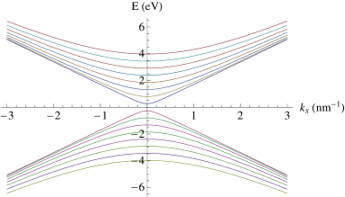
If we ignore questions of convergence, we recognise that this form for does not require or to be real. We are only assuming The dependence of the energy on shows a number of sub-bands separated by energy gaps; this is shown in Fig. (3) for a ribbon 10 nm wide. It is clear that for such a narrow ribbon one has large energy gaps between two consecutive sub-bands.
Let us represent Eq. (3.1) as , it is then simple to show that and that the normalisation coefficient reads . Note that if on the strip we have a non-zero scalar potential , we will just have to substitute by and replace by , with given by
| (48) |
3.2 Dirac fermions in a strip with a step potential
Let us now consider the scattering of Dirac fermions in a strip by a simple step potential, as represented in Fig. 4.
In the zone one has , the wave function is given by Eq. (3.1); in zone , with , the wave function is also given by Eq. (3.1) making the replacement . If, in general, the step rises up at the boundary condition takes the form
| (49) |
Solving for and gives
| (50) | |||||
| (51) |
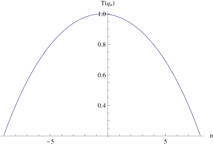
Equations (50) and (51) represent the reflection and the transmission amplitudes, respectively, for the transverse mode . It is now a simple matter to compute the tunnelling transmission for an arbitrary configuration of finite potential steps by using these two results combined with a transfer matrix method [78]. A particular case of this situation is the transmission through a potential barrier, for which is given in Fig. 5.
3.3 Trapped eigenmodes
In this section we will show that it is possible to trap massless Dirac electrons in a ribbon of finite width by creating a junction [79]. The effect exploits the fact that the spectrum of a finite ribbon exhibits energy gaps. A similar study was done in Ref. [86] for the bulk case. In this case, such a confinement is possible for certain incident angles of the eigenmodes on the potential walls [86]. The potential profile considered is shown in Fig. 6. We show that the trapping of the eigenmodes requires evanescent modes in the direction. This can be accomplished using a scalar potential.
In order to solve this problem let as again consider the case of a potential step as in Fig. 6. In region () the wave function has the form (3.1) and in region () the form would be the same with replaced by
| (52) |
One now makes the observation that if obeys the condition
| (53) |
one has a propagating wave in region and an evanescent wave in region . Within the validity of Eq. (53) it is more transparent to write the wave function in region as
| (58) |
with
| (59) |
where . Of course, the same type of analysis holds if one had considered the step at , starting at the interface between regions and . The trapping “mechanism” uses this fact. The wave function in region of Fig. 6 is taken as a sum of two counter-propagating waves along the direction, whereas in regions and only evanescent waves exists. Imposing the boundary conditions at and ( the width of the well) one obtains after a lengthy calculation the condition of the energy of the trapped eigenmodes
| (60) |
with
| (61) | |||||
and
| (62) |
Both and are pure imaginary numbers, as long as condition (53) holds true. In order to give a flavor of the numerical solution of Eq. (60) we present its numerical solution in Table 1. We have chosen the strategy of fixing the energy and looking for the values of that satisfy Eq. (60), for different values of .
-
5 59 6 65 7 78 8 113
4 Inducing mode mixing by scattering at a wall
In this section we want to discuss the scattering of Dirac electrons when they propagate along a semi-infinite narrow channel and scatterer back at the wall located at the end of the channel. This problem is intimately related to the possibility of finding a solution for the eigenmodes and eigenstates of trapped Dirac electrons in a square box. Our analysis hints at the reason why this solution has not been found yet.
4.1 Definition of the problem
Let us now consider massless Dirac fermions confined in a semi-infinite strip: and . We will look for scattering states produced by the scattering at the wall due to an incoming wave from . As before, the fermions are confined by an infinite mass term outside the strip.
The scattering state is a sum of an incoming wave, with energy , longitudinal momentum , and transverse momentum , with a superposition of all the possible outgoing channels with reflection amplitude , and it can be written as
| (69) | |||||
| (74) |
Since we are considering elastic scattering ( is an eigenstate), we must have
i.e.,
| (76) |
We must distinguish two situations:
| (77) | |||||
| (78) |
The second case corresponds to evanescent modes. We must choose this solution if we want the wavefunction to be convergent for ; for real the choice of sign reflects the fact that we have only one incoming mode. We now simplify the notation, using the fact that and are fixed, and define
| (79) | |||||
| (80) |
The parameter is just a phase, ; is also a phase for propagating modes, but for evanescent modes . For , we obtain
4.2 Calculation of the reflection coefficients
The boundary condition at the end of the semi-infinite strip and , is (see Sec. 5 for details)
| (81) |
Note that the boundary condition at an infinite-mass vertical-wall is different from that of the horizontal case discussed before. Applying the boundary condition (81) to and after rather lengthy algebra (where the replacement is made at some stage and is redefined as afterwards) one arrives at the condition
| (82) |
with given by
| (83) | |||||
The crucial step in the derivation is the observation that the set of function’s is overcomplete. In fact, the set of states with even (or with odd) is, by itself, a complete orthogonal set for functions defined in the interval . If follows that we obtain an equivalent set of conditions to Eqs. (82) by taking inner products of Eq. (82) with with even (or odd). We recall the inner products (choosing even) to be
| (84) |
The fact that the integral (84) is not a Kronecker symbol shows that, in this case, the basis is overcomplete. Using Eq. (84), we obtain
| (85) |
which is the central result of this section. This is the set of equations needed to calculate the coefficients. Naturally the convergence of the sum in (85) critically depends on the behaviour of with .
We could also have formulated the scattering problem a bit more generally, considering, for example, the case of a wave that approaches a wall at coming from . Naturally the modifications relatively to the solution found before cannot be much, given the symmetry of the problem. The first thing to note is that the boundary condition is slightly changed, being given by (see Sec. 5 for details)
| (86) |
Working out the problem along the same lines as before, one learns that the final result can be obtained from the previous solution upon the replacements
| (87) | |||||
| (88) | |||||
| (89) |
where the transformation (87) is obtained using the generator of translations, (with the momentum operator), and follows from the new position of the wall. The transformations (88) and (89) follow from the difference in the boundary condition between a right and a left vertical wall. One should note that the transformation (87) is not a phase for evanescent waves. Using transformations (87)-(89) in Eq. (83) one obtains
| (90) |
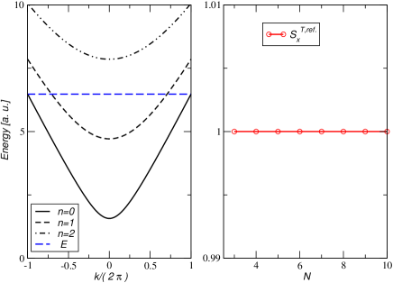
Naturally, the exact solution of the scattering problem rests upon the possibility of solving exactly the set of linear equations (85). This task seems out of reach at the moment. The second approach is to solve numerically this set of equations. This leads to the conclusion that the summation over has to be truncated at some value. To be concrete, let us consider the particular case of an incoming mode with transverse quantum number , such that the value of the incoming longitudinal momentum originates propagating modes above the mode (). Then the numerical solution of the problem has to satisfy the conservation of the probability density current (it must be one in this case) and the retained coefficients after the truncation have to converge upon increasing . As we show below, both these two conditions are satisfied for small . For the numerical solution we choose , , such that the value of leads to and as the only two propagating modes. We use a set of units such that and . Further we take which implies that , since the scattering being elastic can not excite hole states, which have . The equations to be solved numerically are given in A.
The probability density current transported by the mode is defined as
| (91) |
Since the motion is transversely confined, what is needed is the probability density current along the -direction, which reads
| (92) |
Using definition (92), the total reflected flux density, , obeys the sum rule
| (93) |
with
| (94) |
with both and real. In agreement with our expectations, the sum-rule is better fulfilled the larger is, although modest values of do a good job as well. In fact, in the right panel of Fig. 7 one can see that the sum rule is fulfilled even considering only one evanescent mode ().
In Fig. 8 we study, for the particular mode occupation defined in the left panel of Fig. 7, the evolution of the coefficients as function of . We write each coefficient as . In Fig. 8, we plot the square of the modulus of (left panels) and the corresponding phase (right panels), separating the cases for which (propagating modes), which are represented in the two top panels, from those where (evanescent modes), which we represent in the two bottom panels.
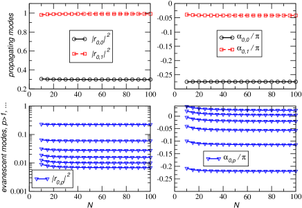
A beautiful result emerges from this study. The wall introduces mode mixing and generates evanescent waves, whose contribution to the total wave function diminuishes upon increasing . This result is quite different from that for Schrödinger electrons, where no mode mixing takes place. The fundamental reason is due to the fact that for Schrödinger electrons the transverse wave-function is the same for the incoming and outgoing waves. For Dirac electrons, on the contrary, the spinor of the incoming and outgoing waves change due to its dependence on either the incoming or outgoing momentum.
Had we tried to force the solution of the problem using only one incoming and one outgoing propagating modes, with the same value, and we would have obtained the trivial solution . This statement is easily proved as follows: we make the assumption that the total wave function should be a sum of two terms of the form
| (101) | |||||
| (106) |
where the phase-shift was introduced. Let us now impose the boundary condition (81) on the wave function (LABEL:eq:scattering_specialcase). Working out the calculation, one obtains two conditions that must be fulfilled simultaneously
| (108) |
with defined from . It is clear that the two conditions in Eq. (108) cannot be satisfied, in general, at the same time, which precludes the proposal of Eq. (LABEL:eq:scattering_specialcase) as a solution to the problem. In fact, the two conditions given by Eq. (108) are equivalent to
| (109) |
which can only be true if , a situation that occurs only if
| (110) |
which finally is true only in the trivial case . This means that the wave function has no dependence and that the electronic density is , constant everywhere (for finite the density does show oscillations inside the box [80]). The exact solution of the square billiard with infinite-mass confinement is therefore a quite elusive problem [83].
5 Confinement of Dirac fermions in quantum dots
Let us now consider the confinement of Dirac fermions in quantum dots. Naively one would expect that the rectangular dot would have a simple solution (as it has in the Schrödinger case), since the wave function of the confined Dirac electrons (by an infinite mass term) in a strip can be written in terms of elementary trigonometric functions. In fact this is not the case. The only known case so far of an integrable Dirac dot (billiard), subjected to the infinite mass confinement, is the circular one. In order to solve this problem one needs the boundary condition obeyed by the wave function at the dot boundary. This was worked out by Berry and Mondragon [83] and the geometry they used is represented in Fig. 9. They considered a quantum dot represented by a domain of arbitrary shape, separated by an outside region that we denominate . The boundary of the domain is parametrised by an length arc , where the vector normal to the surface of the dot at is given by
| (111) |
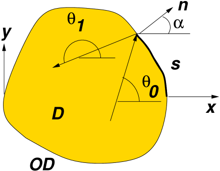
Imposing the condition of zero flux perpendicular to the wall of the dot one obtains
| (112) |
The constant is determined working out the study of a reflecting wave at the boundary of the dot, when the mass in the region obeys the condition . The final result is [83], and the detailed calculation can be found in B.
5.1 The circular dot with zero magnetic field
Let us first write the free solutions of the Dirac equation in polar coordinates and . In this coordinates the Dirac Hamiltonian and the wave function read [87, 88, 89, 90, 91]
| (115) |
and
| (118) |
respectively, where is the Bessel function of integer order . A detailed derivation of these results is given in C. In order to obtain the eigenvalues of the electrons in the dot one has to apply the boundary condition (112). Note that because one has a circular dot . This latter property makes it possible to satisfy the boundary condition (112) with the wave function (118) alone. In fact, for a dot of radius , one has
| (119) |
whose numerical solution gives the value of for a given and , and from this the energy levels are computed using . The eigenvalues are defined by three quantum numbers: , , and , where represents the ascending order of the values of that satisfy (119), for a given and . In the next section we give numerical results for the energy eigenvalues.
5.2 The circular dot in a finite magnetic field
Let us now see how we can adapt our formalism to address the calculation of the energy eigenvalues of a circular dot in a magnetic field, that is we want to study the formation of Landau levels in reduced geometries (amusing enough, the first calculation of Landau levels using the Dirac equation is as old as quantum mechanics itself [92], a result that was forgotten by the graphene community). Experimentally this situation has been realised in Ref. [93]. The cyclotron motion of bulk graphene was discussed in Ref. [94].
The Hamiltonian (115) was written for a single Dirac cone. As is shown in C, the Hamiltonian for the two Dirac cones can be written using an additional quantum number , associated with the valley index, reading
| (120) |
In this section we do not use the infinite mass boundary condition, but introduce the zigzag type of boundary condition. This will allow us to consider the presence edge states [95]. As we will show in the next section, these states are always present in graphene quantum dots. Recalling Fig. 1, one sees that at the zigzag edge only one type of carbon atom (either or ) is present. The boundary condition at a zigzag edge with, say, only atoms present, requires that the amplitude of the wave function at the atoms to be zero, we therefore have the condition
| (121) |
In the following we will choose the boundary condition defined by Eq. (121), for which the wave vector is quantised as , where denotes the -th root of the -th Bessel function, .
A magnetic field , perpendicular to the graphene sheet, gives rise to a vector potential, which in polar coordinates reads , and, using Gauss’ theorem, one obtains . Making the traditional minimal coupling of the charged electrons to the vector potential, the Hamiltonian has the form
| (122) |
where Tnm2 denotes the elementary flux quantum and is the electron charge. We now make the observation that the trial function
| (123) |
renders the eigenvalue problem a one-dimensional one, with the radial Hamiltonian given by
| (124) |
Let us make the substitution () in the eigenvalue equation defined by the Hamiltonian (124), with the radial spinor wave function having the form . This substitution was considered before in the exact solution of the Coulomb problem in the 2+1 dimensional Dirac equation [96] and also in [89]. This procedure leads to a more symmetric eigenproblem of the form
| (125) | |||||
| (126) |
We want to solve the eigenproblem defined by (125) and (126) by diagonalising an Hermitian matrix.
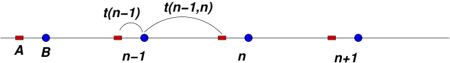
To this end let us look at the problem of a dimerised one-dimensional tight-binding model, such as that represented in Fig. 10. The relevance of this interlude will be apparent in a moment. The Hamiltonian for the depicted system is
| (127) |
and the wave function is written as
| (128) |
The eigenvalue equation can be reduced to the solution of the linear homogeneous system
| (129) | |||
| (130) |
Introducing the simplifying notation , the above eigensystem reads
| (131) | |||||
| (132) |
We note that Eqs. (131) and (132) pose well defined numerical problem for well behaved functions and . Let us now see what kind of continuous model follows from this lattice problem. Notice that since the model under consideration has a valence and a conduction bands, in case we have one electron per site the relevant energies are around zero. In this case, the amplitudes and oscillate between positive and negative values within a lattice unit cell. In order to construct a well defined continuous model we need to subtract this oscillatory behaviour making the replacement and . This produces the set of equations
| (133) | |||||
| (134) |
Defining now and and recalling that the first order derivatives can be approximated by
| (135) | |||
| (136) |
and that , a discretised position vector, with the length of the chain (which will correspond latter to the radius of the dot), , and the number of points in which the length was discretised, we obtain
| (137) | |||||
| (138) |
We can thus make the following identification to the continuous model:
| (139) | |||||
| (140) |
The ambiguity introduced by the sign in Eq. (140) can be settled by looking at the bulk limit of the problem. The choice that gives the correct answer is and . If we assume that the wall of the dot is located at , then the boundary condition (121) is imposed considering . In order to keep the problem particle-hole symmetric, we consider the case where the effective chain problem has unit cells.
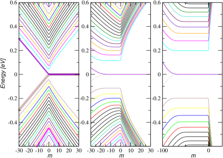
In Fig. 11 we represent the numerical solution of Eqs. (131) and (132). It is clear that at small fields the bands are essentially symmetric for positive and negative values, a property that comes from the fact that exchanging by in the Dirac equation only replaces the role of and . With a finite magnetic field the situation changes. Also seen is the presence of a dispersive edge state. The dispersive part, occurring for positive , is dependent on the Dirac point. Note the appearance of the zero energy Landau level upon increasing the magnetic field. The different behaviour, for large fields, shown by the energy levels for positive and negative is associated to the amount of angular momentum induced by the magnetic field.
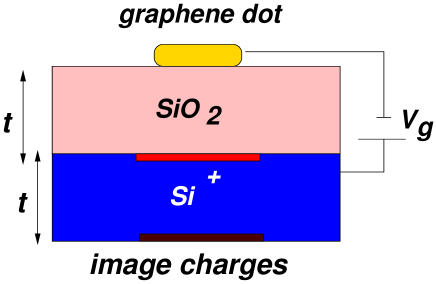
Let us now discuss how to include the Coulomb interaction in the calculation. This is important because the screening in the dot may not be very effective and because the dot may be working under a regime where it has a net charge density (charged dot). The situation of a charged dot is represented in Fig. 12. The gate potential induces either holes or electrons in the dot. This causes a situation where the dot is charged, since the neutrality case takes place when the chemical potential is at the Dirac point. If we take the graphene to be at a potential then the charges accumulated in the metal-insulator interface have to be at zero potential. This means that one must use a set of images charges at a distance from the interface with exactly the same spatial density of that formed in the graphene dot. We then have to describe the Coulomb interaction of an electron in the dot with both the self-consistent charge density in the graphene and its image underneath the metal-insulator interface [100].
The simplest way to include the effect of Coulomb repulsion is by using the self-consistent Hartree approximation. We analyse here the effects induced by increasing the number of electrons in the dot using the Hartree approximation [97]. The self-consistent Hartree potential describes, within a mean field approximation, the screening of charges within the dot. We assume that a half-filled dot is neutral, as the ionic charge compensates the electronic charge in the filled valence band. Away from half filling, the dot is charged. Then, an electrostatic potential is induced in its interior, and there is an inhomogeneous distribution of charge. We describe charged dots by fixing the chemical potential, and obtaining a self-consistent solution where all electronic states with lower energies than the Fermi energy are filled. From this calculation we obtain the Hartree electronic energy bands. The Hartree approximation should give a reasonable description when Coulomb blockade effects can be described as a rigid shift of the electrostatic potential within the dot [98, 99]. Using the same discretisation procedure as before, the numerical equations to be solved have now the form
| (141) | |||||
| (142) |
where the Hartree potential in the continuum, , is given by
| (143) |
and
| (144) |
with the parameter given by and the electronic density at point , computed from
| (145) |
such that the sums over and are constrained to those energy levels such that (note that the explicit dependence of and on and has been introduced in Eq. 145), where is the Fermi energy measured relatively to the Dirac point, is the spin and valley degeneracy, and the constant is given by the normalisation condition on the disk, . The constraint in the summation in Eq. (145) is due to the fact that the boundary conditions introduced by the finite tight-binding chain fails to reproduce accurately the boundary condition , introducing a spurious mode, characterised by the quantum number for ; in order for sensible results to be obtained these modes have to be removed.
We note that the integral (143) is well behaved since the self-interaction has been excluded (). Further the is independent of . The angular integral in Eq. (143) can be formally computed leading to
| (146) | |||||
with defined as
| (147) |
The elliptic integral can be approximated by an analytical function [101], which reduces the numerical effort. It is now clear that, due to the Hartree potential, the problem defined by Eqs. (141) and (142) has to be solved self-consistently.
One should comment on the fact that for a large dot the contribution from essentially vanishes and the change of the bands due to the Hartree term is vanishingly small. On the contrary, for small dots and the Hartree renormalisation of the electronic energy levels can be very important in the case of heavily charged dots.
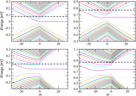
In Fig. 13 we represent the energy bands of a quantum dot of radius nm on top of a silicon oxide slab of thickness nm. We used a gate voltage of V, which corresponds to a Fermi energy of eV for the bulk system, The values of the magnetic field used were T (top panels) and T (bottom panels). It is clear that the Hartree bands are renormalised by the Coulomb interaction.
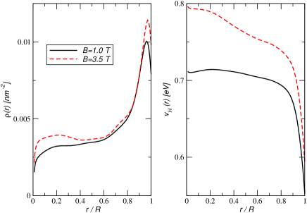
In Fig. 14 we represent the self-consistent density, , and Hartree potential, , for two different values of the magnetic field. The parameters are those given in the caption of Fig. 13. The increase in the Hartree potential upon increasing is due to the increase of the number of electrons in the dot.
We should comment that in our calculation we have not tried to keep the number of electrons fixed. This can easily be done, but increases the computational effort since the chemical potential has to be self-consistently determined. Instead, we have chosen to keep the Fermi energy constant, which, of course, leads to a changing in the number of electrons in the dot with the variation of the magnetic field. Also the population of the surface states was not included in the calculation, using a criterion of computational simplicity. In a future study we shall relax these two constraints.
Another important aspect in quantum dot physics is that of confinement introduced by the potential creating the dot. The confinement potential can be either due to etching or to applied gates. In the case of dots or narrow channels described by the Schrödinger equation, a very popular confinement is that introduced by a parabolic potential [102], since it allows a simple analytical solution. We choose a confinement potential given by
| (148) |
which rises smoothly from the centre of the dot. The prefactor is the strength of the potential at the edge of the dot. As in the case of the Hartree potential, enters in the diagonal part of the radial Hamiltonian. In Fig. 15 we give a comparison of the energy bands for T. Comparing the left and the right panels of Fig. 15 we see that the Landau levels become dispersive with due to the confinement, a result also found for Landau levels derived from the Schrödinger equation [102]. Interestingly, we see that the confinement also breaks the particle-hole symmetry of the problem, a result found before for the ribbon problem [103].
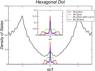
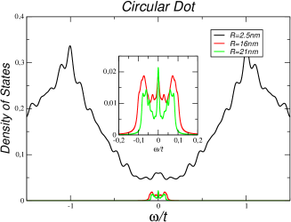
5.3 The hexagonal and circular dots at the tight-binding level
In this subsection we want to address the question whether graphene quantum dots will have or not edge states, starting from the full solution of the tight-binding Hamiltonian (10). Edge states in graphene nanostructures are of particular importance since they can give rise to magnetism see, e.g., Ref. [104]. In order to access the low energy density of states of dots with physically relevant sizes (bigger than 10 nm) a Lanczos technique is used, since the exact diagonalisation of systems of this size becomes intractable. For a brief introduction to the Lanczos technique, see e.g. Ref. [105].
We have chosen to diagonalise dots of circular and shape with zigzag-termination, such as those depicted in Fig. 16.

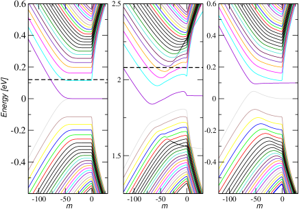
Our numerical findings are represented in the Fig. 17. It is clear that as the size of the dot grows larger the number of zero energy states increases, indicating the presence of zero energy-edge states. When a finite is added to the Hamiltonian, the edge states become dispersive [39] and there is a reduction of the density of zero energy states (seen in the hexagonal dot).
6 Final comments
In this work a description of the confinement of Dirac electrons in nano-wires and quantum dots was given. It was shown that, in principle, it is possible to localise electronic modes in a spatial region of a nanowire, using a gate potential setup. The energy spectrum of quantum dots in a magnetic field was described taking into account both the effect of electron-electron interactions, at the Hartree level, and the effect of confining potentials. The inclusion of exchange [106, 107, 108] in this study can in principle be done. The interesting aspects about this possibility are two-fold: first, the exchange energy for Dirac electrons is different from that for the two-dimensional electron gas described by the Schrödinger equation; second, and contrary to the Hartree potential, the exchange energy of the full electronic system has to be considered, since there is not an equivalent cancellation effect to that found in the Hartree potential between the ion background and the valence electrons direct Coulomb energy. These aspects will be pursued in a follow-up study [109].
Appendix A Equations for the numerical solution of the scattering problem
Below we give the equations that have been solve numerically when we studied the scattering problem by a infinite-mass wall. These are:
-
•
:
-
•
and even:
with the possibility of having in the summation
-
•
odd
with the possibility of having in the summation. It is clear that we can truncate this set of equations to obtain a set of equations for the coefficients .
Appendix B General boundary conditions in a quantum dot with infinite mass confinement
In this Appendix we give all the details of how to obtain the boundary condition of the wave function at the wall of a quantum dot, with the confinement determined by the infinite mass condition. We must compute the wave function in the domain due to a reflection at the boundary. We write the plane-wave inside as
| (152) |
where from Fig. 9 we can conclude that , and and are the momenta of the incident and reflected waves at the boundary of the dot. In order to calculate (which will make it possible to compute the value of ), we need to discover the value of the reflection coefficient, . We can accomplish this, using the fact required by the Dirac equation, that the components of the spinors must be continuous at the boundary.
First we solve the Dirac equation with a mass . For the sake of simplicity, we use the normal and tangential coordinates and given by
which implies that,
resulting in
Then, for a plane wave in the domain (complementary to ), , (where stands for the transmission coefficient). Solving the Dirac equation explicitly we obtain
| (155) |
where we have defined
and chosen the solution that decays for . Further we identified and . Imposing the continuity of the wave functions (152) and (155) at the boundary of the dot, one obtains
Replacing the value of in Eq. (152), the wave function in the dot reads
| (160) |
which, after some simple manipulations, allows us to conclude that
and therefore .
Appendix C The Dirac equation in polar coordinates
To treat problems with circular symmetry, the partial derivatives with respect to Cartesian coordinates shall be written in polar coordinates (). For the -coordinate, the product rule yields , where the derivatives are taken for fixed . The first derivative is obtained using . The second one uses and thus . This gives
| (161) |
and analogously
| (162) |
The Hamiltonian thus reads
| (163) |
where we have introduced the additional quantum number , to account for the two non-equivalent Dirac points. Let us now define the operators
| (164) | |||||
| (165) |
which acting on the product of a Bessel function of integer order , , and a complex exponential, , produce . This last result leads to the construction of the wave function of the free problem in the form given in Eq. (118). In addition, the following commutators and allow us to interpret the operators as rising and lowering operators of the angular momentum.
Finally we note that if we consider a ring instead of a disk it is possible to add a flux through the ring, introducing a vector potential . The full Hamiltonian with both a perpendicular magnetic field and the magnetic flux through the ring is given by
| (166) |
and its numerical solution can be accommodated within the explained method.
References
References
- [1] K. S. Novoselov, A. K. Geim, S. V. Morozov, D. Jiang, Y. Zhang, S. V. Dubonos, I. V. Grigorieva, and A. A. Firsov, Science 306, 666 (2004).
- [2] K. S. Novoselov, D. Jiang, T. Booth, V.V. Khotkevich, S. M. Morozov, A. K. Geim, PNAS 102, 10451 (2005).
- [3] Chuhei Oshima and Ayato Nagashima, J. Phys.: Condens. Matter 9, 1 (1997).
- [4] A. H. Castro Neto, F. Guinea, N. M. R. Peres, Physics World, 11, 33 (2006).
- [5] A. K. Geim and K. S. Novoselov, Nature Materials 6, 183 (2007).
- [6] M. I. Katsnelson, Materials Today 10, 20 (2007).
- [7] A. K. Geim and A. H. MacDonald, Physics Today 60, 35 (2007).
- [8] A. K. Geim and P. Kim, Scientific American, April, 90 (2008).
- [9] A. H. Castro Neto, F. Guinea, N. M. R. Peres, K. S. Novoselov, and A. K. Geim, to be published in Review of Modern Physics, arXiv:0709.1163v2.
- [10] C. W. Beenakker, to be published in Review of Modern Physics, arXiv:0710.3848v2.
- [11] Tim J. Booth, Peter Blake, Rahul R. Nair, Da Jiang, Ernie W. Hill, Ursel Bangert, Andrew Bleloch, Mhairi Gass, Kostya S. Novoselov, M. I. Katsnelson, and A. K. Geim, Nano Lett. 8, 2442 (2008).
- [12] Yenny Hernandez, Valeria Nicolosi, Mustafa Lotya1, Fiona M. Blighe1, Zhenyu Sun, Sukanta De1, I. T. McGovern, Brendan Holland, Michele Byrne, Yurii K. Gun’Ko, John J. Boland, Peter Niraj, Georg Duesberg, Satheesh Krishnamurthy, Robbie Goodhue, John Hutchison, Vittorio Scardaci, Andrea C. Ferrari, and Jonathan N. Coleman, Nature Nanotechnology , (2008).
- [13] Xiaolin Li, Guangyu Zhang, Xuedong Bai, Xiaoming Sun, Xinran Wang, Enge Wang, and Hongjie Dai, Nature Nanotechnology , (2008).
- [14] S. Yoshimura and R. P. H. Chang, editors, Supercarbon: Synthesis, Properties and Applications, (Berlin: Springer, 1998).
- [15] D. D. L. Chung, J. Mater. Sci. 37, 1 (2002).
- [16] J. E. Field, editor, Properties of Natural and Synthetic Diamond, (San Diego: Academic Press, 1992).
- [17] Andreas Barth and Werner Marx, arXiv:0808.3320.
- [18] Changgu Lee, Xiaoding Wei, Jeffrey W. Kysar, and James Honel, Science 321, 385 (2008).
- [19] A. A. Balandin, S. Ghosh, W. Bao, I. Calizo, D. Teweldebrhan, F. Miao, C. N. Lau, Nano Lett. 8, 902 (2008).
- [20] J. Scott Bunch, Scott S. Verbridge, Jonathan S. Alden, Arend M. van der Zande, Jeevak M. Parpia, Harold G. Craighead, and Paul L. McEuen, arXiv:0805.3309v1.
- [21] S.V. Morozov, K.S. Novoselov, M.I. Katsnelson, F. Schedin, D.C. Elias, J.A. Jaszczak, and A.K. Geim, Phys. Rev. Lett. 100, 016602 (2008).
- [22] K. I. Bolotin, K. J. Sikes, Z. Jiang, M. Klima, G. Fudenberg, J. Hone, P. Kim, and H. L. Stormer, Sol. Stat. Comm. 146, 351 (2008).
- [23] N. M. R. Peres, F. Guinea, and A. H. Castro Neto, Phys. Rev. B 73, 195411 (2006); Phys. Rev. B 73, 239902 (2006).
- [24] Yu-Ming Lin, Vasili Perebeinos, Zhihong Chen, and Phaedon Avouris, arXiv:0805.0035v2.
- [25] Anton Sidorov, David Mudd, Gamini Sumanasekera, P. J. Ouseph, C. S. Jayanthi, and Shi-Yu Wu, arXiv:0808.1577v1.
- [26] Taisuke Ohta,Aaron Bostwick, Thomas Seyller, Karsten Horn, and Eli Rotenberg1, Science 313, 951 (2006).
- [27] M. Mucha-Kruczyński, O. Tsyplyatyev, A. Grishin, E. McCann, Vladimir I. Fal’ko, Aaron Bostwick, and Eli Rotenberg, Phys. Rev. B 77, 195403 (2008).
- [28] S. Y. Zhou, G.-H. Gweon, A. V. Fedorov, P. N. First, W. A. de Heer, D.-H. Lee, F. Guinea, A. H. Castro Neto, and A. Lanzara, Nature Materials 6, 770 (2007)
- [29] S.Y. Zhou, D.A. Siegel, A.V. Fedorov, F.El Gabaly, A.K. Schmid, A.H. Castro Neto, D.-H. Lee, and A. Lanzara, Nature Materials 7, 259 (2008).
- [30] R. S. Deacon, K-C. Cdhuang, R. J. Nicholas, K. S. Novoselov, and A. K. Geim, Phys. Rev. B 76, 081406(R) (2007).
- [31] N. M. R. Peres, J. M. B. Lopes dos Santos, and T. Stauber, Phys. Rev. B 76, 073412 (2007)
- [32] T. Stauber, N. M. R. Peres, and F. Guinea, Phys. Rev. B 76, 205423 (2007)
- [33] Tomas Lofwander and Mikael Fogelstrom, Phys. Rev. B 76, 193401 (2007)
- [34] Maxim Trushin and John Schliemann, Phys. Rev. Lett. 99, 216602 (2007)
- [35] Xu Du, Ivan Skachko, Anthony Barker, and Eva Y. Andrei, Nature Nanotechnology 3, 491 (2008).
- [36] S. Adam and S. Das Sarma, Sol. Stat. Comm. 146, 356 (2008).
- [37] T. Stauber, N. M. R. Peres, and A. H. Castro Neto, Phys. Rev. B 78, 085418 (2008).
- [38] Jessica L. McChesney, Aaron Bostwick, Taisuke Ohta, Konstantin Emtsev, Thomas Seyller, Karsten Horn, and Eli Rotenberg, arXiv:0809.4046.
- [39] N. M. R. Peres, F. Guinea, A. H. Castro Neto, Phys. Rev. B 73, 125411 (2006).
- [40] J. Tworzydlo, B. Trauzettel, M. Titov, A. Rycerz, and C.W.J. Beenakker Phys. Rev. Lett. 96, 246802 (2006).
- [41] M. I. Katsnelson, Eur. Phys. J. B 51, 157 (2006).
- [42] K. Ziegler, Phys. Rev. B 75, 233407 (2007).
- [43] F. Miao, S. Wijeratne, Y. Zhang, U. C. Coskun, W. Bao, and C. N. Lau, Science 317, 1530 (2007).
- [44] R. Danneau, F. Wu, M.F. Craciun, S. Russo, M.Y. Tomi, J. Salmilehto, A.F. Morpurgo, and P.J. Hakonen, Phys. Rev. Lett. 100, 196802 (2008).
- [45] W. E. Hill, A. K. Geim, K. Novoselov, F. Schedin, P. Blake, IEEE Transactions on Magnetics, 42, 2694 (2006).
- [46] Sungjae Cho, Yung-Fu Chen, and Michael S. Fuhrer, Appl. Phys. Lett. 91, 123105 (2007).
- [47] Nikolaos Tombros, Csaba Jozsa, Mihaita Popinciuc, Harry T. Jonkman, and Bart J. van Wees, Nature 448, 571 (2007).
- [48] C. Jozsa, M. Popinciuc, N. Tombros, H. T. Jonkman, and B. J. van Wees, arXiv:0802.2628v2.
- [49] Z. Q. Li, E. A. Henriksen, Z. Jiang, Z. Hao, M. C. Martin, P. Kim, H. L. Stormer, and D. N. Basov, Nature Physics 4, 532 (2008).
- [50] Z. Q. Li, E. A. Henriksen, Z. Jiang, Z. Hao, M. C. Martin, P. Kim, H. L. Stormer, and D. N. Basov, arXiv:0807.3776v1.
- [51] V. P. Gusynin, S. G. Sharapov, and J. P. Carbotte, Int. Jour. Mod. Phys. B 21, 4611 (2007).
- [52] T. Stauber, N. M. R. Peres, and A. H. Castro Neto, Phys. Rev.B 78, 085418 (2008).
- [53] R. R. Nair, P. Blake, A. N. Grigorenko, K. S. Novoselov, T. J. Booth, T. Stauber, N. M. R. Peres, and A. K. Geim, Science 320, 1308 (2008).
- [54] T. Stauber, N. M. R. Peres, and A. K. Geim, Phys. Rev. B 78, 085432 (2008).
- [55] Johan Nilsson, A. H. Castro Neto, F. Guinea, and N. M. R. Peres, Phys. Rev. Lett. 97, 266801 (2006); Phys. Rev. B 78, 045405 (2008).
- [56] D. S. L. Abergel and Vladimir I. Fal’ko, Phys. Rev. B 75, 155430 (2007).
- [57] E. J. Nicol and J. P. Carbotte, Phys. Rev. B 77, 155409 (2008).
- [58] Xuan Wang, Linjie Zhi, and Klaus Müllen, Nano Lett. 8, 323 (2008).
- [59] Junbo Wu, Héctor A. Becerril, Zhenan Bao, Zunfeng Liu, Yongsheng Chen, and Peter Peumans, Appl. Phys. Lett. 92, 263302 (2008).
- [60] P. Blake, P. D. Brimicombe, R. R. Nair, T. J. Booth, D. Jiang, F. Schedin, L. A. Ponomarenko, S. V. Morozov, H. F. Gleeson, E. W. Hill, A. K. Geim, and K. S. Novoselov, Nano Lett., 8 , 1704 (2008).
- [61] A. B. Kuzmenko, E. van Heumen, F. Carbone, and D. van der Marel, Phys. Rev. Lett. 100, 117401 (2008).
- [62] F. Schedin, A. K. Geim, S. V. Morozov, D. Jiang, E. H. Hill, P. Blake, and K. S. Novoselov, Nature Materials 6, 652 (2007).
- [63] Jannik C. Meyer, C. O. Girit1, M. F. Crommie, and A. Zettl, Nature 454, 319 (2008).
- [64] Marcus Freitag, Nature Nanotechnology 3, 455 (2008)
- [65] Xiaolin Li, Xinran Wang, Li Zhang, Sangwon Lee, and Hongjie Dai, Science 319, 1229 (2008).
- [66] L. A. Ponomarenko, F. Schedin, M. I. Katsnelson, R. Yang, E. W. Hill, K. S. Novoselov, and A. K. Geim, Science 320, 356 (2008).
- [67] C. Stampfer, J. Güttinger, F. Molitor, D. Graf, T. Ihn, and K. Ensslin, Appl. Phys. Lett. 92, 012102 (2008).
- [68] C. Stampfer, E. Schurtenberger, F. Molitor, J. Güttinger, T. Ihn, and K. Ensslin, Nano Lett. 8, 2378 (2008).
- [69] P. G. Silvestrov and K. B. Efetov, Phys. Rev. Lett. 98, 016802 (2007).
- [70] F. Sols, F. Guinea, and A. H. Castro Neto, Phys. Rev. Lett. 99, 166803 (2007).
- [71] B. Wunsch, T. Stauber, F. Sols, and F. Guinea, Phys. Rev. Lett. 101, 036803 (2008).
- [72] M. I. Katsnelson and F. Guinea, Phys. Rev. B 78, 075417 (2008).
- [73] Xinran Wang, Yijian Ouyang, Xiaolin Li, Hailiang Wang, Jing Guo, and Hongjie Dai, Phys. Rev. Lett. 100, 206803 (2008).
- [74] D. P. DiVincenzo and E. J. Mele, Phys. Rev. B 29, 1685 (1984).
- [75] R. M. Ribeiro, N. M. R. Peres, J. Coutinho, and P. R. Briddon, Phys. Rev. B 78, 075442 (2008).
- [76] Gianluca Giovannetti, Petr A. Khomyakov, Geert Brocks, Paul J. Kelly, and Jeroen van den Brink, Phys. Rev. B 76, 73103 (2007).
- [77] Y. H. Lu, P. M. He, and Y. P. Feng, arXiv:0712.4008.
- [78] J. Viana Gomes and N. M. R. Peres, J. Phys.: Cond. Matt. 20, 325221 (2008)
- [79] Vadim V. Cheianov and Vladimir I. Fal’ko, Phys. Rev. B 74, 041403 (2006).
- [80] P. Alberto, C. Fiolhais, and V. M. S. Gil, Eur. J. Phys. 17, 19 (1996).
- [81] M. M. Fogler, L. I. Glazman, D. S. Novikov, B. I. Shklovskii, Phys. Rev. B 77, 075420 (2008).
- [82] L. Brey and H.A. Fertig, Phys. Rev. B 73, 235411 (2006).
- [83] M. V. Berry and R. J. Mondragon, Proc. R. Soc. Lond. A 412, 53 (1987).
- [84] A. R. Akhmerov and C. W. J. Beenakker, Phys. Rev. B 77, 085423 (2008).
- [85] Eduardo V. Castro, N. M. R. Peres, J. M. B. Lopes dos Santos, A. H. Castro Neto, and F. Guinea, Phys. Rev. Lett. 100, 026802 (2008).
- [86] L. Zhao and S. F. Yelin, cond-mat.other/0804.2225v1.
- [87] Martina Hentschel and Francisco Guinea, Phys. Rev. B 76, 115407 (2007)
- [88] P. Recher, B. Trauzettel, A. Rycerz, Ya. M. Blanter, C. W. J. Beenakker, and A. F. Morpurgo, Phys. Rev. B 76, 235404 (2007).
- [89] B. Wunsch, T. Stauber, and F. Guinea, Phys. Rev. B 77, 035316 (2008).
- [90] Jozsef Cserti, Andras Palyi, and Csaba Peterfalvi, Phys. Rev. Lett. 99, 246801 (2007).
- [91] Prabath Hewageegana and Vadym Apalkov, Phys. Rev. B 77, 245426 (2008).
- [92] I. I. Rabi, Z. Phys. 49, 507 (1928).
- [93] C. Stampfer, S. Schnez, J. Guettinger, S. Hellmueller, F. Molitor, I. Shorubalko, T. Ihn, and K. Ensslin, arXiv:0807.2710v1.
- [94] John Schliemann, New J. Phys. 10, 043024 (2008).
- [95] K. Wakabayashi, M. Fujita, H. Ajiki, and M. Sigrist, Phys. Rev. B 59, 8271 (1999).
- [96] Shi-Hai Dong and Zhong-Qi Ma, Phys. Lett. A 312, 78 (2003).
- [97] K. L. Janssens, B. Partoens, and F. M. Peeters, Phys. Rev. B 64, 155324 (2001).
- [98] D. V. Averin and K. K. Likharev, in B. L. Altshuler, P. A. Lee, and R. A. Webb, editors, Mesoscopic Phenomena in Solids, (Amsterdam: Elsevier, 1991).
- [99] H. Grabert and M. H. Devoret, editors, Single Electron Tunneling, (New York: Plenum, 1992).
- [100] J. Ferńandez-Rossier, J. J. Palacios, and L. Brey, Phys. Rev. B 75, 205441 (2007).
- [101] Milton Abramowitz and I. A. Stegun, Handbook of Mathematical Functions, (New York: Dover, 1965).
- [102] K.-F. Berggren, G. Roos, and H. van Houten, Phys. Rev. B 37, 10118 (1988).
- [103] N. M. R. Peres, A. H. Castro Neto, and F. Guinea, Phys. Rev. B 73, 241403 (2006).
- [104] Somnath Bhowmick and Vijay B. Shenoy, J. Chem. Phys. 128, 244717(2008).
- [105] T. D. Kühner and S. R. White, Phys. Rev. B 60, 335 (1999).
- [106] N. M. Peres, F. Guinea, and A. H. Castro Neto, Phys. Rev. B 72, 174406 (2005).
- [107] Johan Nilsson, A. H. Castro Neto, N. M. Peres, and F. Guinea, Phys. Rev. B 73, 214418 (2006).
- [108] M. W. C. Dharma-wardana, Phys. Rev. B 75, 075427 (2007).
- [109] N. M. R. Peres and T. Stauber, in preparation.