]Electronic address: mario.silveirinha@co.it.pt
Superlens made of a metamaterial with extreme effective parameters
Abstract
We propose a superlens formed by an ultra-dense array of crossed metallic wires. It is demonstrated that due to the anomalous interaction between crossed wires, the structured substrate is characterized by an anomalously high index of refraction and supports strongly confined guided modes with very short propagation wavelengths. It is theoretically proven that a planar slab of such structured material makes a superlens that may compensate for the attenuation introduced by free-space propagation and restore the subwavelength details of the source. The bandwidth of the proposed device can be quite significant since the response of the structured substrate is non-resonant. The theoretical results are fully supported by numerical simulations.
pacs:
42.70.Qs, 78.20.Ci, 41.20.Jb, 78.66.SqI Introduction
The resolution of classical imaging systems is limited by Rayleigh’s diffraction limit, which establishes that the width of the beam spot at the image plane cannot be smaller than . The subwavelength details of an image are associated with evanescent spatial harmonics which exhibit an exponential decay in free-space. Classical imaging systems only operate with propagating spatial harmonics, and due to this reason the subwavelength information is irremediably lost.
In recent years, there has been a great interest in approaches that may allow overcoming the classical diffraction limit and enable subwavelength imaging Pendry (2000); Taubner et al. (2006); Fang et al. (2005); Freire and Marques (2005); Belov et al. (2006); Salandrino and Engheta (2006); Liu et al. (2007); Smolyaninov et al. (2007); Merlin (2007). In particular the “perfect lens” introduced in Pendry (2000) has received significant attention, due to its promise of perfect imaging. The superlens is formed by a thin slab of a material with either negative permittivity Taubner et al. (2006); Fang et al. (2005) or negative permeability Freire and Marques (2005), or both. The mechanism used by the superlens to restore the evanescent spatial spectrum is based on the resonant excitation of surface waves. In this work, we explore an alternative approach to obtain imaging with subwavelength resolution that does not require materials with negative effective parameters. In our recent work Silveirinha and Fernandes (2008), it was shown that a structured material formed by an array of crossed metallic wires (see Fig. 1) has very peculiar properties, and is characterized by an anomalously high positive index of refraction. This property is quite surprising since intuitively one might expect that in the long wavelength limit the material would not support propagating plane waves, and instead would have plasma-like properties. It was demonstrated in Silveirinha and Fernandes (2008), that in reality the material is not characterized by a negative permittivity, but quite differently it may interact with electromagnetic waves as a material with very large positive permittivity. In particular, a slab of the considered material may support ultra-subwavelength guided modes with very short guided wavelengths Silveirinha and Fernandes (2008). These exciting properties have been experimentally verified at microwaves in Silveirinha et al. (accepted for publication in Appl. Phys. Lett.). Here, we will demonstrate that the resonant excitation of guided modes may enable a “superlensing” effect somehow analogous to the effect obtained using a silver lens Pendry (2000); Fang et al. (2005).
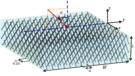
It is important to mention that arrays of parallel metallic wires have been used before to achieve sub-diffraction imaging Belov et al. (2006, 2008). However, in these previous works the imaging mechanism was based on the conversion of evanescent waves into transmission line modes, and did not involve the excitation of guided modes or the enhancement of evanescent waves. Due to this reason, in Belov et al. (2006, 2008) the source must be placed in the immediate vicinity of the imaging device. Quite differently, in our current proposal the subwavelength spatial spectrum is restored due to the excitation of guided modes. This mechanism enables to compensate for the exponential decay of evanescent waves outside the lens, and permits that the source and image plane are located at a distance from the interfaces comparable to the lens thickness. This is of obvious interest for practical applications, and may enable, for example, to image “buried” objects with subwavelength resolution.
This paper is organized as follows. In section II, the geometry of the metamaterial is described and the transfer function of a metamaterial slab is derived using homogenization methods. In section III, it is demonstrated that evanescent waves are enhanced by the proposed superlens. In section IV, we study the imaging of a line source by the metamaterial slab. Finally, in section V the conclusion is drawn. In this work, it is assumed that the electromagnetic fields are harmonic and have time variation of the form .
II Homogenization of the material
The geometry of the proposed superlens is depicted in Fig. 1. It consists of an array of crossed metallic wires embedded in a dielectric substrate with relative permittivity and thickness . The metallic wires are parallel to the plane and have radius .
As described in our previous work Silveirinha and Fernandes (2008), the considered structure can be conveniently analyzed using homogenization techniques. To begin with, we consider a simple plane wave scattering problem such that the incoming electric field is polarized along the -direction, and the incident wave vector is in the plane, as illustrated in the inset of Fig. 5. Similar to the results of Silveirinha and Fernandes (2008), the electric field in all space only has an -component and can be written as (the -dependence of the fields is suppressed):
| (1) |
where is the incident field, , only depends on the angle of incidence , and and are the reflection and transmission coefficients, respectively. The propagation constants and the amplitudes are associated with the modes excited inside the metamaterial slab. As discussed in Refs. Silveirinha and Fernandes (2005a, b); Simovski and Belov (2004); Silveirinha and Fernandes (2008), the considered material is strongly spatially dispersive and consequently it supports two electromagnetic modes with the same electric field polarization, but with different propagation constants. The propagation constants of these modes are obtained from the solution with respect to of the dispersion equation Silveirinha and Fernandes (2008):
| (2) |
where is the plasma wavenumber, , is the wavenumber in the host medium, and is the complex relative permittivity of the metal. The dispersion equation is equivalent to a quadratic equation in the variable . In the particular case where the metallic wires are perfect electric conductors (PEC), i.e. , the solutions are:
| (3) |
In order to calculate the reflection and transmission coefficients, it is necessary to impose the following boundary conditions:
| (4) |
The first set of boundary conditions corresponds to the continuity of the tangential electromagnetic fields and at the interfaces, while the second set of boundary conditions is necessary to properly model the effects of spatial dispersion and the microscopic behavior of the electric currents along the wires Silveirinha and Fernandes (2008); Silveirinha et al. (2008). Using the proposed homogenization model it can be proved that the transmission coefficient is given by:
| (5) |
where . As it will be made clear ahead, may be regarded as the “optical” transfer function of the superlens.
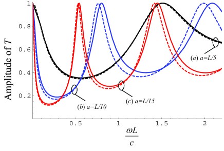
To begin with, we study the frequency response of the metamaterial slab for plane wave incidence. In Fig. 2 the transmission coefficient is plotted as function of frequency for a fixed thickness and for different values of the lattice constant : , and (solid lines). The wires are assumed to be PEC, and the angle of incidence is . In all the examples, the amplitude of the transmission coefficient is approximately unity in the static limit . This is consistent with the fact that for low frequencies the length of the wires () is electrically short, and thus at the wires may interact weakly with the incoming wave. However, quite remarkably and despite the fact that the wires are very short, for frequencies slightly above the transmission coefficient may have several dips and the incoming wave may be strongly reflected by the structured substrate. For example, when the lattice constant is (curve (c)), has a dip for , which corresponds to metallic wires with length . This length is one order of magnitude lower than the traditional resonance length for a PEC wire. The unusual electrical response of the crossed wire mesh (formed by very short wires) is caused by the strong interaction between the fields guided by each set of wires and the other set of perpendicular wires, which results in an anomalously high positive effective index of refraction Silveirinha and Fernandes (2008).
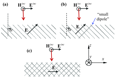
This mechanism can be understood by analyzing Fig. 3, where the crossed wire mesh [panel (c)] is constructed step by step starting from an array of parallel wires [panel (a)], to which the perpendicular wires are sequentially added [panel (b)]. For simplicity, it is supposed that in the scenarios depicted in Fig. 3 the incoming wave illuminates the slab along the normal direction, and that the host material is air. Consider first the configuration reported in panel (a), which portrays the case where the array of parallel wires is tilted by an angle (not necessarily ) with respect to the interface. It is known from previous studies Silveirinha et al. (2008) that when the wires are densely packed () the dominant electromagnetic mode excited in such structure is the so-called “transmission line” mode Belov et al. (2003). This mode is a transverse electromagnetic (TEM) wave, and hence the average electric field inside artificial material is orthogonal to the wires, as represented in panel (a). The fields inside the material propagate along the direction of the wires with the velocity of light, and the propagation constant along the direction is (assuming that the incoming wave propagates along the normal direction) Silveirinha et al. (2008). Hence, , at least as long as is not too large, which is the situation of interest here. How can we increase , so that the effective index of refraction seen by the wave in the material may be very large? A possible solution is to add suitable inclusions to the metamaterial so that the path of the transmission line wave is partially obstructed by these inclusions resulting in a greater phase delay. Since from panel (a) it is known that the electric field is orthogonal to the wires, the obvious solution is to add a “small wire dipole” that will partially block the electric field associated with the original transmission line mode [solution represented in panel (b)]. Naturally, in order to obtain a significant phase delay many of such “small wire dipoles” are necessary, and hence we arrive at the completely symmetric crossed wire mesh configuration shown in panel (c). It is important to note that the array of “added wires” does also support transmission line modes when it stands alone in free-space. However, quite interestingly, such TEM wave is delayed by the original set of wires [represented in panel (a)], precisely in the same manner as the “added wires” delay the TEM wave supported by the original set of wires. In fact, when the crossed wire mesh becomes completely symmetric and the roles of two sets of wires can be interchanged. It is also clear that for symmetry reasons the average electric field inside the artificial material becomes parallel to the incident field when the second array of wires is added to the structure. The described interaction mechanism is the physical reason for the very large index of refraction of the crossed wire mesh. It is important to mention that the crossed wire mesh supports a propagating mode at very low frequencies (with the electric field polarized along the -direction) only when the two sets of wires are physically disconnected, as assumed here. Indeed, when the two sets of wires are connected it is possible to find a continuous (“zigzag”) path along the metallic wires that runs from to . This continuous metallic channel would effectively block an incoming wave (with the electric field along the -direction), and confer the material plasmonic-like properties. Quite differently, when the two sets of wires are nonconnected, any continuous path running along the wires has finite length, and consequently propagation becomes possible at low frequencies.
As shown in Silveirinha and Fernandes (2008), for a fixed frequency the effective index of refraction of the propagating mode, , ( is given by the solution of Eq. (3) associated with the “+” sign), can be made arbitrarily large by increasing the density of wires, i.e. by making . Such phenomenon can be readily understood in light of the interaction mechanism explained in the previous paragraph. In fact, as the density of wires increases the wave guided by each set of wires suffers a greater phase delay, resulting in a larger effective index of refraction. The results of Fig. 2 are consistent with this property, since as is made smaller the electric response of the structure becomes stronger for lower frequencies. In fact, notwithstanding the extremely small electrical length of the wires, theoretically it is possible to move the first dip of transmission coefficient to an arbitrarily small frequency by reducing and keeping the metal volume fraction constant (). This property is only limited by the effect of metallic loss, which may be relevant when the radius of the wires becomes smaller than the skin depth of the metal Silveirinha and Fernandes (2008). The reported results are fully confirmed by full wave simulations obtained using the electromagnetic simulator CST Microwave StudioTM CST (http://www.cst.com) (dashed lines in Fig. 2), which show a remarkable agreement with our analytical model.
III Enhancement of evanescent waves
The high index of refraction of the material may enable the propagation of ultra-subwavelength guided modes Silveirinha and Fernandes (2008); Silveirinha et al. (accepted for publication in Appl. Phys. Lett.). This suggests that a thin material slab may be used to enhance evanescent waves, and in this way obtain a superlensing effect. In order to investigate this possibility in Fig. 4 we plot the amplitude of as a function of the transverse wavenumber of the impinging wave, , for different frequencies of operation . The wires are assumed to be PEC and the slab has a fixed thickness . The solid curves correspond to the analytical model [Eq. (5)], whereas the dashed lines were calculated using CST Microwave StudioTM CST (http://www.cst.com).
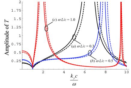
It is seen that the transfer function may have several resonances, which correspond to the excitation of guided modes. For very low frequencies (not shown in Fig. 4), the pole of occurs for some transverse wavenumber such that is slightly above unity, consistently with the fact that near the static limit most of the energy of the guided mode is concentrated outside the material slab. The remarkable property is that due to extreme effective parameters of the composite material the guided mode may become extremely attached to the metamaterial slab even for extremely long wavelengths. For example, in curve (a) the pole occurs at , notwithstanding the extremely small thickness of the slab thickness, , and the very small length of the wire inclusions (). As illustrated in curve (b), as the frequency increases the value of associated with the guided mode increases even more, which indicates that the mode becomes even more attached to the structured substrate. For even larger frequencies [curve (c)], an additional guided mode is supported, and as a consequence two distinct resonances are seen in Fig. 4.
From the results of Fig. 4, it may be inferred that the optimal frequency to obtain subwavelength imaging is such that [curve (a)]. In fact, for such frequency the evanescent waves may be significantly amplified over a relatively wide range of values of centered at the pole of . It should be noticed that at the same frequency the amplitude of the transmission coefficient for propagating waves () is relatively small. This further helps to enhance the subwavelength spatial spectrum (which is attenuated in the free-space regions) in comparison to propagating plane waves (which propagate with no attenuation in free-space). Indeed, from curve (b) of Fig. 2 it may be verified that corresponds to a minimum of for incidence along the broadside direction. The results of our simulations indicate that the described property is also observed for other lens parameters, and that the value of that enables the best imaging is such that has a minimum for normal incidence.
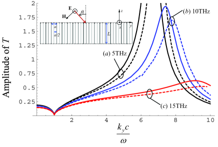
The enhancement of evanescent waves has a good tolerance to the effect of metallic loss. In order to demonstrate this, we plot in Fig. 5 the transfer function of a system with the same parameters as the one associated with curve (a) of Fig. 4, except that now the effect of metallic loss if fully considered. The wires are assumed to be made of silver, which is modeled using a Drude dispersion relation, consistent with the experimental results tabulated in Ordal et al. (1985). It can be noticed that at 5THz [curve (a) in Fig. 5] the transfer function of the system formed by silver wires is rather similar to that of a system formed by PEC wires [curve (a) in Fig. 4]. Indeed, at 5THz the skin depth of silver is approximately while the radius of the wires is , and since is relatively close to unity the effect of metallic loss is still quite moderate. As mentioned before, the effect of metallic loss is negligible provided Silveirinha and Fernandes (2008). At 10THz [curve (b)] the response of the system becomes distinctively different from the PEC case, consistent with the fact that the ratio increases [ and ]. At 15THz [curve (c)] the effect of loss is strong [ and ] and there is no amplification of evanescent modes. Thus, we may conclude that the proposed superlens may be feasible at least up to 10THz. For frequencies below 5THz the conducting properties of silver improve and the transfer function of a scaled superlens formed by silver wires becomes nearly coincident with that of a superlens formed by PEC wires.
IV Imaging a line source
To further characterize the imaging properties of the considered structure, in the following we study the canonical problem where an electric line source (infinitely extended along the -direction) is placed at a distance above the crossed wires slab (see the inset of Fig. 6). The electric field radiated by the line source is of the form , where is some constant that depends on the line current, is the radial distance to the source, and is the Hankel function of second kind and order zero. Assuming that the metamaterial slab is unbounded along the directions and , it is straightforward to find that the electric field at a distance below the slab is given by the Sommerfeld-type integral:
| (6) |
where , and is the transfer function of the slab given by Eq. (5).
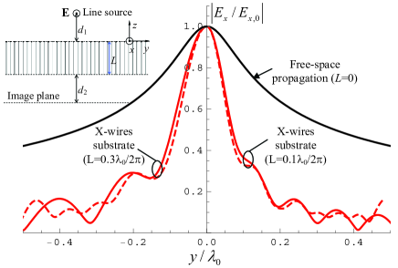
Using the above formula we have calculated the electric field profile at the image plane for an artificial material slab with the same parameters as curve (a) in Fig. 4 ( and ). It was assumed that , and that the source is in the plane . The normalized electric field at the image plane is depicted in the left-hand side panel of Fig. 6 (solid red line) as a function of . The half power beam width (HPBW) is equal to HPBW=, which is 4 times smaller than the traditional diffraction limited value. The normalized electric field at the image plane when the superlens is absent and the distance between the source and the image plane is , is also shown in Fig. 6 (solid black line). Notice that when the lens is present the total distance between the source and the image plane is , while when the lens is absent the distance is reduced to . Notwithstanding the greater proximity between the source and the image plane, in the latter case the half power beam width increases to HPBW=. For the propagating distance in free-space, the half power beam width is HPBW=. These properties demonstrate that the considered artificial material slab behaves as a superlens with effective “negative length”. In fact, the insertion of the superlens in between the source and the image plane results in a significantly narrower beam than when the lens is absent, as if the total distance between the source and the image plane had been decreased. This effect stems from the resonant excitation of guided modes, which effectively compensate for the attenuation of evanescent waves in the free-space regions, and in this way enable imaging with subwavelength resolution. The resolution of the proposed superlens is , despite the source and observation planes being located at a significant distance from the lens interfaces.
A slab with a larger density of wires may provide an even better resolution. This is illustrated in the right-hand side panel of Fig. 6 (solid red line), for the case in which , and . The distances between the source and image planes are kept the same as in the previous example, so that . The increased density of wires results in a larger effective index of refraction of the slab, and this enhances the response of the system () for a wider range of evanescent waves. As a consequence, the half power beam width of the superlens is improved to HPBW=. The value of HPBW may obviously be made much smaller if is taken closer to unity, as in a standard silver lens Pendry (2000); Fang et al. (2005).
The described results were obtained using the analytical model [Eq. (6)], and assume that the structured material slab is infinitely extended along the and directions. In order to confirm the homogenization results, a finite width superlens was modeled using a dedicated periodic Method of Moments (MoM) code. The Method of Moments fully takes into account all the fine details of the microstructure of the crossed wire mesh. In the MoM simulation the artificial material slab was assumed periodic along the -direction, and finite along the -direction. The width of superlens was taken equal to (901 rows of wires along the direction spaced by ) in the case where the thickness of the lens is , and (2401 rows of wires along the direction) in the case where . The calculated electric field profiles at the image plane are depicted in Fig. 6 (dashed red line) showing a remarkable agreement with the homogenization results, despite that the homogenization results refer to an unbounded substrate, whereas the MoM simulations refer to finite width substrate. The results of our simulations (not shown here for brevity) suggest that this property may also hold for other widths of the substrate such that , where is an integer. On the other hand, we found out that when is slightly larger than an odd multiple of the reflection of surface waves at the edges of the slab may significantly corrupt the quality of the imaging.
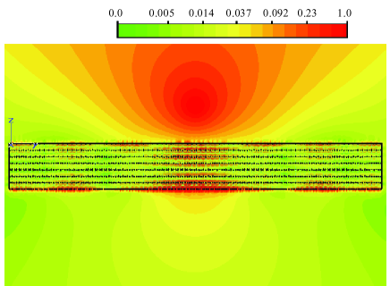
We have also studied the performance of the proposed superlens using the commercial electromagnetic simulator CST Microwave StudioTM CST (http://www.cst.com). The geometry of the structure was taken the same as that of case (i) in Fig. 6, except that (due to limited computational resources) the width of slab along was reduced to (162 rows of wires). The amplitude of the electric field is represented in Fig. 7, showing that despite the relatively small aperture of the lens the beam width (measured along the along the -direction) of the transmitted wave is very subwavelength, consistent with the MoM simulations reported in Fig. 6. The imaging dynamics can be visualized in the electric field animation reported in EPA (movie stored in EPAPS). It is interesting to note that despite the propagating spatial harmonics not being matched to the lens, the effects of reflection are hardly perceptible in the field animation. This happens because the distance between the source and the lens is electrically small (), and interference effects are difficult to visualize within such short distance.
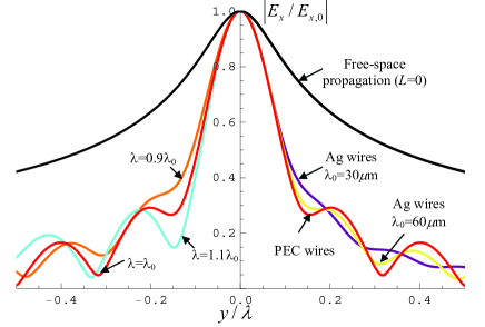
The described superlensing effect is relatively insensitive with respect to variations of the frequency of operation. This is shown in the left-hand side panel of Fig. 8, where it is seen that for the same design as in case (i) of Fig. 6 (for an unbounded substrate) the electric field profile remains nearly invariant when the wavelength of operation is taken either or . This is a consequence of the non-resonant nature of the effective parameters of the structured material Silveirinha and Fernandes (2008). The variation of the peak level of with respect to the case is less than 8 percent in both cases. The imaging quality is significantly deteriorated only when the frequency of operation is such that corresponds to a maximum of for plane wave incidence along the broadside direction.
Likewise, the imaging properties have a good tolerance to the effect of metallic loss. In the right-hand side panel of Fig. 8 the profile of the imaged electric field is shown for a scaled superlens made of silver wires at (5THz) and (10THz). Consistent with the results of Fig. 5, it is seen that apart from a reduced ripple in the electric field tail (due to the greater attenuation of the guided modes supported by the metamaterial slab), the half power beamwidth remains very similar to the PEC case. The relative amplitude of the transmitted wave with respect to the PEC case is 0.96 at 5THz and 0.84 at 10THz. This suggests that the proposed structure may have exciting applications at terahertz frequencies.
V Conclusion
It was demonstrated that a crossed wire mesh slab may enable a imaging with subwavelength resolution. It was discussed that the extreme effective parameters of the crossed wire mesh permit the propagation of ultra-subwavelength guided modes. These guided modes may be excited by the near-field evanescent spectrum of a given source, and this mechanism, somehow analogous to that characteristic of a silver superlens Pendry (2000); Fang et al. (2005), may permit the enhancement of evanescent waves and of the near field details. We presented an analytical model that describes very accurately the electromagnetic response of the proposed imaging device. For a specific design, and despite the distance between the source and observation planes and the lens interfaces being comparable to the lens thickness, the resolution was demonstrated. The effect of metallic loss was analyzed, and it was shown that it may be relatively mild provided the radius of the metallic rods is kept smaller than the metal skin-depth. It is envisioned that the proposed system may find interesting applications at the microwave and terahertz regimes.
VI Acknowledgment
This work is supported in part by Fundação para a Ciência e a Tecnologia, grant number No. POSC/EEACPS/61887/2004.
References
- Pendry (2000) J. Pendry, Phys. Rev. Lett. 85, 3966 (2000).
- Taubner et al. (2006) T. Taubner, D. Korobkin, Y. Urzhumov, G. Shvets, and R. Hillenbrand, Science 313, 1595 (2006).
- Fang et al. (2005) N. Fang, H. Lee, C. Sun, and X. Zhang, Science 308, 534 (2005).
- Freire and Marques (2005) M. J. Freire and R. Marques, Appl. Phys. Lett. 86, 182505 (2005).
- Belov et al. (2006) P. A. Belov, Y. Hao, and S. Sudhakaran, Phys. Rev. B. 73, 033108 (2006).
- Salandrino and Engheta (2006) A. Salandrino and N. Engheta, Phys. Rev. B 74, 075103 (2006).
- Liu et al. (2007) Z. Liu, H. Lee, Y. Xiong, C. Sun, and X. Zhang, Science 315, 1686 (2007).
- Smolyaninov et al. (2007) I. I. Smolyaninov, Y.-J. Hung, and C. C. Davis, Science 315, 1699 (2007).
- Merlin (2007) R. Merlin, Science 317, 927 (2007).
- Silveirinha and Fernandes (2008) M. G. Silveirinha and C. A. Fernandes, Phys. Rev. B 78, 033108 (2008).
- Silveirinha et al. (accepted for publication in Appl. Phys. Lett.) M. G. Silveirinha, C. A. Fernandes, J. R. Costa, and C. R. Medeiros (accepted for publication in Appl. Phys. Lett.).
- Belov et al. (2008) P. A. Belov, Y. Zhao, S. Tse, P. Ikonen, M. G. Silveirinha, C. R. Simovski, S. Tretyakov, Y. Hao, and C. Parini, Phys. Rev. B 77, 193108 (2008).
- Silveirinha and Fernandes (2005a) M. G. Silveirinha and C. A. Fernandes, IEEE Trans. on Antennas and Propagat. 53, 59 (2005a).
- Silveirinha and Fernandes (2005b) M. G. Silveirinha and C. A. Fernandes, IEEE Trans. on Microwave Theory and Tech. 53, 1418 (2005b).
- Simovski and Belov (2004) C. R. Simovski and P. A. Belov, Phys. Rev. E 70, 046616 (2004).
- Silveirinha et al. (2008) M. G. Silveirinha, C. A. Fernandes, and J. R. Costa, New J. Phys. 10, 053011 (2008).
- CST (http://www.cst.com) CST Microwave Studio 2006, CST GmbH (http://www.cst.com).
- Belov et al. (2003) P. Belov, R. Marques, S. Maslovski, I. Nefedov, M. Silverinha, C. Simovski, and S. Tretyakov, Phys. Rev. B 67, 113103 (2003).
- Ordal et al. (1985) M. A. Ordal, R. J. Bell, R. W. Alexander-Jr, L. L. Long, and M. R. Querry, Applied Optics 24, 4493 (1985).
- EPA (movie stored in EPAPS) Time-domain animation of the electric field component associated with the configuration of Fig. 7 (movie stored in EPAPS).