Electron tunneling into a quantum wire in the Fabry-Pérot regime
Abstract
We study a gated quantum wire contacted to source and drain electrodes in the Fabry-Pérot regime. The wire is also coupled to a third terminal (tip), and we allow for an asymmetry of the tip tunneling amplitudes of right and left moving electrons. We analyze configurations where the tip acts as an electron injector or as a voltage-probe, and show that the transport properties of this three-terminal set-up exhibit very rich physical behavior. For a non-interacting wire we find that a tip in the voltage-probe configuration affects the source-drain transport in different ways, namely by suppressing the conductance, by modulating the Fabry-Pérot oscillations, and by reducing their visibility. The combined effect of electron electron interaction and finite length of the wire, accounted for by the inhomogeneous Luttinger liquid model, leads to significantly modified predictions as compared to models based on infinite wires. We show that when the tip injects electrons asymmetrically the charge fractionalization induced by interaction cannot be inferred from the asymmetry of the currents flowing in source and drain. Nevertheless interaction effects are visible as oscillations in the non-linear tip-source and tip-drain conductances. Important differences with respect to a two-terminal set-up emerge, suggesting new strategies for the experimental investigation of Luttinger liquid behavior.
pacs:
73.23.-b, 71.10.Pm, 73.23.Ad, 73.40.GkI Introduction
Electron scanning of a conductor with a probe terminal is a customary technique to investigate its local properties. The local density of states can be gained from the dependence of the tunneling current on the applied bias. Nowadays, atomically resolved images are obtained both with scanning tunnel microscopes (STM) and atomic force microscopes (AFM).NW-1 So far, most of the efforts of the scientific community have focused on improving the resolution power of the probe terminal. For instance, the recent realization of stable and sharp superconducting STM tips exploits the singularity in the quasiparticle density of states to this purpose.NW-2 A probe terminal, however, may also be used as a “handle”, i.e. as an active component to tune the transport properties of the conductor. Recent works in this direction have shown that the sign of the supercurrent can be changed when a third terminal injects electrons into a Josephson junction under appropriate conditions,NW-3 that the conductance of a quantum dot can be tuned by moving an AFM tip over the sample,NW-4 or that a single-electron transistor can be used to cool down a nanomechanical resonator, or to drive it into a squeezed state.Schwab
The promising applications of scanning probes in the study of transport properties of nanodevices require a theoretical analysis of electron transport in a three-terminal set-up, a subject which has been explored only partly so far. In particular, most of the available investigations are restricted to the case of non-interacting conductors,NW-5 ; voltage-probe-refs whereas relatively little attention has been devoted to those nanodevices in which electronic correlations play a dominant role. This is the case for one-dimensional (1D) conductors, such as semiconductor heterostructure quantum wiresNW-6 and single-walled carbon nanotubes.NW-7 ; liang:2001 There, electron-electron interaction dramatically affects the dynamics of charge injection. The response of the system to the scanning probe is quite different from that of ordinary three dimensional metals, since in 1D electronic correlations lead to a breakdown of the Fermi liquid picture. Semiconductor quantum wires and carbon nanotubes rather exhibit Luttinger liquid (LL) behavior.NW-8 ; yacoby ; nanotube-LL ; yamamoto:2007 While for this type of systems two-terminal electron transport has been widely analyzed in the last 15 years,NW-6 ; NW-7 ; NW-8 ; yacoby ; nanotube-LL ; liang:2001 ; yamamoto:2007 the electric current and noise in a three-terminal set-up, including source and drain electrodes and a tip, have remained mostly unexplored.
There are, however, a few notable works in this direction. The case where a bias is applied between a tip and a semi-infinite LL was investigated by Eggert,NW-9a and by Ussishkin and Glazman.NW-9b Martin and co-workersmartin:2003 ; martin:2005 have recently analyzed the electric noise of the current injected from a tip into a nanotube adiabatically contacted at each end to grounded metallic leads.
In this paper we extend these investigations to a quite general three-terminal set-up. We shall thus explore the non-equilibrium current in all three terminals in presence of a transport voltage between the source and drain electrodes, an applied tip voltage, and also a tunable gate voltage. This enables us to address various physical phenomena that are of relevance for recent experiments. Among other effects, we discuss the influence of the tip on the transport along the interacting wire, even when no net current is injected from the tip into the wire. In particular, we focus on the Fabry-Pérot transport regime of the wire, which could be recently observed in carbon nanotubesliang:2001 ; yamamoto:2007 ; hakonen:2007 ; kontos:2007 , and analyze how Fabry-Pérot oscillations are modified by both the presence of the tip and the electron-electron interaction. To this purpose, the finite length of the wire, the contact resistances at the interfaces between the wire and the side electrodes, as well as an arbitrary position of the tip along the 1D wire are taken into account in our model. Furthermore, inspired by recent experiments on semiconductor quantum wiresyacoby ; yacoby:2 , we allow for an asymmetry in electron tunneling from the tip, and investigate how the presence of side electrodes affects the fractionalization of charges injected by the tip into an interacting wire. Finally, regarding the experimental observation of interaction effects, we discuss the advantages of a three-terminal set-up over a two-terminal one.
The paper is organized as follows. In Sec. II we describe the model that we adopt for the set-up. In Sec. III we provide results about the electric current in the case of a non-interacting wire, while Sec. IV is devoted to the effects of electron-electron interaction. Finally, we shall discuss the results in Sec. V and present our conclusions. Some more technical details are given in the appendices.
II The model
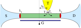
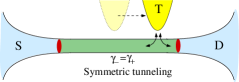
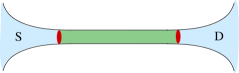
We consider a single channel spinless quantum wire connected, as sketched in Fig. 1, to two metallic electrodes, source (S) and drain (D), as well as to a third sharp electrode, henceforth denoted as tip (T). The wire has a finite length and for the coordinate along it we choose the origin in the middle of the wire so that the interfaces to the S and D electrodes are located at and , respectively. Electron backscattering at the side contacts due to non-adiabatic coupling is modeled by two delta-like scatterers. The tip is described as a semi-infinite non-interacting Fermi liquid, and denotes the coordinate axis along the tip orthogonal to the wire, the origin corresponding to the injection point on the tip. The latter is located at position with respect to the middle of the wire, and electron injection is modeled by a tunnel Hamiltonian. We also envisage the presence of a metallic gate (G), biased at a voltage . Screening by this gate yields an effectively short-ranged electron-electron interaction potential within the wire, for which the LL model applies.safi-schulz ; maslov-stone ; nota-short-range The total Hamiltonian of the system reads
| (1) |
where the first term describes the wire and its coupling to the S and D electrodes as well as to the gate. The second term accounts for the tip, and the last one describes wire-tip tunneling.
As far as the wire is concerned, we shall address here the low-energy regime, where the wire electron band can be linearized around the Fermi level. Then the wire electron operator can be decomposed into right- and left-moving components and
| (2) |
where denotes the equilibrium Fermi momentum of the wire. By definition, this is the Fermi momentum in case that the electrochemical potentials of all electrodes, source, drain, tip and gate, are identical. This corresponds to vanishing applied voltages. Explicitly the Hamiltonian of the wire reads
| (3) |
In Eq. (3) the first term
| (4) | |||||
describes the band energy linearized around the wire Fermi points and characterized by a Fermi velocity . The symbol stands for normal ordering with respect to the equilibrium ground state. The second term models scatterers at the interfaces NW-15 ; recher-PRB with the S and D electrodes
| (5) |
where the dimensionless parameters denote the impurity strengths at the contacts , and the term = :: is the electron density fluctuation with respect to the equilibrium value. The third term in Eq. (3),
| (6) |
with
| (7) |
accounts for the bias and of the source and drain electrodes, as well as for the gate voltage . The applied transport voltage is then . Finally, the last term
| (8) |
describes the screened Coulomb interaction in the wire,safi-schulz ; maslov-stone where = :: is the density fluctuation of -moving electrons. As it is customary in LL theory, in the sequel, we characterize the interaction strength by the dimensionless coupling constant
| (9) |
The Hamiltonian of the tip, the second term in Eq. (1), reads
| (10) |
Here
| (11) |
describes the (linearized) band energy with respect to the equilibrium Fermi points of the tip, and denotes the Fermi velocity. Notice that the integral runs also over the positive -axis, since right and left moving electron operators along the physical tip axis have been unfolded into one chiral (right-moving) operator defined on the whole -axis. The second term in Eq. (10) describes the bias applied to the tip which affects the incoming electrons according to
| (12) |
Finally, the third term in Eq. (1) accounts for the wire-tip electron tunneling and reads
| (13) |
where is the dimensionless tunneling amplitude for -moving electrons, and [] is the coordinate of the injection point along the wire [tip]. Here, we have allowed for a right/left asymmetry of electron tunneling between the tip and the wire, which can arise from the presence of a magnetic fieldyacoby ; yacoby:2 ; yacoby-lehur . Note that for the Hamiltonian is not invariant under time-reversal symmetry.
In the following sections the electron current will be evaluated in the three terminals of the described set-up. Explicitly we shall compute
where , with , is a measurement point located in the S or D leads. As far as the tip is concerned, due to the unfolding procedure described above, the electron current flowing in the tip at a point acquires the form
| (15) |
In Eqs. (LABEL:I-W) and (15) the averages are computed with
respect to the stationary state in presence of the applied dc
voltages , , and .
Under these conditions, the current in each electrode is actually independent of the measurement point. We thus denote by and the currents flowing in the source and drain electrodes. The current is positive when flowing into the wire, while is positive when flowing out of the wire. The current flowing in the tip is positive when flowing in the direction of the tip-wire tunnel contact. Current conservation then implies , so that all currents can be expressed in terms of two independent quantities. One can write
| (16) | |||||
| (17) |
where describes the current flowing in the wire under the condition that no net current flows through the tip (voltage probe configuration). Importantly, should not be identified with the two-terminal current flowing in the absence of the tip. Indeed, while implies that , the opposite does not hold, so that needs to be evaluated by accounting for the whole three-terminal set-up.
III The non-interacting case
In this section we first discuss results for the case that the electron interaction (8) is neglected. Then the Hamiltonian (1) of the whole system is quadratic in the fields and , and transport properties can be determined within the Landauer-Büttiker formalism. In the three-terminal set-up that we are considering, the scattering matrix is a matrix which depends on the energy measured with respect to the equilibrium wire-lead Fermi level. The currents and defined through Eq. (16) and (17) read
and
| (19) | |||||
In the -matrix elements appearing in Eqs. (III) and (19) the source, drain and tip electrodes are identified as 1, 2, and 3 respectively, whereas their Fermi functions are denoted as , and . Note that the -matrix is in general not symmetric, because time-reversal symmetry is broken for . The -matrix can straightforwardly be evaluated with standard techniques by combining the transfer matrices () of the two side contacts
| (20) |
with the one, , at the tip injection point
| (21) |
Here, we have introduced the ballistic frequency
| (22) |
associated with the length of the wire, and the following dimensionless quantities
| (23a) | ||||
| (23b) | ||||
| (23c) | ||||
| (23d) | ||||
The scattering matrix is obtained as a combination of the elements of the transmission matrix in the form
where are the matrix elements of .
III.1 Fabry-Pérot oscillations in a two-terminal set-up
Before discussing the influence of the STM tip, we shortly describe the transport properties in the absence of the tip, i.e. for . In this case we have a two-terminal set-up with and . The solid line in Fig. 2 shows the two-terminal conductance at zero temperature plotted in units of as a function of the (dimensionless) source-drain bias
| (25) |
for identical contact impurity strengths . For the conductance shows the typical Fabry-Pérot oscillations with maximum values close to one. For carbon nanotubes the Fabry-Pérot regime of highly transparent contacts could be reached experimentally only recently due to progress achieved in device contacting.liang:2001 ; yamamoto:2007 ; hakonen:2007 ; kontos:2007 In the sequel, we will focus on this regime.
The electron current can be written as
| (26) |
where represents the current of a perfectly contacted wire, and characterizes the (negative) correction due to the contact resistances. The exact expression for , which can be gained from the -matrix, is not easily tractable for arbitrary impurity strengths and temperature. In the Fabry-Pérot regime at zero temperature, however, a simpler expression is obtained by expanding in terms of the impurity strengths. To third order in the ’s one obtains
| (27) |
where and are dimensionless quantities describing the incoherent and coherent contributions, respectively, to the reduction of the current by the contact impurities. The term
| (28) |
is linear in the applied bias voltage, and the coefficient of proportionality is the “classical” series resistance of two impurities. In contrast, the term stems from quantum interference between scattering processes. This interference leads to the Fabry-Pérot oscillations of . Explicitly,
| (29) |
where
| (30) |
and
| (31) |
where we have introduced
| (32) |
From Eqs. (30)-(31) one can see that Fabry-Pérot oscillations arise both as a function of the source-drain bias and as a function of the gate voltage . Note that for a non-interacting system the period in the former case is twice as large as the period in the latter case.
We also emphasize that originates from impurity forward-scattering processes (more precisely from second order in backward scattering and first order in forward scattering). Forward scattering processes are typically neglected in single impurity problems, where they can be gauged away. However, when two or more impurities are present they affect the coherent part of transport. Although this contribution is in general smaller than , it becomes the dominant term for the Fabry-Pérot oscillations when vanishes, which is the case for
| (33) |
Thus, the third order term is crucial for certain values of the biasing voltage.
We conclude the discussion of the two-terminal case by emphasizing that for a non-interacting wire in the Fabry-Pérot regime the current depends not only on the difference , but in general on and separately. This is simply due to the fact that Fabry-Pérot interference effects lead to an energy-dependent transmission coefficient and, hence, to non-linearity in the applied bias. Notice that Eqs. (28), (30) and (31) fulfill the gauge-invariance condition emphasized by Büttiker,buttiker:1993 since they are invariant under an overall shift of the potentials ().
III.2 Effect of the tip on Fabry-Pérot oscillations
In this section we shall address, within the non-interacting electron approximation, the effect of the STM tip on the Fabry-Pérot oscillations. When , the currents and are non-vanishing for arbitrary values of the applied voltages , and . We analyze the effects of the tip as a function of the total tunneling strength , defined through
| (34) |
the tunneling asymmetry coefficient
| (35) |
and the position of the tip.
We start by considering the situation where the tip behaves as an electron injector: a bias is applied between the tip and the source and drain electrodes, which, for simplicity, are assumed to be at the same electrochemical potential. A quite standard calculation applies to the case of fully symmetric tunneling (), allowing, e.g., to relate the local density of states in the wire to the non-linear conductance as a function of the tip-wire bias. Here, we shall instead focus on the case of fully asymmetric tunneling (), which has become of particular interest due to recent experiments where only right-moving and/or only left-moving electrons could be selectively tunneled into a semiconductor quantum wire due to the presence of a magnetic field normal to the plane of the wire and the tip.yacoby:2 We find that novel physical aspects emerge from a tunneling asymmetry. In the first instance, a direct inspection of the scattering matrix (III) shows that its elements are independent of , implying that, differently from the case of symmetric tunneling , the lead currents and do not depend on the position of the tip. Furthermore, asymmetric tunneling can be used to extract the transmission coefficient of each contact. Indeed evaluating the asymmetry
| (36) |
between and in the two cases of totally asymmetric injection only to the right () and only to the left (), one obtains
| (37) |
and
| (38) |
where . From these coefficients it is straightforward to extract the strengths of the contact impurities
as well as the transmission coefficients
| (40) |
related to each of the two contacts.
Notice that, while and depend on the temperature ,
Eqs. (37) and (38) are independent of
within the approximation of a linearized band.
Interestingly, these equations also enable one to identify the relation between the current asymmetry coefficients and the two-terminal conductance . In Ref. yacoby-lehur, , the equality is
claimed to hold for a set-up with symmetric contacts to the leads,
even in the presence of interactions. However,
Eqs. (37) and (38) show that for a
quantum wire in the Fabry-Pérot regime, even in the absence of
interactions and with perfectly symmetric contacts , one has
| (41) |
since is a constant,
whereas depends on temperature, source-drain bias and gate voltage.
The equality sign in Eq. (41) holds only
under the specific circumstances of
perfectly transmitting contacts (), or of
a perfectly symmetric set-up () at sufficiently high temperatures , where Fabry-Pérot oscillations of wash out.
The second situation that we want to investigate is
when the tip voltage is set to an appropriate value
so that no net current flows through the tip. This corresponds to a situation where the tip behaves as a voltage probeNOTA-voltageprobe . Notice that, even under the condition ,
electrons can tunnel from the tip to the wire and vice
versa, and therefore the tip does affect the electron transport
between source and drain.
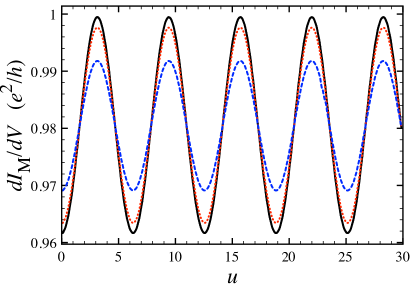
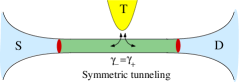
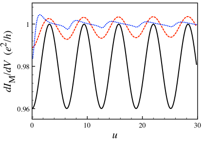
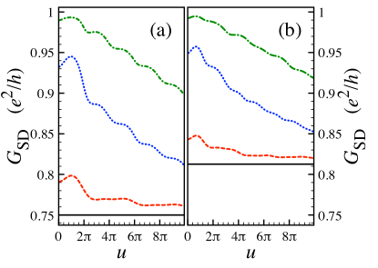
We start by describing the case of symmetric tunneling () with the tip located in the middle of the wire (). The differential conductance , evaluated under the condition , is depicted in Fig. 2 as a function of the source-drain bias (25), for different values of , ranging from weak to strong tunneling. The tip has three main effects on the Fabry-Pérot oscillations: i) an overall suppression of the conductance, ii) a modulation of the maxima and minima, and iii) a reduction of the visibility of the oscillations.
The origin of the first effect can be illustrated already in the case of a clean wire (), where it is easy to show that the condition is fulfilled for a tip voltage , and that
| (42) |
Notice that a reduction of the conductance already shows up to order in the tunneling strength. The reason for this suppression of the current is that a fraction of the electron flow originating from the source is diverted into the tip due to the tip-wire coupling. While the condition ensures that the same electron current is re-injected into the wire, for symmetric tunneling the tip injects with equal probabilities right and left moving electrons. Hence half of the injected current flows back to the source electrode, causing the reduction of the two-terminal conductance. As we shall see below, the situation is different in the case of asymmetric tunneling.
The second feature that can be observed in Fig. 2 is an alternating depth of the Fabry-Pérot minima. This modulation originates from the interference between different paths that are possible for an electron ejected from the tip. For instance, the path of an electron ejected as right mover towards the drain can interfere with the path starting as left mover towards the source followed by an elastic backscattering at the source contact. The difference in length between these paths corresponds to a new frequency in the oscillations, which causes the modulation of the peaks. In the case of Fig. 2, where the tip is located in the middle, this additional frequency equals twice the Fabry-Pérot frequency, so that the tip affects every second minimum in the same way. As we shall see below, in general, the modulation pattern depends both on the asymmetry coefficient and on the position of the tip. The modulation effect arises to order when we treat the impurity strength and tunneling amplitudes as perturbation parameters.
The third effect of the tip consists in a reduction of the visibility of the the Fabry-Pérot oscillations: in the presence of the tip the relative separation between maxima and minima decreases. This reduction stems from the decoherence introduced by the tip, since the probability of constructive interference between paths with two backscattering processes at the contacts decreases when electrons can be incoherently absorbed and re-ejected by the tip. Notice that the reduction of visibility is of order , and it is therefore negligible with respect to the modulation effect in the Fabry-Pérot regime.
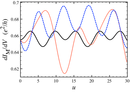
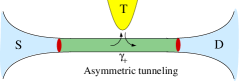
Let us now discuss the role of asymmetric tunneling in the voltage probe configuration. When , the effect of conductance suppression is less pronounced then for symmetric tunneling. This can be seen already in the case of a clean wire (), where
| (43) |
and the value of the tip voltage ensuring is given by
| (44) |
As one can see from the last factor in Eq. (43), the
suppression of the current is completely absent for
fully asymmetric tunneling . Importantly, this
features persists also in the presence of realistic contacts
(), as shown in Figure 3, where
the differential conductance is plotted as a
function of the source-drain voltage for several values of the
tunneling strength . Increasing the tunneling strength
simply decreases the amplitude of the Fabry-Pérot oscillations
but does not change the average value of the conductance. Two
more noteworthy features can be observed: in the fully asymmetric
case also the modulation of the peaks is absent, and the
non-linear conductance is independent of the tip position. The
reason lies in the specific tunneling conditions. For example, a
right moving electron ejected by the tip cannot be re-adsorbed
after scattering as a left moving one, and this rules out
interference effects between electrons traveling through the tip
and electrons that have undergone an odd number of backscattering
events at the contacts. Such processes would give rise to effects
related to the tip position, while interference phenomena with
electrons that have undergone an even number of backscattering
events, which continue to be present also for , are
independent of the tip position. Moreover, in the completely
asymmetric case, electrons passing through the tip continue to
move in the same direction, and this is the reason why, also for
strong tunneling, the average value of the
differential conductance is independent of .
Finally, we analyze the dependence of the differential conductance on the tip position. For simplicity we limit this discussion to the case of symmetric tunneling illustrated in Fig. 4. Apart from the conductance suppression discussed above, one sees that the modulation effect exhibits a strong dependence on the tip position. In particular, when the tip is close to a contact impurity, we observe Fabry-Pérot-like oscillations over-imposed by an oscillation with large period due to coherent motion of carriers between the tip and the contact impurity remote from the tip.
IV The interacting case
In this section we discuss the three terminal set-up in presence of electron-electron interaction. For arbitrary values of the interaction strength, contact resistances, and tunneling amplitudes an analytical treatment is not possible, therefore we focus here on the Fabry-Pérot regime. In this regime, characterized by highly transparent contacts to the electrodes, the role of interactions has so far only been analyzed for a two terminal set-up.NW-15 ; recher-PRB Since the impurity strengths are small, they can be treated perturbatively. The electron-electron interaction (8) will be accounted for exactly using bosonization. The evaluation of the currents in the three terminals will be based on the out-of-equilibrium Keldysh formalism.KEL We shall first discuss the effects of electron-electron interaction for the two-terminal set-up in the Fabry-Pérot regime, i.e. in the absence of the tip, and then turn to the combined effect of tip and electronic correlations.

| 0.25 | 6.44 | 12.67 |
|---|---|---|
| 0.34 | 6.44 | 9.40 |
| 0.46 | 6.44 | 6.98 |
IV.1 Interaction effects on Fabry-Pérot oscillations in a two-terminal set-up
Let us first analyze the effects of electron-electron interaction for a contacted wire without tip. As in the non-interacting case, for the problem is reduced to a two-terminal set-up, where and . Furthermore, can again be written as a sum of the current in a wire with adiabatic contacts and , see Eq. (26). Importantly, while is unaffected by the interaction in the wire,safi-schulz ; maslov-stone the current , accounting for the contact resistances, is strongly modified by the interaction. One can still decompose into
| (45) |
where is the sum of two terms related to a single impurity each, and describes interference between scattering processes at the two impurities. Here, an important difference emerges with respect to the non-interacting case. The Fermi velocity in the wire is enhanced by the interaction parameter , leading to a higher ballistic frequency
| (46) |
Moreover, the interaction is also affecting the strength of the contact impurities: the forward-scattering processes are left unchanged whereas the backscattering ones are renormalizedkane:1992
| (47) |
where is a small dimensionless cutoff parameter. The cutoff length , which is related to the lattice spacing or the electronic bandwidth of order , is introduced in App. B.
In the Fabry-Pérot regime we can again restrict ourselves to terms up to third order in the contact impurity strengths . Then, the incoherent and the coherent contributions can be written as
| (48) |
and
| (49) |
with
| (50) |
and
| (51) | ||||
| (52) |
where we have introduced
| (53) | ||||
The dimensionless voltages and are now scaled by the factor compared to the physical voltages and , respectively. In the expression for , the dimensionless integration time is defined as , and the functions and are the real and imaginary parts, respectively, of the auto-correlation function of the bosonic phase field introduced in App. B. The quantity defined in Eq. (53) is cut-off independent, since the cut-off dependence of the prefactor is compensated by the one of the correlation functions. Explicit results for the phase field auto-correlation function have been given in a previous paper.NW-14 Further, the are dimensionless contact impurity positions. Equations (50-52) are obtained from a perturbative development of the current in the impurity strengths employing the methods described in Apps. A and B. The current in Eq. (52) includes forward scattering processes that give rise to the factor and a twofold backscattering contribution leading to the factor .
Another important effect of the interaction is that the
incoherent term does not depend linearly on the bias as in
the non-interacting case. Instead, it exhibits oscillations of
period , due to the interplay between
backward scattering at one contact impurity and Andreev-type
reflection at the other contact. NW-14
On the other hand, the coherent term , responsible for Fabry-Pérot oscillations, shows a power-law suppression with increasing voltage.NW-15 ; recher-PRB
Thus, in the presence of interaction two types of oscillations are
present, namely the Fabry-Pérot ones (already existing for a
non-interacting wire and modified by the interaction), and the
Andreev-type ones (purely due to the interaction). These
two types of oscillations are characterized by the same period in the
source-drain bias, and they are of the same order in the impurity
strength, if we assume that the two contact transparencies are
comparable (). It is therefore difficult to distinguish the two phenomena from an inspection of the two-terminal differential conductance, which is shown in
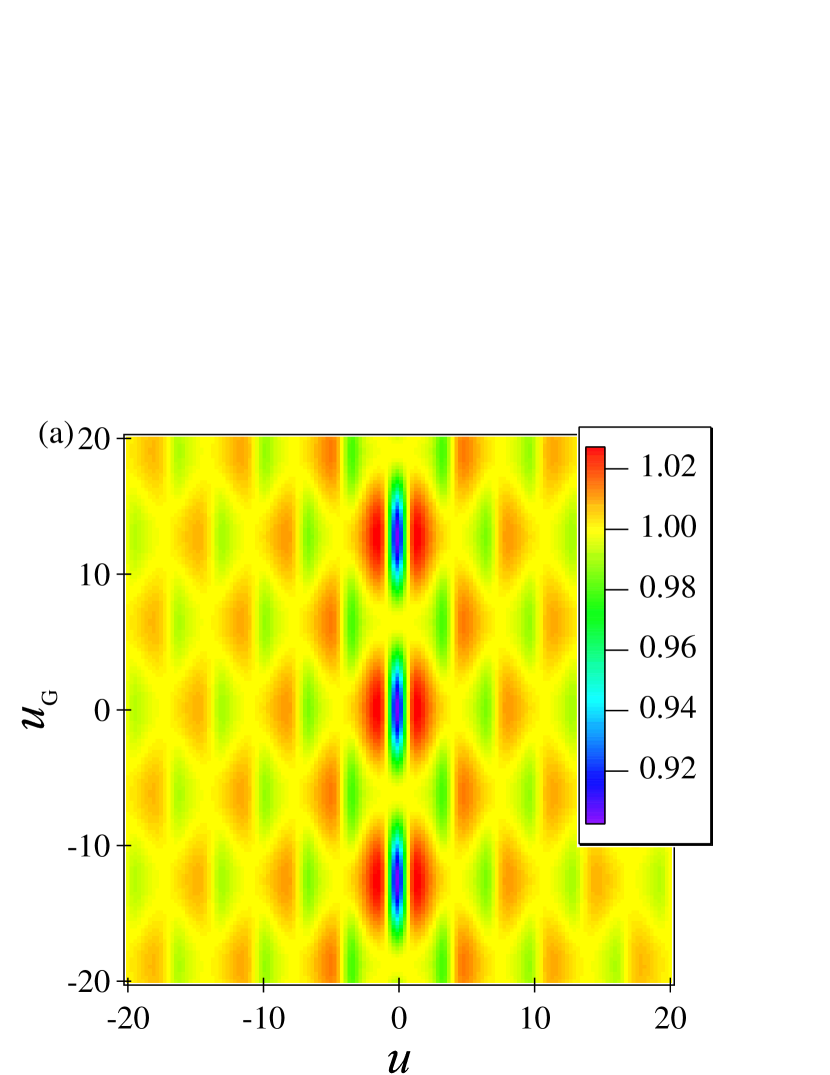
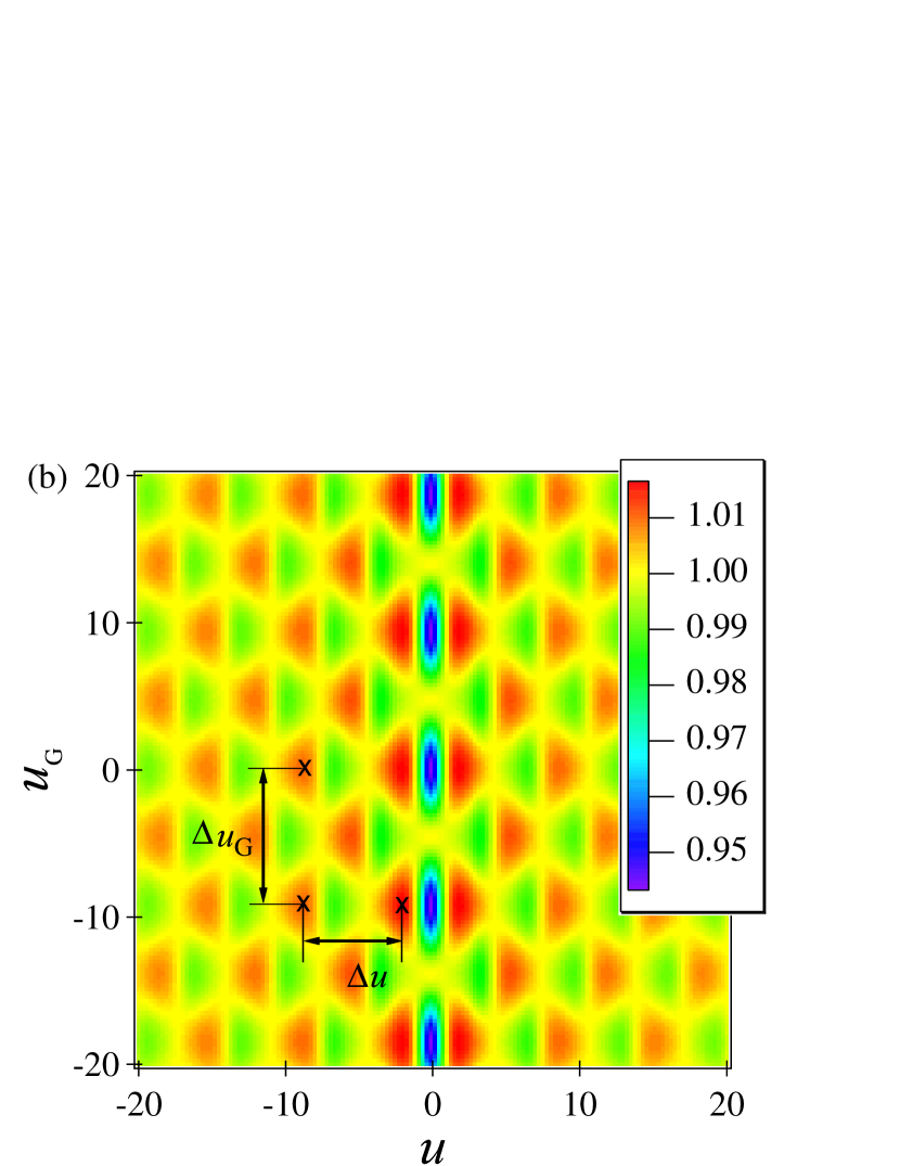
Fig. 5 as a function of the source-drain bias for various values of the interaction parameter . Besides the power-law suppression of the amplitude at high applied bias, we see that for strong interaction () the sinusoidal behavior of the oscillations is deformed into a saw-tooth-like shape. Furthermore, although the total current (26) in the presence of contact resistances is always smaller than the current of an ideally contacted wire (), the differential conductance may exceed . This is a well known effect of non-linear transport in Luttinger liquidsFLS:95 , reflecting the fact that the conductance cannot be expressed in terms of single-particle transmission coefficients. In Sec. V we shall comment on how the two types of oscillations may be experimentally distinguished in a three-terminal set-up.
Further interesting insights emerge from the analysis
of the conductance as a function of both the
source-drain bias and the gate
bias . Corresponding conductance plots are shown in Fig. 6. Panels (a), (b) and (c) refer to three different values of the interaction
strength , in the case of a symmetrically applied
source-drain bias, . The oscillations of the conductance as a function of and
are characterized by two periods and . The period coincides with the period of the function [Eq. (53)] appearing in the coherent terms (51) and (52), since the functions and related to the incoherent contribution (50) exhibit
the period . We thus recover the result of Ref. recher-PRB, . On the other hand, the
period in the gate voltage is determined
by the sinusoidal factors of Eqs. (51) and (52).
The values of and depend on the
interaction strength and are inversely proportional
to and , respectively. Interestingly, the ratio of these
periods yields the Luttinger liquid interaction strength, , as can be checked
from the table associated with Fig. 6.
Panel (d) describes the case of an asymmetrically applied bias ( and
), for the same interaction strength as panel (b). In this case [see Eq.(32)], so that an additional dependence on arises from the sinusoidal factors of Eqs. (51) and (52), and the period in at fixed changes. For this reason the two-dimensional pattern of the nonlinear conductance is twisted with respect to panel (b). However, the quantities and related to a symmetrically applied bias can still be obtained, e.g., by projecting the conductance maxima on the -axis and measuring the distance between these projections as indicated by the arrows in panel (d). The value of can therefore be extracted also in this case as . We remark that a qualitatively similar twist of the conductance pattern has recently been observed in carbon nanotubes.hakonen:2007
Conductance plots as a function of the transport and gate voltages have previously been discussed in the context of carbon nanotubes in
Refs. NW-15, and recher-PRB, . We point out that the way we introduce the bias and gate voltages in our model [see Eq. (6)] differs from the one adopted in the above papers. Our approach accounts for several basic physical facts. In a non-chiral quantum wire only the electrochemical potentials of the leads can be controlled experimentally, whereas the electrochemical potentials of right and left movers inside the wire are a result of the biasing of the wire and its screening properties. As a consequence, the source and drain biases, and , are applied here only in the related leads. This is in accord with a basic hypothesis
underlying the definition of an electrode, namely that inelastic processes in the lead
equilibrate absorbed electrons, yielding a voltage drop at the
contacts even in the absence of contact impurities.
On the other hand, the charge density of metallic electrodes is typically insensitive to a gate, due to their electroneutrality. For this reason, in our model the gate voltage is applied only to the interacting wire and not to the leads.
The precise form of the coupling to the biasing voltages adopted in the model has implications on the
behavior of the current as a function of bias and gate voltages. We find that the
dependence on and involves a factor , as shown, for instance, in Eqs. (51) and (52).
[In the dimensionless formulation
one factor of is contained in the definition of the
dimensionless quantities and .] The difference is proportional to the bare electron charge injected into the wire, whereas the factor originates from the partial
screening occurring in a Luttinger
liquid,Egger-Grabert-electroneutrality and physically describes the fraction of the bare charge that remains unscreened. In particular, in the limit of an electroneutral wire we obtain that the
current depends only on the difference and is independent of the gate, as it should be.
On a more formal level, these physical properties are encoded in the zero modes [see Eq. (LABEL:zero-mode)]. Indeed, the transformation of the chiral boson fields gauges away the bias term (6). We note that, differently from the homogenous Luttinger liquid case, in the presence of leads the zero modes cannot be just linear functions of the position uniformly along the entire system. The inhomogeneity of the system leads to a non-trivial space dependence of the zero modes , which can be obtained from the boson Green function of the inhomogeneous LL model, as shown in Eq. (123).
IV.2 Interaction effects on electron tunneling from the tip: The case of adiabatic contacts
We shall now consider the full three-terminal set-up, and discuss the effects of the wire electron-electron interaction on tunneling from the tip, both for the case of electron injection and in the voltage probe configuration. We start by presenting results for a wire with adiabatic contacts (). For a non-interacting wire, the calculation described in Sec. III yields
| (54) |
and
where is the total tunneling strength defined in Eq. (34) and is the tunneling asymmetry parameter introduced in Eq. (35). Thus, in the absence of interaction, the currents depend linearly on the three applied voltages and are independent of the position of the tip.
When electron-electron interaction is taken into account, an exact solution of the tunneling problem is not possible for arbitrary values of the tunneling amplitudes . We shall assume that , consistent with the tunnel Hamiltonian approach, and provide results to leading order in perturbation theory. The currents in the source and drain leads are again written as in Eqs. (16) and (17), where and are evaluated now to order yielding
| (56) |
and
| (57) |
where
| (58) |
Here
| (59) |
is the tunneling amplitude renormalized by the electron-electron interaction. The dimensionless currents read
| (60) |
where
Here is a small dimensionless cutoff parameter for the tip defined in App. B. The functions and are the real and imaginary parts of the auto-correlation function of the chiral wire field defined in Eqs. (143) and (144), respectively, while and are the real and imaginary parts of the correlator of the tip field given in Eqs. (147) and (148). The integral (60) is a cut-off independent quantity.
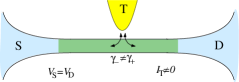
We consider two parameter domains of the three-terminal set-up corresponding to the cases where the tip operates as an electron injector and as voltage probe, respectively. In the electron injection case, source and drain are at the same electrochemical potential while a bias is applied to the tip. For this configuration the current noise was evaluated in Refs. martin:2003, and martin:2005, . Here we shall explicitly evaluate the non-linear tunneling conductances
| (62) |
and
| (63) |
Conventional Luttinger liquid theory, where the presence of the source and drain electrodes is neglected, predicts that an electron charge injected by tunneling e.g. as a right-mover into an interacting wire breaks up into separate charge pulses moving in opposite directions, namely a fraction moving to the right and a fraction going to the left.Safi:1997 ; pham ; martin:2005 ; yacoby-lehur ; lehur ; fisher-glazman This effect originates from the coupling between the densities of right and left moving electrons, accounted for by the homogeneous LL Hamiltonian. As a consequence, one expects that when the tip injects electrons asymmetrically, e.g. only toward the drain electrode on the right (), the electron-electron interaction would cause a part of the current to flow also to the source electrode on the left.
However, when the source and drain electrodes are explicitly taken into account, our results show that the above expectation is in fact wrong. Remarkably, using Eq. (60), one can indeed prove that for the equality
| (64) |
holds, indicating that for a clean wire the current asymmetry is independent of the wire interaction strength . In particular, for fully asymmetric tunneling (), the whole current is injected into the drain electrode, just as in the non-interacting case. This unidirectional charge flow even in the presence of interaction arises from the phenomenon of Andreev-type reflections.safi-schulz ; maslov-stone Even though charge fractionalization occurs in the bulk of the wire, the plasmonic excitations reaching an interface with the leads experience the mismatch of the interaction strengths in the wire and in the electrode and are thus partly reflected as an oppositely charged excitation. The sum of all reflected pulses at both interfaces restores the property that the whole current flows into the drain, like in the non-interacting wire. This behavior is in fact very similar to an effect occurring in a two-terminal set-up, where the conductance of a wire adiabatically connected to electrodes is , independent of the interaction strength. Thus, for perfectly transmitting contacts, it is impossible to extract the interaction constant neither from the conductance of a two-terminal set-up nor from the current asymmetry in three-terminal measurements.
Nevertheless, in a three-terminal set-up signatures of interaction
do appear in the behavior of the differential conductances
and as a function of the tip-source
and tip-drain bias. Figures 7(a) and
7(b) show and for the
case of a tip located in the middle of a wire with interaction
strength . The various curves correspond to different
values of the asymmetry parameter , which unbalances the
amount of injected right vs. left moving electrons. The
fully symmetric case () was discussed in
Ref. nazarov:1997, . While for a non-interacting wire
and are constant [as can easily be
seen from Eqs. (54) and
(IV.2)], in the presence of interaction an
oscillatory behavior arises. These oscillations are entirely due
to the electron-electron interaction in the wire, which causes
Andreev-type reflections even at adiabatic contacts. With
increasing the conductance decreases until
it vanishes for , whereas the conductance
increases up to the maximum value for the completely asymmetric
case. The relation
between these two conductances is independent of .
Figures 7(c) and 7(d) describe
the case of an off-centered tip located at .
Apparently, the period of the oscillations is the same as in
panels (a) and (b) where the tip is in the middle. This is due to
the fact that this period is related to the traversal time of
plasmonic excitations originating from the tip and interfering at
the same point after an even number of Andreev-type reflections
at the contacts. This traversal time depends neither on
nor on the asymmetry coefficient.
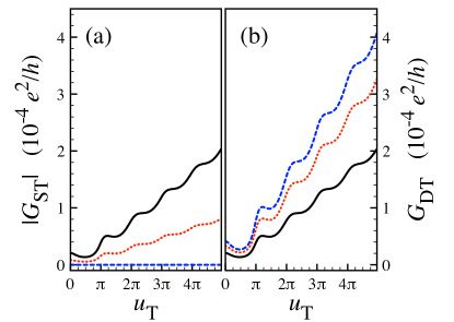
Let us now discuss the configuration where the tip acts as a voltage probe, i.e. when and is set to a value such that is fulfilled. In this configuration the quantity on the left hand side of Eq. (36) is vanishing, due to Eqs. (16) and (17). By applying a source-drain bias, one can analyze how the source-drain conductance
| (65) |
is affected by the interaction strength. It is worth emphasizing that in a two-terminal set-up, i.e. in the absence of the tip (), one obtains for a clean wire , independent of the interaction strength. As already mentioned previously, this is due to the fact that, although the electron charge injected by the source splits up in fractions through the interaction-induced Andreev-type reflections at the contacts, in a clean wire the series of these fractions always sums up to , disguising the interaction effects in the dc average current.safi-schulz Our results show that a quite different behavior emerges for a three-terminal set-up, even in the configuration where the tip does not inject any net current into the wire. Figure 8(a) shows as a function of the source-drain bias, for different values of the interaction strength, ranging from a non-interacting to a strongly interacting wire. The left panel refers to the case of symmetric tunneling , whereas the right one analyzes the role of a tunneling asymmetry. As one can see, the effects of interaction in the wire become observable through the voltage probe, since oscillation of originating from Andreev-type reflections emerge. Notice that at constant bare tunneling amplitude the zero bias conductance is higher in the presence of interaction than for a non-interacting wire, since the renormalization (59) of the tunneling amplitude suppresses . With increasing tunneling asymmetry [see Fig. 8(b)], the differences between interacting and non-interacting wires become less pronounced, and indeed the oscillations are washed out for fully asymmetric tunneling .

The dimensionless tip voltage
ensuring =0 shows an interesting dependence on the
source-drain bias. In the limiting cases of symmetric and
completely asymmetric tunneling this dependence coincides for
interacting and non-interacting wires (namely for
and for ). For
intermediate values of the asymmetry parameter the tip
voltage shows an oscillatory behavior with period as a function of the source-drain bias. We also
see that the period of in
Fig. 8 is twice as large as the period of
and in Fig. 7 where the tip is in the
electron injection configuration. This is due to the fact that in
Fig. 8 the source-drain bias is applied
symmetrically () while in Fig. 7
source and drain are both grounded and the bias is only applied to the tip.
Finally, we emphasize again the difference between the electron
injection and the voltage probe configurations of the tip: While
in the former case an asymmetry in tunneling does not spoil the
observation of effects of electron-electron interaction (see
Fig. 7), in the latter case interaction-induced
oscillations can be best observed for symmetric tunneling and
they are in fact vanishing for fully asymmetric tunneling.
IV.3 Interaction effects on electron tunneling from the tip: The case of a wire with non-ideal contacts
In this section we analyze the three-terminal transport properties in the presence of electron-electron interaction, contact impurity scattering and electron tunneling from the tip. In particular, we discuss how a finite contact resistance modifies the Andreev-type oscillations of the tunneling conductances, previously discussed for the case of adiabatic contacts (). We present results obtained by perturbation theory for weak contact impurities , and tunneling amplitudes . Technical details can be found in the Appendices. The currents may be written as
| (66) |
and
| (67) |
Here is the current of an ideally contacted wire in the absence of the tip, whereas is the leading order term accounting for non-ideal contacts [see Eq. (45)]. In general, this latter term involves both Fabry-Pérot and Andreev-type oscillations. Both, and , vanish when the electrochemical potentials for source and drain electrodes are equal (); alternatively, they can be easily determined by measuring the current-voltage characteristics in the absence of the tip. Henceforth, we shall focus on contributions to the currents arising from the presence of the tip. The leading order terms and , given by Eq. (58), describe tunneling into an ideally contacted wire and contain only Andreev-type oscillations. The next-to-leading order terms (, , …) also exhibit oscillations originating from interference between backscattering at the contacts and tunneling to/from the tip. Such oscillations, though modified by the interaction, are already present in a non-interacting wire, unlike the Andreev-type oscillations of the leading order terms (), that are instead entirely due to the interaction. We thus analyze how interaction affects the terms , which represent the most relevant correction to the Andreev-type oscillations discussed above. These terms describe to leading order the interplay between electron injection at the tip and backscattering at the S and D contacts.

Explicitly one finds
| (68) |
where , and
| (69) |
where
| (70) | ||||
| (71) |
The functions
and are defined in
App. B in Eqs. (B) and (133), respectively,
and the functions ,
,
and , accounting for the real and the imaginary
parts of several correlation functions in the wire and in the tip, are
defined in App. C in Eqs. (C), (138), (147) and (148), respectively.
For simplicity, we limit the analysis of Eqs. (68) and (69) to the electron injection configuration where source and drain are grounded. We start with the case of symmetric tunneling ().
As already observed in Sec. III for a noninteracting wire,
the term (68) leads to additional oscillations in the
differential conductance of the three-terminal set-up. These
conventional oscillations are characterized by two periods
related to the distances between the tip and the contact
impurities, so that the pattern depends on the tip position.
Electron-electron interaction modifies this pattern reducing the
amplitude of the conventional oscillations and giving rise to
additional Andreev-type oscillations. The case of a tip in the
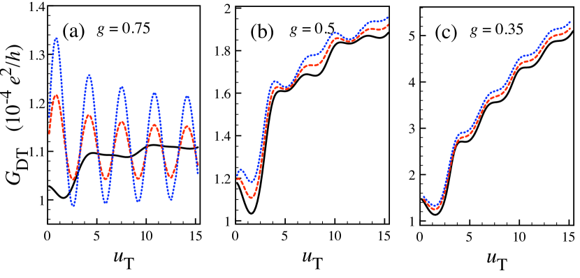
middle of the wire is shown in the upper panels (a), (b) and (c) of Fig. 9, where the
differential conductance is plotted as a function of
the tip bias for three different values of interaction
strength, ranging from weak (), over moderate ()
to strong interaction (), as displayed in the three
panels. In each panel the solid curve refers to the case of ideal
contacts where the oscillations are purely of Andreev-type. The
dotted and dashed curves describe the effect of finite contact
resistances arising from the contribution of the term
(68). As one can see from panel (a), for weak
electron-electron interaction the conventional oscillations
dominate and mask the Andreev-type oscillations. In this case,
only extremely good contacting might allow to identify
Andreev-type processes. However, for moderate interaction strength
[panel (b)], the two types of oscillations have comparable amplitudes, and for strong interaction [panel (c)] the
conventional oscillations are strongly suppressed while the term (68) only causes a small shift of the conductance value. The
oscillations of are essentially Andreev-type.
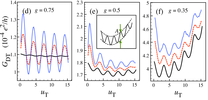
A similar effects occurs when the tip is closer to one of the
contacts displayed in the lower panels (d), (e) and (f) of Fig. 9. The main difference is that in this case the pattern of
the Andreev-type oscillations is more sinusoidal, even for weak interactions.
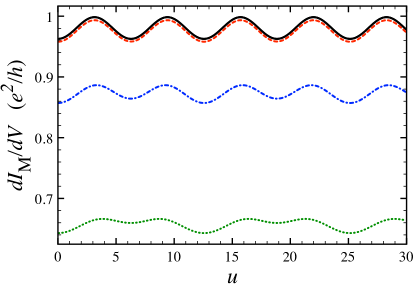
Our result indicates that, for a wire with a given interaction strength, there is crossover value of the (renormalized) contact resistance, below which the oscillations of the non-linear conductance can essentially be attributed to Andreev-type processes. We have quantified for the case of a tip close to the contacts, where the regularity of oscillations allows for a straightforward determination of their amplitude, defined as the average distance between maxima and minima, as schematically displayed in the inset of Fig. 9(e). The crossover impurity strength is then simply determined by the value of for which the amplitude of the conventional oscillation term [see Eq. (68)] equals the amplitude of the Andreev-type oscillation term [see Eq. (58)]. The result is given in Table 1 for different values of interaction strength. For contact impurity strength the oscillations of the non-linear conductance are essentially of Andreev-type.
| 0.4 | 0.5 | 0.6 | 0.7 | 0.8 | |
|---|---|---|---|---|---|
| 0.2 | 0.02 |
Let us finally briefly consider the case of asymmetric tunneling . An important result is that, in view of Eq. (68), the contribution to the current of order vanishes in the case of totally asymmetric tunneling (). This property is thus robust to electron-electron interaction within the Luttinger liquid picture. In fact, one can show that in this case only perturbative contributions of order () are nonvanishing.
V Discussion and Conclusions
In the present work, we have investigated transport
properties of a quantum wire contacted to source and drain
reservoirs in the presence of a third electrode (tip) injecting
electrons into the wire. We have tailored our model to account for
various aspects of a typical experimental situation by
including finite contact resistances and the presence of a gate in
addition to electron-electron interaction, and by analyzing the
effect of the position of the tip as well as the role of a
tunneling asymmetry. Specifically, we have considered both the
situation where the tip behaves as an electron injector and the
voltage probe configuration. We have found that the three-terminal
set-up exhibits extremely rich behaviors, determined not
only by each of the above aspects, but also by their interplay. In
order to facilitate the discussion, we propose to the reader
different perspectives from which our results can be considered.
The effects of electron-electron interaction on Fabry-Pérot oscillations.
The origin of Fabry-Pérot oscillations boils down to quantum
interference between electron backscattering at two (or more)
impurities. As a consequence, this phenomenon is
present also in a non-interacting quantum wire (see Sec. III), where the oscillations appear both as a function of the source-drain bias and as a function of the gate voltage. The interference pattern is
modified by electron-electron interaction, which introduces a power-law suppression of the amplitude and, especially for , deforms the sinusoidal shape towards a saw-tooth-like shape (see Fig. 5).
Interaction also leads to a (partial) screening of the charge in the wireEgger-Grabert-electroneutrality , causing a change of
the oscillation period as a function of the gate bias
with respect to the period as a function of the source-drain bias. This effect suggests an operative procedure to extract the Luttinger liquid parameter from measurements of the non-linear conductance in the Fabry-Pérot regime (see
Fig. 6). The effects of an asymmetrically applied source-drain bias have also been discussed. We emphasize that, differently from previous approaches adopted in the literature, our way to introduce the biasing voltages correctly recovers both gauge invariancebuttiker:1993 and the property that, in the limit of strong interaction , the current-voltage characteristics only depends on the difference between source and drain bias .
Conventional vs. Andreev-type oscillations. Besides modifying Fabry-Pérot oscillations, electron-electron interaction also yields another major effect, which is absent in a non-interacting wire: At the wire-electrode interfaces, plasmon excitations are partially reflected due to the mismatch of interaction strengths in the interacting wire and the non-interacting electrodes. This effect, entirely due to interaction, occurs also for ideally contacted adiabatic interfaces and gives rise to a different type of oscillations, which are termed Andreev-type oscillationsNW-14 since the incoming charge and the fractional charge reflected at the contact have opposite signs, just as at an interface between a normal metal and a superconductor. In real experiments with interacting quantum wires in the Fabry-Pérot regime, the current-voltage characteristics will in general exhibit both conventional Fabry-Pérot oscillations, i.e. oscillations that are already present in a non-interacting wire and that are simply modified by interaction, and Andreev-type oscillations, purely originating from interaction. The interesting question arises whether one can distinguish between these two oscillatory phenomena in an operative way and, in particular, whether it is possible to determine regimes and conditions, under which the latter can be observed.
Since the amplitude of Fabry-Pérot oscillations is roughly proportional to the reflection coefficients of the contacts whereas Andreev-type processes occur even with ideal interfaces, one might at first think that with improving transparency of the contacts the non-linear conductance of a two-terminal set-up would exhibit a predominance of Andreev-type oscillations over the conventional Fabry-Pérot ones. This is, however, not the case, since for an ideally contacted wire the sum of all Andreev-type reflection processes at the two interfaces exactly recovers the injected pulse, when the sign of all reflected charge pulses is taken into account. The transmission of an interacting wire adiabatically connected to non-interacting leads turns out to equal 1, as was pointed out in Refs. safi-schulz, and maslov-stone, . Although Andreev-type oscillations of the conductance do appear in the presence of even a single impurityNW-14 , their amplitude is proportional to the impurity reflection coefficient. This implies that two-terminal set-ups are not suitable to distinguish between Andreev-type and Fabry-Pérot oscillations, since both oscillations have the same dependence on the impurity strengths . Furthermore they also exhibit the same period as a function of the source-drain bias.
In contrast, our analysis suggests that a three-terminal set-up may allow one to distinguish Andreev-type oscillations from conventional oscillations. As far as Andreev-type oscillations are concerned, three-terminal set-ups indeed offer one important advantage with respect to two-terminal ones: in the presence of a third electrode, Andreev-type oscillations appear even for the ideal case of a wire adiabatically connected to the source and drain electrodes (=0). In the presence of interaction the tip-source and tip-drain non-linear conductances and oscillate as a function of the tip voltage already to leading order in the tunneling amplitude, independent of contact impurity strengths . This effects holds when the tip acts as an electron injector (see Fig. 7) as well as when it acts as a voltage probe (see Fig. 8), and the oscillations vanish for a non-interacting wire [see Eqs. (54) and (IV.2)]. Thus, quite differently from a two-terminal set-up, in three-terminal set-ups Andreev-type oscillations become better visible when the contact transparency is improved.
In view of the fact that in realistic experiments the contact
resistance is always finite, we have quantitatively evaluated the
influence of the contact resistance on the conductance oscillations [see
Eq.(69)] showing that additional Fabry-Pérot-type
oscillations superimpose with the Andreev-type ones (see
Fig.9). We have thus put forward criteria for
observing the interaction induced Andreev-type oscillations. At
least two experimental situations are promising: For the
conventional case of symmetric tunneling form the tip, we have
determined typical values of the contact resistance below which
the oscillations in the current-voltage characteristics can
essentially be attributed to Andreev-type phenomena. The result,
shown in Table 1, indicates that the stronger the
interaction of the wire the larger are the contact resistances
that are tolerable to still observe Andreev-type oscillations.
Furthermore, in case that the set-up allows for fully asymmetric
tunneling, the leading order correction (69)
competing with the Andreev-type term is vanishing, even in
the presence of interaction.
In summary, in systems like carbon nanotubes where the interaction
strength is typically strong, , while
electron injection from an STM tip is typically symmetric,
Andreev-type oscillations may be observed by achieving a high
quality of the contacts to the leads. In contrast, in
semiconductor quantum wires, where the interaction strength is
usually moderate , asymmetric tunneling induced
by a magnetic field is more suitable to observe
Andreev-type oscillations.
The effects of asymmetric tunneling. The above-mentioned case of asymmetric tunneling deserves some further remarks. Recent experiments by Yacoby and co-workersyacoby ; yacoby:2 have shown that fully asymmetric tunneling into semiconductor-based quantum wires can be realized by appropriate tuning of a magnetic field. Inspired by these experiments, we have considered the possibility of an asymmetry in electron tunneling from the tip. Before discussing our results we would like to point out the relation between our model and Yacoby’s experimental set-up. While Yacoby et al. study electron tunneling between two parallel wires where momentum conservation is required, our model considers injection from a point-like tip. Although these two situations may at first seem incompatible, a regime can be determined where they are equivalent. In the experiments of Refs. yacoby, ; yacoby:2, electrons are injected from an upper shorter wire with length into a lower longer wire with length . Since the tunneling region reasonably coincides with the length of the short wire, momentum conservation only holds up to an uncertainty . Although this uncertainty is small enough to select a specific electron momentum state in the upper wire, may be much bigger than the mean level spacing of the lower wire, if the latter is much longer than the former (). In this regime, while the electron wave function behaves like a plane wave for the short wire, for the long wire it can effectively be considered as a localized wave packet, and our model applies.
Under these conditions several interesting effects emerge. In the first instance, by using the tip as an electron injector, the tunneling asymmetry can be exploited to gain the transmission coefficient of each contact by measuring the current asymmetry (36) in the two cases of tunneling purely to the right () and to the left (), as has been shown in Eq. (40). Secondly, when the tip is used in the configuration of a voltage probe, fully asymmetric tunnelling allows to eliminate the suppression of the source-drain conductance , which occurs for symmetric tunneling. Similarly, becomes independent of the tip position.
When electron-electron interaction is taken into account, the scenario is even richer. Luttinger liquid theory predicts that electron-electron interaction induces a current asymmetry which depends on the interaction strength . The appealing question arises whether this effect is observable in experiments, where currents are measured not directly in the interacting wire but in metallic electrodes connected to it. The investigation carried out in Ref. yacoby-lehur, , based on the assumption that the interfaces between the interacting wire and the electrodes can be treated phenomenologically with a transmission coefficient à la Landauer-Büttiker, has led these authors to the claim that the interaction strength can be observed via the current asymmetry. Here we have scrutinized this prediction by taking the presence of source and drain electrodes into account fully consistently within the inhomogeneous Luttinger liquid model. Considering as a test bench the case of a wire adiabatically contacted to source and drain electrodes, we have proven that, although charge fractionalization does occur in the bulk of the wire, the sum of Andreev-type reflection processes at the contacts leads to a current asymmetry that is independent of the electron-electron interaction strength, just as it is the case with the two terminal conductance . Thus, already for this ideal case, no proof of charge fractionalization can be gained from the analysis of , or from the ration . We have also shown that, nevertheless, interaction effects do appear in the behavior of the nonlinear conductance, where interaction induced oscillations arise as a function of the tip-source and tip-drain bias. It is worth emphasizing that this feature is due to the three-terminal set-up, since the two-terminal conductance of a Luttinger liquid ideally contacted to leads is independent of the source-drain bias.
Acknowledgements.
The authors acknowledge stimulating discussions with R. Fazio, T. Martin, P. Recher, and B. Trauzettel, and computational support by D. Passerone. Funding was provided by the Deutsche Forschungsgemeinschaft (DFG), by the NANOFRIDGE EU Project, by the “Rientro dei Cervelli” MIUR Program, as well as by the Italian-German collaboration program Vigoni.Appendix A Keldysh formalism and perturbative evaluation of the current
In order to compute the current in the three terminal set-up, we adopt the Keldysh formalism,KEL suitable to account for out-of-equilibrium properties. According to Eq. (LABEL:I-W), the current at position (located in the source or in drain leads) and time can be written as
| (72) |
where
| (73) |
Here () corresponds to the upper (lower) branch of the Keldysh contour depicted in Fig. 10. The current and various other quantities introduced below also depend on the injection point and the impurity positions and . These variables will frequently be suppressed to simplify notation.
In the Keldysh interaction picture with
| (74) |
and
| (75) |
one obtains
where denotes the average with respect to the equilibrium state determined by the Hamiltonian , and is the Keldysh time-ordering operator. Expanding the exponent in Eq. (LABEL:I-prel) perturbatively in terms of and , one obtains the current to the desired order. Below we sketch the calculation of , i.e., the contribution of order to . With the abbreviations
| (77) |
one obtainsNOTA-G2L
| (78) | |||||
where we have used the properties
| (79) |
and
| (80) |
Since the electron-electron interaction (8) contains only forward scattering terms, all non-vanishing wire correlation functions must involve an even number of operators with a given chirality . This yields , so that
The term with can be shown to yield the same contribution as the term with . To see this explicitly, one makes use of , exploits Eqs. (79) and (80), and renames variables according to , () and . One can then write
where
| (83) |
contains correlation functions of wire operators, while
| (84) |
is a correlation function of the tip. These correlation functions are evaluated in App. B starting with Eq. (LABEL:W-G2L-prel) and (132), respectively. Inserting these results, one obtains
where, for any pair of bosonic operators and , the following definitions hold
| (86) | ||||
| (87) | ||||
| (88) |
We now observe that the last term in Eq. (A) can be dropped. Indeed, since it depends neither on nor on (), it can be singled out of the sums and integrals ; the remaining sums and integrations yield a vanishing result, since the corresponding expression equals the term of order of an expansion of
| (89) |
Simple transformations of the integration variables of Eq. (A), and use of the relations
| (90) | |||||
| (91) |
obtained from the correlation functions provided in App. C, yield
Taking into account Eqs. (B), (B), (133), and (135), we now observe that upon reversal of Keldysh contour indices (),
| (93) | |||||
| (94) | |||||
| (95) | |||||
| (96) |
implying that in Eq. (A) the contribution for is conjugate to the one stemming from . Thus
The term appearing in the last line is
positive (negative) for a measurement point located in the
drain (source) lead. Recalling that the current can be written as
in Eqs. (16), (17), it is easily seen that
those terms that are multiplied by yield
, whereas the other ones yield . Inserting
Eqs. (B), (B), (133), and
(135) into Eq. (A), and changing to
dimensionless integration variables , the
result (69) is obtained.
Similar procedures can be applied to evaluate the terms of order , and . We find
| (98) |
| (99) |
and
| (100) |
where
| (101) |
| (102) |
and
| (103) |
Appendix B Evaluation of and -factors by Bosonization
The Hamiltonian (74) of the interaction picture decomposes into commuting wire and tip parts, i.e., . For a non-interacting wire , and the wire correlation functions introduced in Eqs. (83), (101), (102) and (103) can be factorized into products of single-particle electron correlators using Wick’s theorem. In this case the W’s can be evaluated straightforwardly, and the results for the contributions (A), (98), (99) and (100) to the current coincide with the corresponding terms of an expansion of the current obtained from the scattering matrix formalism. In the interacting case, however, , and Wick’s theorem cannot be applied. In this appendix we evaluate the wire correlators W using the bosonization technique.BOS The wire field operators can be represented as
| (104) |
where the fields describe particle-hole excitations,
and are Klein factors represented as Majorana
fermions.BOS Finally, is a cut-off length of order
the lattice spacing.
Introducing Eq. (104) into Eqs. (3) and
(13), one obtains
| (105) |
where and are conjugate bosonic fields, i.e., . Finally,
| (106) |
is the inhomogeneous interaction parameter. Notice that , where describes the non-interacting case present in the leads. The limit corresponds to strongly repulsive interaction. The wire current operator Eq. (LABEL:I-W) is expressed in terms of the dual field as
| (107) |
Further, with the help of the relation
| (108) |
the term (6) of the Hamiltonian can be written as
| (109) |
We start by discussing the derivation of . Inserting Eqs. (104), (107) and (108) into Eq. (A), one obtains
Here
accounts for the correlation function of fermionic Klein factors, whereas
| (112) | |||||||
correlates bosonic vertex operators. Also, we have introduced the notation . The expression (112) can straightforwardly be evaluated taking into account that for a functional
| (113) |
where and are linear combinations of bosonic operators, one hasBOS
| (114) |
Furthermore, it can be shown that , i.e. the first term appearing in the exponent of Eq. (112), simply yields a shift in the operators according to
| (115) |
where the zero modes
| (116) | |||||||
| (122) | |||||||
fulfill the equation
| (123) |
After lengthy but straightforward algebra one obtains
| (124) | |||||||
where
The correlation functions and are defined in App. C [see Eqs. (C) - (142)] and also given explicitly there in the zero temperature limit. The arguments and () are dimensionless time and space variables. In deriving Eqs. (124) and (B) we have used the equalities
| (126) |
and
| (127) | |||||
| (128) | |||||
| (129) |
valid for any pair and of real Bose operators.
As far as the tip correlators are concerned, see Eqs. (84), (100), and (98), Wick’s theorem might be applied, since the tip is supposed to be non-interacting, and the use of bosonization is unnecessary. However, to have a uniform formalism and notation throughout the paper, we prefer to utilize a bosonized approach for the tip as well. The tip electron field and density are written as
| (130) |
and
| (131) |
where is a chiral (right-moving) boson field, and and are the Klein factor and cutoff length of the tip, respectively. By way of example, we evaluate here the T-factor (84) appearing in the calculation of . Inserting Eqs. (130) and (131) into Eqs. (77) and (84), one obtains
| (132) |
where, similar to the wire case,
| (133) |
accounts for the correlation function of fermionic Klein factors, whereas the correlator of bosonic vertex operators reads
| (134) |
It is easily verified that the first term in the exponential function, which originates from the term (12) in the Hamiltonian, merely yields a time-dependent phase factor, so that
| (135) |
where
The functions and are given in App. C, see Eqs. (147) and (148).
Appendix C Correlation functions
This appendix collects properties of correlation functions appearing in Eqs. (60) and (69), as well as in Eqs. (B) and (B). The transport properties of the wire are expressed in terms of the functions
| (138) | |||||
where the functions and are the real and imaginary parts, respectively, of the auto-correlation functions of the bosonic fields . Specifically
| (139) | |||||
| (140) |
Likewise, the real and imaginary parts of the cross-correlation functions of fields with different chirality read
| (141) | |||
| (142) |
Notice that the real part of the correlation functions of fields with the same chirality needs to be defined with an infrared regularization as in Eq. (139). The above equations are given in terms of the dimensionless time and space variables and introduced previously. From the inhomogeneous Luttinger liquid model one obtains at zero temperature
| (143) |
| (144) |
and
and
Here we have introduced , , and the dimensionless cutoff length , as well as the Andreev-type reflection coefficient .
The correlation functions for the non-interacting tip can directly be obtained from the above results. The tip is described by a single chiral mode, and we need the correlation function only for coordinates at the injection point . From Eqs. (143) and (144) we find for by taking the limit and replacing by
| (147) | |||||
| (148) |
References
- (1) Z. Zhang, and C. M. Lieber, Appl. Phys. Lett. 62, 2792 (1993); J. W. G. Wildör, L. C. Venema, A.G. Rinzler, R. E. Smalley, and C. Dekker, Nature 391, 59 (1998); T. W. Odom, J.-L. Huang, P. Kim, and C. M. Lieber, ibid. 391, 62 (1998); M. A. Topinka, B. J. LeRoy, S. E. J. Shaw, E. J. Heller, R. M. Westervelt, K. D. Maranowski, and A. C. Gossard, Science 289, 2323 (2000); B.J. LeRoy, I. Heller, V. K. Pahilwani, C. Dekker, and S. G. Lemay, Nano Lett. 7, 3138 (2007).
- (2) A. Yazdani, B. A. Jones, C. P. Lutz, M. F. Crommie, and D. M. Eigler, Science 275, 1767 (1997); S. H. Pan, E. W. Hudson, and J. C. Davis, Appl. Phys. Lett. 73, 2992 (1998); T. Proslier, A. Kohen, Y. Noat, T. Cren, D. Roditchev, and W. Sacks, Europhys. Lett. 73, 962 (2006); A. Kohen, Th. Proslier, T. Cren, Y. Noat, W. Sacks, H. Berger, D. Roditchev, Phys. Rev. Lett. 97, 27001 (2006).
- (3) B. J. van Wees, K.-M. H. Lenssen, and C. J. P. M. Harmans, Phys. Rev. B 44, 470 (1991); A. F. Volkov, Phys. Rev. Lett. 74, 4730 (1995); F. K. Wilhelm, G. Schön, and A. D. Zaikin, Phys. Rev. Lett. 81, 1682, (1998); J. J. A. Baselmans, A. F. Morpurgo, B. J. van Wees, and T. M. Klapwijk, Nature 397, 43 (1999); P. Samuelsson, J. Lantz, V. S. Shumeiko, and G. Wendin, Phys. Rev. B 62, 1319 (2000); F. Giazotto, T. T. Heikkilä, A. Luukanen, A. M. Savin, and J. P. Pekola, Rev. Mod. Phys. 78, 217 (2006).
- (4) M. Woodside, and P. McEuen, Science 296, 1098 (2002).
- (5) A. Naik, O. Buu, M. D. LaHaye, A. D. Armour, A. A. Clerk, M. P. Blencowe, and K. C. Schwab, Nature 443, 193 (2006); R. Ruskov, K. Schwab, and A. N. Korotkov, Phys. Rev. B 71, 235407 (2005).
- (6) M. Büttiker, Y. Imry, and M. Ya. Azbel, Phys. Rev. A, 30, 1982 (1984); F. Marquardt, and C. Bruder, Phys. Rev. B 70, 125305 (2004); F. Marquardt, Phys. Rev. B 74, 125319 (2006).
- (7) C. Texier, and M. Büttiker, Phys. Rev. B 62, 7454 (2000); S. Pilgram, P. Samuelsson, H. Förster, and M. Büttiker, Phys. Rev. Lett. 97, 066801 (2006); H. Förster, P. Samuelsson and M. Büttiker, New J. Phys. 9, 117 (2007).
- (8) A. Yacoby, H.L. Stormer, K.W. Baldwin, L.N. Pfeiffer, and K.W. West, Solid State Comm. 101, 77 (1997); R. de Picciotto, H.L. Stormer, L.N. Pfeiffer, K.W. Baldwin, and K.W. West, Nature 411, 51 (2001).
- (9) C. T. White, and T. N. Torodov, Nature 393, 240 (1998).
- (10) W. Liang, M. Bockrath, D. Bozovic, J. H. Hafner, M. Tinkham, H. Park, Nature 411, 665 (2001).
- (11) A. Yacoby, H. L. Stormer, N. S. Wingreen, L. N. Pfeiffer, K. W. Baldwin, and K. W. West, Phys. Rev. Lett. 77, 4612 (1996); O. M. Auslaender, A. Yacoby, R. de Picciotto, K. W. Baldwin, L. N. Pfeiffer, and K. W. West, Phys. Rev. Lett. 84, 1764 (2000).
- (12) O. M. Auslaender, H. Steinberg, A. Yacoby, Y. Tserkovnyak, B. I. Halperin, K. W. Baldwin, L. N. Pfeiffer, and K. W. West, Science 308, 88 (2005); H. Steinberg, O. M. Auslaender, A. Yacoby, J. Qian, G. A. Fiete, Y. Tserkovnyak, B. I. Halperin, K. W. Baldwin, L. N. Pfeiffer, and K. W. West, Phys. Rev. B 73, 113307 (2006).
- (13) M. Bockrath, D. H. Cobden, J. Lu, A. G. Rinzler, R. E. Smalley, L. Balents, and P. L. McEuen, Nature 397, 598 (1999); Z. Yao, H. W. Ch. Postma, L. Balents, and C. Dekker, Nature 402, 273 (1999).
- (14) Na Y. Kim, P. Recher, W. D. Oliver, Y. Yamamoto, J. Kong, and H. Dai, Phys. Rev. Lett. 99, 036802 (2007).
- (15) S. Eggert, Phys. Rev. Lett. 84, 4413 (2000).
- (16) I. Ussishkin, and L.I. Glazman, Phys. Rev. Lett. 93, 196403 (2004).
- (17) A. Crépieux, R. Guyon, P. Devillard, and T. Martin, Phys. Rev. B 67, 205408 (2003).
- (18) A. V. Lebedev, A. Crépieux, and T. Martin, Phys. Rev. B 71, 75416 (2005).
- (19) F. Wu, P. Queipo, T. Tsuneta, T. H. Wang, E. Kauppinen, and P. J. Hakonen, Phys. Rev. Lett. 99, 156803 (2007).
- (20) L. G. Herrmann, T. Delattre, P. Morfin, J.-M. Berroir, B. Plaçais, D. C. Glattli, and T. Kontos, Phys. Rev. Lett. 99, 156804 (2007).
- (21) H. Steinberg, G. Barak, A. Yacoby, L. N. Pfeiffer, K. W. West, B. I. Halperin, K. Le Hur, Nature Phys. 4, 116 (2008).
- (22) I. Safi, and H. J. Schulz, Phys. Rev. B 52, R17040 (1995).
- (23) D. L. Maslov, and M. Stone, Phys. Rev. B 52, R5539 (1995); V. V. Ponomarenko, ibid. 52, 8666 (1995).
- (24) Due to the effectively short-ranged interaction induced by the gate, a Wigner crystal regime does not arise in the situation discussed here.
- (25) C. S. Peça, L. Balents, K. J. Wiese, Phys. Rev. B 68, 205423 (2003).
- (26) P. Recher, N. Y. Kim, and Y. Yamamoto, Phys. Rev. B 74, 235438 (2006).
- (27) K. Le Hur, B.I. Halperin, A. Yacoby, Ann. Phys. (New York) 323, 3037 (2008).
- (28) M. Büttiker, J. Phys.: Condensed Matter 5, 9361 (1993).
- (29) Here is taken as an external parameter, and the choice of the value ensures a vanishing average current . The term ’voltage probe’ is sometimes also used in the literature for a terminal where the electrochemical potential dynamically changes to ensure that both the average current and its current fluctuations vanish (see e.g. Ref. [voltage-probe-refs, ]). As far as the results for the average currents in the set-up are concerned, our definition of a voltage probe is equivalent to the latter choice. Differences might emerge for the current fluctuations, which are beyond the topic of the present work.
- (30) L. V. Keldysh, Zh. Eksp. Teor. Fiz. 47, 1515 (1964).
- (31) Note that the renormalization exhibits the same scaling exponent as in the homogeneous Luttinger liquid model (see e.g. C. L. Kane, and M. P. A. Fisher, Phys. Rev. B 46, 15233 (1992)). In the inhomogeneous Luttinger liquid model used here, however, the renormalization flow driven by the relevant impurity backscattering operator is cut not only by a finite temperature or bias , but also by the finite length of the wire . For this reason our perturbative treatment is safe also at and .
- (32) F. Dolcini, H. Grabert, I. Safi, and B. Trauzettel, Phys. Rev. Lett. 91, 266402 (2003); F. Dolcini, B. Trauzettel, I. Safi, and H. Grabert, Phys. Rev. B 71, 165309 (2005).
- (33) P. Fendley, A. W. W. Ludwig, and H. Saleur, Phys. Rev. B 52, 8934 (1995).
- (34) R. Egger and H. Grabert, Phys. Rev. Lett. 79, 3463 (1997).
- (35) I. Safi, Ann. Phys. (Paris) 22, 463 (1997) [in French].
- (36) K.-V. Pham, M. Gabay, and P. Lederer, Phys. Rev. B 61, 16397 (2000); K.-I. Imura, K.-V. Pham, P. Lederer, and F. Piéchon, Phys. Rev. B 66, 035313 (2002).
- (37) K. Le Hur, Phys. Rev. B 65, 233314 (2002) and Phys. Rev. Lett. 95, 076801 (2005).
- (38) see also M. P. A. Fisher, and L. I. Glazman, Transport in a one-dimensional Luttinger liquid, in Mesoscopic Electron Transport, ed. by L. L. Sohn, L. P. Kouwenhoven, and G. Schön, NATO ASI Series E 345, Kluwer Academic Publishers (1997).
- (39) Y. V. Nazarov, A. A. Odintsov, and D. V. Averin, Europhys. Lett. 37, 213 (1997).
- (40) One can prove that only impurity backward scattering contributes to order .
- (41) A. O. Gogolin, A. A. Nersesyan, and A. M. Tsvelik, Bosonization and Strongly Correlated Systems (Cambridge University Press, Cambridge, 1998).