Epitaxial ferromagnetic Fe3Si/Si(111) structures with high-quality hetero-interfaces
Abstract
To develop silicon-based spintronic devices, we have explored high-quality ferromagnetic Fe3Si/silicon (Si) structures. Using low-temperature molecular beam epitaxy at 130 ∘C, we realize epitaxial growth of ferromagnetic Fe3Si layers on Si (111) with keeping an abrupt interface, and the grown Fe3Si layer has the ordered phase. Measurements of magnetic and electrical properties for the Fe3Si/Si(111) yield a magnetic moment of 3.16 /f.u. at room temperature and a rectifying Schottky-diode behavior with the ideality factor of 1.08, respectively.
Semiconductor spintronic devices such as spin-field effect transistors (spin FET) are one of the possible candidates to substitute for existing silicon-based complementary metal-oxide-semiconductor devices.Wolf ; Datta ; Sugahara ; Hall To realize operations of the spin FET, an electrical spin injection from ferromagnets into semiconductors is an essential technology. For III-V semiconductor devices, several groups have demonstrated highly efficient spin injection and detection using an epitaxial Fe thin film and tailored Schottky tunnel barriers so far.Hanbicki ; Hanbicki2 ; Lou From these facts, it is necessary for semiconductor spintronics to develop crystal growth techniques of ferromagnets on semiconductors with keeping high-quality interfaces. In particular, it will become key to build epitaxial growth of ferromagnets on silicon (Si) from the viewpoint of application to existing silicon large-scale integrated circuit (LSI) technologies.Min
Moreover, for spintronics, Si has been regarded as an ideal material because of a long spin relaxation time due to weak spin-orbit interaction, weak hyperfine interaction and lattice inversion symmetry, which will give rise to a long spin diffusion length in the devices. Recently, spin transport in Si conduction channels was experimentally demonstrated although their operations were limited at low temperatures.Appelbaum ; Jonker1 ; Jonker2 This means that the spin degree of freedom can be introduced into Si-based electronic devices.
To date, ferromagnetic MnAs thin films have been grown epitaxially on Si (001),Tanaka but electrical spin injection from MnAs into Si across a Schottky tunnel barrier has never been demonstrated unfortunately. Also, the Curie temperature of MnAs is 315 K,Plake which may be relatively low for an operation temperature of future LSIs. Thus, possibilities of other high-Curie temperature materials compatible with Si should be explored. Here we select a ferromagnetic Heusler alloy Fe3Si thin film, which has a high Curie temperature above 800 K, a relatively high spin polarization of 45 % and a small coercive field of 7.5 Oe.Ionescu In this letter, we achieve highly epitaxial growth of the Fe3Si layer on Si (111) using low-temperature molecular beam epitaxy (MBE) at 130 ∘C. The interface between Fe3Si and Si keeps an abrupt interfacial structure and the grown Fe3Si thin film has the ordered phase.
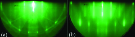
An n-type Si wafer with (111) orientation was used as the substrate to grow the ferromagnetic Fe3Si. After cleaning the substrates with an aqueous HF solution (HF : H2O 1 : 40), we conducted a heat treatment at 450 ∘C for 20 min in an MBE chamber with a base pressure of 2 10-9 Torr. A reflection high energy electron diffraction (RHEED) pattern of the flashed surface of the substrate displays symmetrical streaks, as shown in Fig. 1(a). This figure indicates atomic level flatness of the surface of the Si substrate. Prior to the growth of Fe3Si layers, the substrate temperature was reduced down to 130 ∘C. Using Knudsen cells, we co-evaporated Fe and Si with the growth rates of 2.12 and 1.20 nm/min, respectively. Figure 1(b) shows an RHEED pattern of the Fe3Si layer observed. The RHEED pattern clearly keeps symmetrical streaks, which implies good two-dimentional growth of the Fe3Si on Si(111). X-ray diffraction (XRD) measurements of the Fe3Si/Si(111) were also performed in and 2 configurations. In general, since the lattice mismatch between Fe3Si and Si is about 4 % for bulk samples, the diffraction peaks can be separated. For our samples, however, the intensity of the diffraction peak due to Fe3Si(111) was quite weaker than that due to Si(111), and then the Fe3Si(111) peak was overlapped by the foot of the strong Si(111) peak. As a result, we could separate hardly the diffraction peak due to the Fe3Si layer from that due to the Si substrate in measurements.ref1 Also, there was no peak due to other FexSiy compounds. From these results, we can judge that the Fe3Si layer is grown epitaxially on the Si(111) substrate with no secondary phase such as cubic-FeSi.
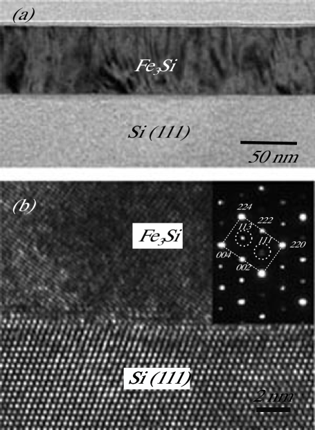
Figure 2 (a) shows a cross-sectional transmission electron microscopy (TEM) image of the Fe3Si/Si(111) structure. The interface between Fe3Si and Si(111) yields almost no marked roughness and no reaction layer. Also, selected area diffraction measurements revealed the absence of interfacial reaction phases such as cubic-FeSi (not shown here). A high-resolution TEM image near the Fe3Si/Si(111) interface is also shown in Fig. 2(b). The interface has a high-quality abruptness within the fluctuation of 2 3 monolayers. We also performed Rutherford backscattering spectroscopy (RBS) measurements of the Fe3Si/Si(111) and obtained the minimum yield () of 12 %. These results indicate that the Fe3Si/Si(111) maintains high crystallinity comparable to the Fe3Si/Ge(111) in our previous works.Sadoh ; Maeda Nanobeam electron diffraction patterns of the Fe3Si layers are also presented in the inset of Fig. 2(b). We can see evident superlattice diffractions, (111) and (113), caused by the presence of the ordered phase (white broken circles), in addition to fundamental reflections of the phases and superlattice reflections of the ordered phases. From these structural characterizations, the high-quality formation of the ordered single-crystal Fe3Si layers has been realized on the Si substrate at a quite low temperature of 130 ∘C.
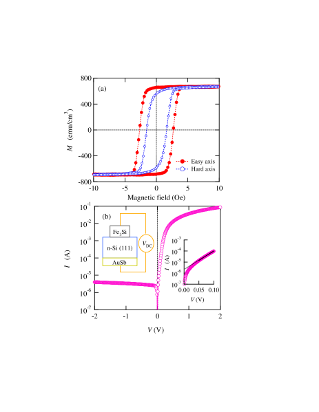
We also examine magnetic properties of the Fe3Si/Si(111). Field-dependent magnetization measured at room temperature is shown in Fig. 3(a), where the applied field directions are parallel to the magnetic easy and hard axes in the film plane. Evident hysteretic and magnetic anisotropic features can be seen, showing ferromagnetic nature. We find that the saturation magnetization is estimated to be 650 emu/cm3, i.e. 3.16 /f.u. From the depth profile measurements of Fe and Si atoms by energy dispersive x-ray spectroscopy and RBS, we determined the chemical composition of our sample as Fe2.84Si1.16. On the other hand, Lenz et al. have already reported that the saturation magnetization is 790 emu/cm3, i.e., 3.84 /f.u. for an epitaxial Fe3Si thin film with stoichiometric atomic composition.Lenz From these facts, since the Fe content of our sample is slightly lower than that of the stoichiometric samples, the lack of the magnetization can be explained by an influence of a small amount of the disordered phases.Ionescu ; Moss ; Ploog ; Nakane
Finally, to further evaluate the electrical properties of the Fe3Si/Si(111) interface, we fabricated Fe3Si/Si(111)/AuSb Schottky diodes, as shown in the left inset of Fig. 3(b), and measured the characteristics. Here, a resistivity of the used n-type Si(111) substrate is 1 5 cm (an impurity concentration of 1015 cm-3). We display absolute values of current as a function of bias voltage in the main panel of Fig. 3(b), where this behavior is reproduced for ten devices. A rectifying behavior indicating thermionic emission electron transport across a Schottky barrier can be observed, and the ratio of the current in forward bias to that in reverse bias is above 104. From fitting the data in the forward bias (0.05 V 0.1 V, see right inset),ref2 the Schottky barrier height () can roughly be estimated to be 0.62 eV, being in good agreement with obtained by its characteristic measurements. Note that the ideality factor becomes 1.08. These mean that the Fe3Si/Si(111) interface also demonstrates ideal electrical properties without interfacial defects.
In summary, we have realized epitaxial growth of ferromagnetic Fe3Si layers on Si (111) with keeping an abrupt interface using low-temperature molecular beam epitaxy at 130 ∘C. The grown Fe3Si layers have the ordered phase. We believe that development of this work can open up a road to operations of silicon-based spintronic devices with a spin injector and detector using the Fe3Si/Si interfaces.
The authors thank Prof. Y. Maeda of Kyoto University and Prof. K. Matsuyama and Prof. Y. Nozaki of Kyushu University for useful discussion and providing the opportunity to use a VSM. K.U. and Y.A. acknowledge support from JSPS Research Program for Young Scientists. This work was partly supported by a Grant-in-Aid for Scientific Research on Priority Area (No.18063018) from the Ministry of Education, Culture, Sports, Science, and Technology in Japan.
References
- (1) S. A. Wolf, D. D. Awschalom, R. A. Buhrman, J. M. Daughton, S. v. Molnár, M. L. Roukes, A. Y. Chtchelkanova, and D. M. Treger, Science 294, 1488 (2001).
- (2) S. Datta and B. Das, Appl. Phys. Lett. 56, 665 (1990).
- (3) S. Sugahara and M. Tanaka, Appl. Phys. Lett. 84, 2307 (2004).
- (4) K. C. Hall and M. E. Flatté, Appl. Phys. Lett. 88, 162503 (2006).
- (5) A. T. Hanbicki, B. T. Jonker, G. Itskos, G. Kioseoglou, and A. Petrou, Appl. Phys. Lett 80, 1240 (2002).
- (6) A. T. Hanbicki, O. M. J. van’t Erve, R. Magno, G. Kioseoglou, C. H. Li, B. T. Jonker, G. Itskos, R. Mallory, M. Yasar, and A. Petrou, Appl. Phys. Lett 82, 4092 (2003).
- (7) X. Lou, C. Adelmann, S. A. Crooker, E. S. Garlid, J. Zhang, S. M. Reddy, S. D. Flexner, C. J. Palmstrøm, and P. A. Crowell, Nature Physics 3, 197 (2007).
- (8) B. Min, K. Motohashi, C. Lodder, and R. Jansen, Nat. Mater. 5, 817 (2006); R. Jansen, Nat. Phys. 3, 521 (2007).
- (9) I. Appelbaum B. Huang, and D. J. Monsma, Nature 447, 295 (2007).
- (10) B. T. Jonker, G. Kioseoglou, A. T. Hanbicki, C. H. Li, and P. E. Thompson, Nature Physics 3, 542 (2007).
- (11) O. M. J. van’t Erve, A. T. Hanbicki, M. Holub, C. H. Li, C. Awo-Affouda, P. E. Thompson, and B. T. Jonker, Appl. Phys. Lett. 91, 212109 (2007).
- (12) K. Akeura, M. Tanaka, M. Ueki, and T. Nishinaga, Appl. Phys. Lett. 67, 3349 (2005).
- (13) T. Plake, T. Hesjedal, J. Mohanty, M. Kästner, L. Däweritz, and K. H. Ploog, Appl. Phys. Lett. 82, 2308 (2003).
- (14) A. Ionescu, C. A. F. Vaz, T. Trypiniotis, C. M. Gürtler, H. García-Miquel, J. A. C. Bland, M. E. Vickers, R. M. Dalgliesh, S. Langridge, Y. Bugoslavsky, Y. Miyoshi, L. F. Cohen, and K. R. A. Ziebeck, Phys. Rev. B 71, 094401 (2005).
- (15) Although the Si(222) peak is forbidden reflection theoretically, the small peak can be observed for actual Si substrates. Simultaneously, a quite small peak resulted from the Fe3Si(222) peak can also be detected near the Si(222) peak.
- (16) T. Sadoh, M. Kumano, R. Kizuka, K. Ueda, A. Kenjo, and M. Miyao, Appl. Phys. Lett. 89, 182511 (2006); K. Ueda, Y. Ando, M. Kumano, T. Sadoh, Y. Maeda, and M. Miyao, Appl. Sur. Sci. 254, 6215 (2008).
- (17) Y. Maeda, T. Jonishi, K. Narumi, Y. Ando, K. Ueda, M. Kumano, T. Sadoh, and M. Miyao, Appl. Phys. Lett. 91, 171910 (2007).
- (18) K. Lenz, E. Kosubek, K. Baberschke, H. Wende, J. Herfort, H. P. Schönherr, and K. H. Ploog, Phys. Rev. B 72, 144411 (2005).
- (19) J. Moss and P. J. Brown, J. Phys. F: Metal Phys. 2, 358 (1972).
- (20) J. Herfort, H. -P. Schönherr, K.-J. Friedland, and K. H. Ploog, J. Vac. Sci. Technol. B 22, 2073 (2004).
- (21) R. Nakane, M. Tanaka, and S. Sugahara, Appl. Phys. Lett. 89, 192503 (2006).
- (22) Following the thermionic emission model, we used next relationships, (qV/nkT 1), where . is the junction area of 7.6 10-3 cm2 and is the Richardson constant (110 A/cm2K2).