Magnetic Field Induced Instabilities in Localised Two-Dimensional Electron Systems
Abstract
We report density dependent instabilities in the localised regime of mesoscopic two-dimensional electron systems (2DES) with intermediate strength of background disorder. They are manifested by strong resistance oscillations induced by high perpendicular magnetic fields . While the amplitude of the oscillations is strongly enhanced with increasing , their position in density remains unaffected. The observation is accompanied by an unusual behaviour of the temperature dependence of resistance and activation energies. We suggest the interplay between a strongly interacting electron phase and the background disorder as a possible explanation.
The behaviour of electrons in presence of both disorder and interactions is one of the most fundamental questions in condensed matter physics Lee and Ramakrishnan (1985). While in strongly disordered and weakly interacting systems, single-particle localisation is expected Mott et al. (1975), the formation of a Wigner crystal (WC) has been predicted for the opposite regime of very strong interactions and absence of disorder Wigner (1934). Between those two regimes a variety of states has been proposed, ranging from a glassy phase Davies et al. (1982) to a pinned WC Chui and Tanatar (1995). A difficulty in the experimental investigation of interaction effects in disordered systems is that long-range disorder can cause charge inhomogeneities which lead to a percolation type transport, masking possible interaction effects Das Sarma et al. (2005).
Recently, a new approach for studying the influence of short-range disorder on strongly interacting 2DES has lead to the observation of a low-temperature collapse of electron localisation Baenninger et al. (2008a) and an interaction dominated hopping magnetoresistance Ghosh et al. (2004a); Baenninger et al. (2005); Baenninger et al. (2008b). These results are strong evidence of a breakdown of conventional single-particle transport generally observed in the strongly localised regime of 2DES Mott (1968); Efros and Shklovskii (1975). The experiments were carried out in mesoscopic electron systems in modulation doped GaAs/AlGaAs heterojunctions, extending only over a few microns in order to reduce the impact of long range charge inhomogeneities. The strength of disorder was controlled by varying the spacer width between 2DES and charged dopants which are the main source of disorder in these system.
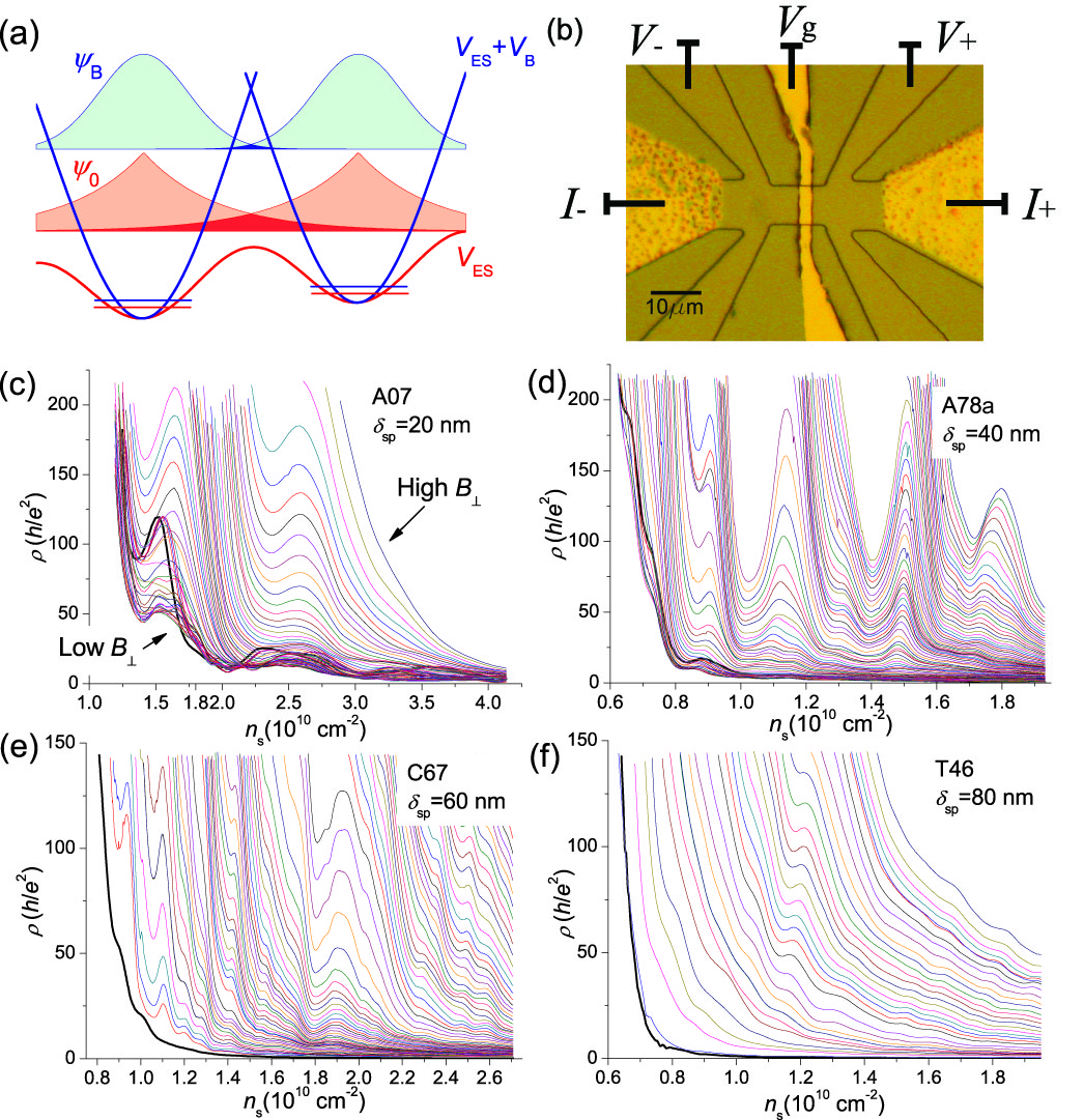
A magnetic field perpendicular to a 2DES introduces an effective parabolic confinement potential, which can localise electrons, reducing the wave function overlap between them [see schematic in Fig. 1 (a)], and quench their kinetic energy. This may effectively increase the strength of their Coulomb interaction. In this Letter, we investigate the impact of strong magnetic fields and its interplay with disorder on transport in mesoscopic 2DES. All devices were made from Si -doped heterojunctions with dimensions of the gated 2DES area ( width of the mesa, the length of the gate). A typical device is shown in Fig. 1 (b) and a list of devices is given in Table 1. Measurements were carried out in a 3He cryostat (base temperature 300 mK) with standard lock-in four probe setup with excitation frequency Hz and current =100 pA. The low current ensured linear response and minimal Joule heating. A slow cooldown from room temperature to 4 K over h gave best results. This could be related to enhanced correlations between charges in the dopant layer, which may reduce the long range disorder fluctuations Efros (1988). The gate voltage dependence of electron density was measured with a technique based on the reflection of edge states in the Quantum Hall regime Ghosh et al. (2004a).
| Device | ||||||
|---|---|---|---|---|---|---|
| nm | nm | cm-2 | cm-2 | cm2/Vs | ||
| A07 | 20 | 120 | 83 | 2.5 | 2.9 | |
| A78a | 40 | 290 | 82 | 2.5 | 2.1 | |
| A78b | 40 | 290 | 84 | 2.5 | 2.1 | |
| C67 | 60 | 290 | 83 | 0.7 | 1.0 | |
| T46 | 80 | 300 | 83 | 1.9 | 0.8 |
Figs. 1 (c)-(f) show the resistivity as a function of at stepwise increasing for four devices made from wafers with spacer widths =20, 40, 60 and 80 nm. While at zero magnetic field the resistance increases with decreasing in a relatively featureless way (thick black lines), when a magnetic field is applied, strong resistance oscillations appear with maximum amplitudes M. The amplitudes get larger with increasing , but the positions of peaks and troughs is virtually unaffected by changes of several Tesla. The positions were also highly stable over experimental runs of several weeks, including many gate voltage sweeps and dependence measurements up to K. The oscillations start developing at , which highlights the importance of the 2DES being localised. While peaks generally start appearing only at Landau level (LL) filling factor , no systematic connection to a certain filling factor can be observed and often changes by a factor of as a peak evolves at constant . This clearly rules out effects related to LLs, where peak positions would have to move with . The strength of the oscillations is similar for devices with nm [Fig. 1 (c)-(e)], but they practically disappear in a wafer of very low disorder with nm [Fig. 1 (f)]. Macroscopic devices () did not show any magnetically induced resistance oscillations (not shown).
The separation between two resistance peaks in terms of is usually cm-2, which corresponds to adding several hundred electrons to the active area of the 2DES for typical device dimensions. This makes it very unlikely that the observation is caused by single electron charging effects such as Coulomb blockade (CB) oscillations, which have previously been reported in mesoscopic 2DES Cobden et al. (1999). Equivalently, the spacing in terms of gate voltage mV e.g. for the device shown in Fig. 1 (d), would suggest a dot area with ( the separation between gate and 2DES) the capacitance per area for a parallel plate capacitor. This is a tiny area compared to the overall device area. In stark contrast to Fig. 1 (c)-(e) is the data shown in Fig. 4 (a). It shows the resistivity as a function of gate voltage for device A78b after an uncontrolled fast cooldown from room temperature to 4 K. Here, a non-monotonic dependence of is observed even at zero field (think black line) and with stepwise changes of , fast resistance oscillations appear and disappear, with positions of peaks and troughs changing in an apparently random manner. A very similar behaviour has also been reported in strongly disordered mesoscopic devices with nm Ghosh et al. (2004b). A “bad” cooldown, or small spacer may lead to larger disorder and, hence, to strong inhomogeneity of the electron distribution even on a mesoscopic length scale. This could lead to transport by tunnelling between electron “puddles”, where CB effects become important Raikh and Ruzin (2006); Tripathi and Kennett (2006). The data shown in Fig. 1 (c)-(e) shows a qualitatively different behaviour. We suggest that the smoother background disorder in a “good” cooldown leads a homogeneous electron distribution on the scale of the device size. Indeed, in several controlled slow cooldowns, device A78b showed a very similar behaviour to A78a [Fig. 1 (d)]. Additional evidence for a qualitatively different phenomenon comes from the fact that a line shape expected for CB could be fitted satisfactorily to the oscillations observed in the “bad” cooldown as well as in the devices with nm Ghosh et al. (2004b). However, for the oscillations shown in Fig. 1 (c)-(e), the agreement of the fit was poor.
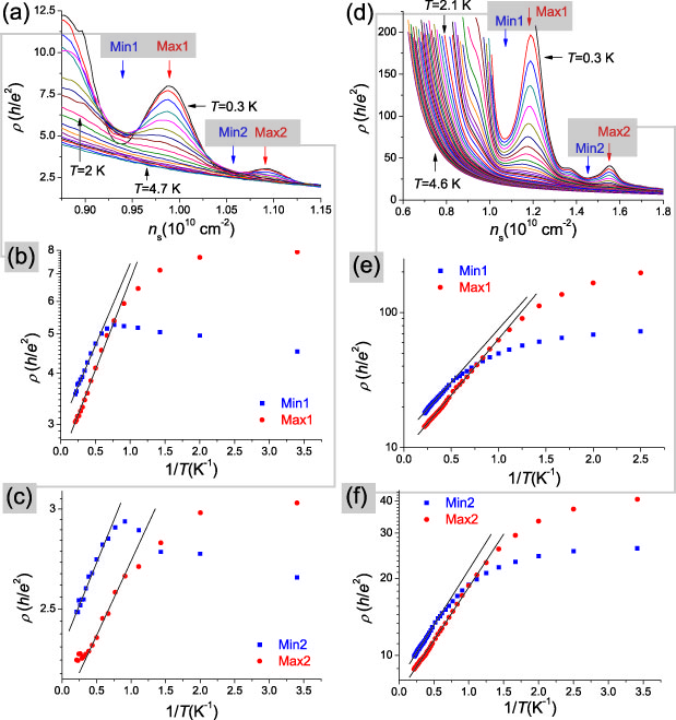
The dependence of in the regime of strong oscillations for two devices at =0.5 and 2 T is given in Fig. 2. Panels (a) and (d) show the oscillations at stepwise changing K. The oscillations are damped strongly with increasing and have virtually disappeared by K. Panels (b), (c), (e) and (f) show vs. at several values of , each panel comparing the dependence of a resistance trough to the next peak with increasing . Generally, the dependence in our devices at low enough electron densities can be divided into two regimes: At high , a strongly insulating (activated) behaviour is always observed, but at low enough temperatures a qualitatively different behaviour occurs with becoming weakly dependent (saturated) or even decreasing with decreasing temperature (metallic) Baenninger et al. (2008a); Ghosh et al. (2004a); Baenninger et al. (2005); Baenninger et al. (2008b). This finding is confirmed by the results in Fig. 2. Let us first focus on the low part. The 60 nm spacer device at relatively small field T shows a striking difference between peaks and troughs [Fig. 2 (a)-(c)]. At the positions of peaks, the dependence weakens at lowest temperatures and deviates from the high activated behaviour. The troughs also show such a deviation, however, here, the dependence is non-monotonic and starts dropping as is lowered further. This observation clearly suggests a connection between the origin of the oscillations and the previously reported metallic behaviour in our devices Baenninger et al. (2008a). At a higher field T for the 40 nm spacer device a clear difference between peaks and troughs is still observed [Fig. 2 (d)-(f)]. However, the metallic behaviour is replaced with a strong saturation. This is again in agreement with previous observation that the metallic phase was suppressed at T Baenninger et al. (2008a). The saturation is much stronger in case of troughs than peaks and the deviation from exponential behaviour sets in at higher .
The activated part of the dependence provides important information about the energy scale that dominates transport in this regime, via the activation energy which can be extracted from fits of the form (solid lines in the lower panels of Fig. 2), with the Boltzmann constant. In Fig. 3 is plotted as a function of for various , combined with the resistance oscillation of the same device.
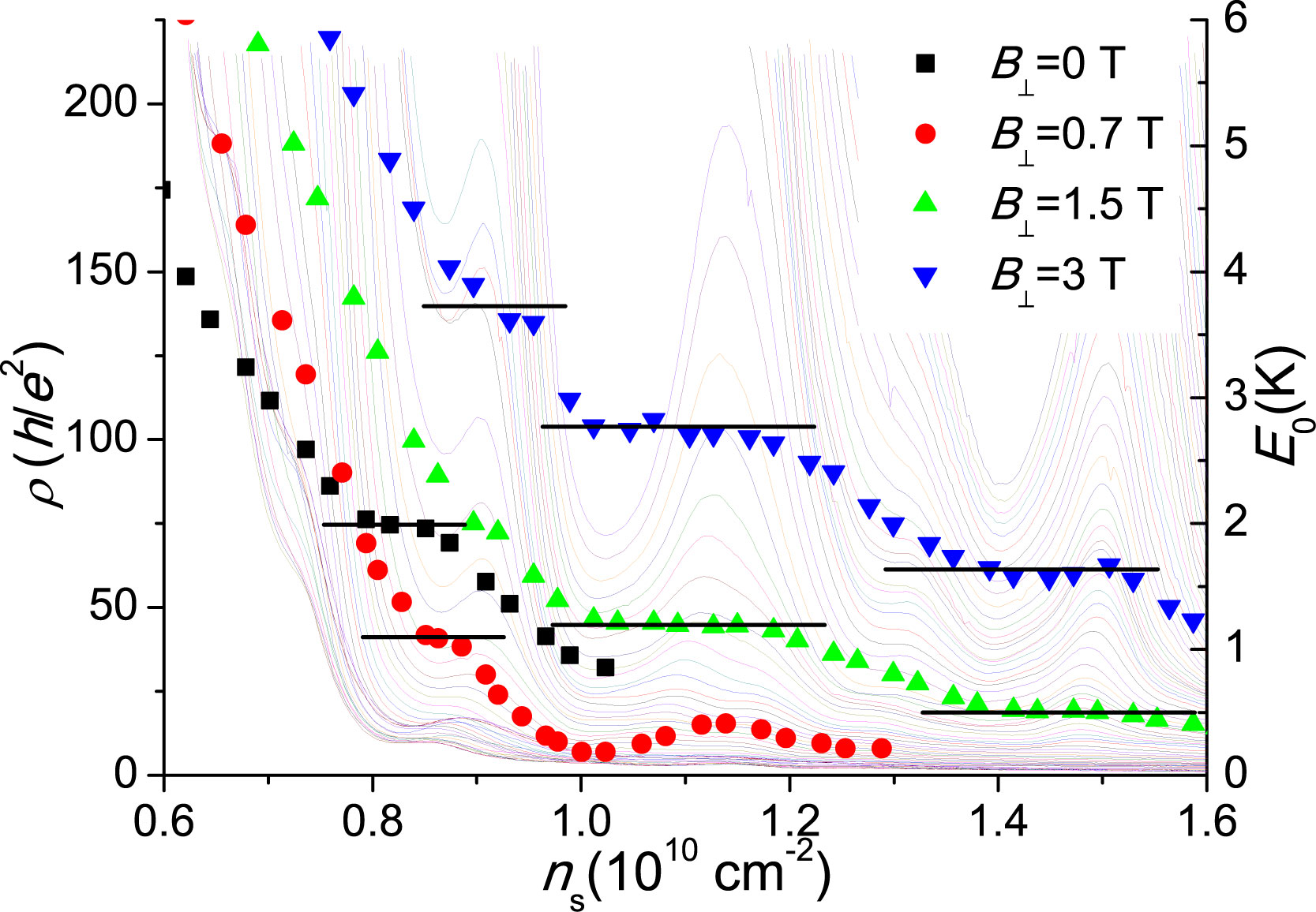
It exhibits a striking behaviour: An overall decrease of with increasing is observed, but clear plateaux are formed between troughs and next following peaks. The plateaux (highlighted by horizontal lines) are strongest at higher fields and 3 T, but are observed even at , where resistance oscillations are absent. This behaviour is particularly remarkable when noticing that the exponential fits are done in the high regime where the oscillations are suppressed in simple resistance measurements. If the activated behaviour is caused by excitation of charge carriers to a mobility edge (e.g. activation across a potential barrier), the dependence of provides information about the compressibility of the system, with a flat behaviour evidence of a pinning of the Fermi energy by a highly compressible phase. In this view, the observed behaviour would suggest a repeated transition between compressible and incompressible states. Note that the monotonic dependence of also gives further evidence against a CB effect, where an oscillatory dependence of is expected, with disappearing at resonance (resistance minima).
The large separation in terms of between the peaks suggests a phenomenon involving many electrons as the origin of the observation, rather than single charging events. We have previously presented evidence of formation of a disorder stabilised electron solid (ES) in our systems, where transport occurs by tunnelling of defects. This was mainly supported by the observation that the average hopping distance of the charge carriers was approximately equal to the average electron-electron separation Ghosh et al. (2004a); Baenninger et al. (2005). If a pinned ES was formed in our relatively disordered 2DES, one would expect a complex interplay between the ES (or, indeed, any strongly correlated electron phase) and the background disorder potential as the electron density is varied. This could lead to a ”locking” of the ES over a certain density range, where most of the electrons remain in their positions while additional electrons are added to interstitial positions. At some point a large scale rearrangement/relaxation of the solid may occur with a strong impact on transport properties. Such repeated rearrangements, possibly accompanied by changes in the degree of ordering in the solid, could explain the the resistance oscillations, as well as the behaviour of (plateaux when the solid is ”locked” with a pinning of due to a large density of defect states). The peculiar dependence could then arise from a transition from activated transport (high ) to a near-resonant tunnelling of defects (low ) with metallic behaviour caused by defect delocalisation if disorder is not too strong Baenninger et al. (2008a). The magnetic field may be required to induce or stabilise the ES by reducing the wave function overlap between electrons, an effect that has long been proposed Lozovik and Yudson (1975). Another possible mechanism based on stripe formation in an electron lattice has been proposed to cause resistance oscillations Slutskin et al. (2000).
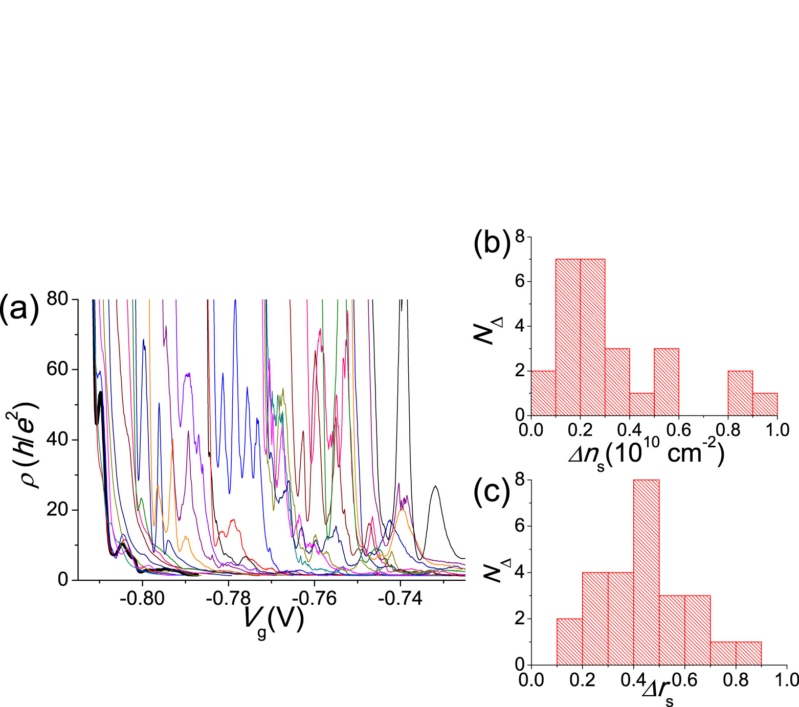
Finally, we will discuss another unexpected observation, namely that the positions of the peaks may not be entirely random. It was found that most devices showed particularly strong peaks in the proximity of 1.2 and 1.8 cm-2. In view of previous results highlighting the importance of the average electron-electron separation Ghosh et al. (2004a); Baenninger et al. (2005) we have analysed the peak positions in terms of the interaction parameter ( the effective Bohr radius), which gives a dimensionless expression for . One immediately notices that and cm-2, correspond to the integer values and 4. Furthermore, we found the separation between peaks to be approximately 0.5 in terms of . This is confirmed by the histograms of the peak separation shown in Figs. 4 (b), and (c), where we have anylised 10 devices from five different wafers (-doped with , 40, 60 and 80 nm and bulk doped with nm with ). While (b) exhibits a peak around cm-2 but otherwise apparently random distribution (c) shows a clear, if broad maximum around . A similar analysis in terms of absolute value of is difficult because of the relatively small number of devices and the experimental error in . Nevertheless, our observation gives some indication of a distinction of integer and half integer values of , which is further supported by previous experiments in the localised regime of 2DES of similar dimensions to the ones used here Pepper (1979); Ghosh et al. (2004b). Although a definite statement in this matter will require more work, a possible universality in such a fundamental quantity as should not go unmentioned due to its far reaching implications. It would suggest fundamental density dependent instabilities of currently unknown origin, which could not be directly related to details of background disorder, although disorder could still play a role in enhancing electron-electron interactions in combination with the magnetic field.
We thank EPSRC and the UK-India Education and Research Initiative (UKIERI) for financial support. MB thanks the COLLECT network and the Sunburst and Cambridge Overseas Trusts.
References
- Lee and Ramakrishnan (1985) P. A. Lee and T. V. Ramakrishnan, Rev. Mod. Phys. 57, 287 (1985).
- Mott et al. (1975) N. Mott et al., Proc. R. Soc. Lond. A. 345, 169 (1975).
- Wigner (1934) E. Wigner, Phys. Rev. 46, 1002 (1934).
- Davies et al. (1982) J. H. Davies, P. A. Lee, and T. M. Rice, Phys. Rev. Lett. 49, 758 (1982).
- Chui and Tanatar (1995) S. T. Chui and B. Tanatar, Phys. Rev. Lett. 74, 458 (1995).
- Das Sarma et al. (2005) S. Das Sarma et al., Phys. Rev. Lett. 94, 136401 (2005).
- Baenninger et al. (2008a) M. Baenninger et al., Phys. Rev. Lett. 100, 16805 (2008a).
- Ghosh et al. (2004a) A. Ghosh et al., Phys. Rev. B 70, 233309 (2004a).
- Baenninger et al. (2005) M. Baenninger et al., Phys. Rev. B 72, 241311(R) (2005).
- Baenninger et al. (2008b) M. Baenninger et al., Physica E: Low-dim. Syst. Nanostruct. 40, 1347 (2008b).
- Mott (1968) N. F. Mott, J. Non-cryst. Solids 1, 1 (1968).
- Efros and Shklovskii (1975) A. L. Efros and B. I. Shklovskii, J. Phys. C: Solid State Phys. 8, L49 (1975).
- Efros (1988) A. L. Efros, Solid State Comm. 65, 1281 (1988).
- Cobden et al. (1999) D. H. Cobden, C. H. W. Barnes, and C. J. B. Ford, Phys. Rev. Lett. 82, 4695 (1999).
- Raikh and Ruzin (2006) M. E. Raikh and I. M. Ruzin, in Mesoscopic Phenomena in Solids, edited by B. L. Altshuler, P. A. Lee, and R. A. Webb (North-Holland, Amsterdam, 1991), p. 301.
- Tripathi and Kennett (2006) V. Tripathi and M. P. Kennett, Phys. Rev. B 74, 195334 (2006); Phys. Rev. B 76, 115321 (2007).
- Ghosh et al. (2004b) A. Ghosh et al., J. Phys.: Condens. Matter 16, 3623 (2004b).
- Lozovik and Yudson (1975) Y. E. Lozovik and V. I. Yudson, JETP Lett. 22, 11 (1975).
- Slutskin et al. (2000) A. A. Slutskin, V. V. Slavin, and H. A. Kovtun, Phys. Rev. B 61, 14184 (2000).
- Pepper (1979) M. Pepper, J. Phys. C: Solid State Phys. 12, L617 (1979).