Infrared spectroscopy of electronic bands in bilayer graphene
Abstract
We present infrared spectra (0.1-1 eV) of electrostatically gated bilayer graphene as a function of doping and compare it with tight binding calculations. All major spectral features corresponding to the expected interband transitions are identified in the spectra: a strong peak due to transitions between parallel split-off bands and two onset-like features due to transitions between valence and conduction bands. A strong gate voltage dependence of these structures and a significant electron-hole asymmetry is observed that we use to extract several band parameters. Surprisingly, the structures related to the gate-induced bandgap are much less pronounced in the experiment than predicted by the tight binding model.
Since the first successful attempt to isolate graphene NovoselovScience04 , this two-dimensional material remains in the focus of active research motivated by a unique combination of electronic properties and a promising potential for applications GeimNovoselovNatMat07 . Its infrared response, like many other transport and spectral properties, is notably distinct from the one of conventional metals and semiconductors. For example, the optical conductance of monolayer graphene, which describes the photon absorption by a continuum of electronic transitions between the hole and electron conical bands, remains constant in a broad range of photon energies and equal to AndoJPSJ02 ; NairScience08 ; LiNP08 . Quite remarkably, the optical transmittance of single carbon layer in this range depends solely on the fine structure constant KuzmenkoPRL08 ; NairScience08 . In bilayer graphene, where the interlayer electron hopping results in two extra electron and hole bands separated from the main bands by about 0.4 eV, one expects to see a set of intense and strongly doping dependent infrared structures NilssonPRL06 ; AbergelFalkoPRB07 ; NicolCarbottePRB08 sensitive to various band details and quasiparticle scattering rates. This makes infrared spectroscopy a powerful probe of the low-energy electronic dispersion in graphene, especially in combination with a possibility to electrostatically control the doping level JiangPRL07 ; LiNP08 ; WangScience08 . Here we present infrared spectra of bilayer graphene crystals in a broad doping range, which allows us to observe new features, in particular a significant electron-hole asymmetry. By comparing data with the tight binding Slonczewski-Weiss-McClure (SWMcC) model SWMcC we identify interband transitions and determine some band parameters.
Bilayer graphene is considered to be particularly important for electronics applications by virtue of a bandgap that opens when there is difference between the electrostatic potential of the two layers McCannFalkoPRL06 ; GuineaPRB06 ; McCannPRB06 ; OhtaScience06 ; CastroPRL07 ; OostingaNatMat08 . Angle-resolved photoemission (ARPES) measurements indicate such a gap in potassium doped bilayer graphene epitaxially grown on SiC OhtaScience06 . Although transport experiments CastroPRL07 ; OostingaNatMat08 demonstrate that a bandgap also opens in gate-tunable bilayer graphene flakes, no spectroscopic information about the size of the gate-induced gap is currently available. The analysis of infrared data allows us to get further insight into this issue.
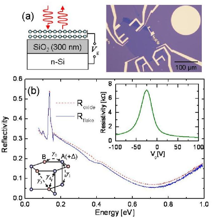
The sample used in this study is a large (100 m) bilayer graphene flake (Graphene Industries Ltd.) on top of an n-doped Si substrate covered with a 300 nm layer of SiO2 (Fig.1(a)). A field-effect device configuration allowed us to simultaneously measure the DC resistivity and infrared reflectance as a function of the applied gate voltage . Optical spectra in the photon energy range 0.1-1 eV were collected at 10 K with an infrared microscope (Bruker Hyperion 2000) focussing the beam on a spot of about 30 microns in diameter. The absolute reflectance of graphene, , and of the bare substrate, , (Fig.1(b)) were obtained by using a circle of gold deposited close to the sample as a reference mirror. The bare substrate spectrum features intense optical phonon modes in SiO2 below 0.15 eV and a dip at 0.7 eV due to the Fabry-Perot effect in the SiO2 layer. The change of the absolute reflectivity introduced by graphene is small but reproducibly measurable as we checked on a second sample. By taking difference spectra, we largely cancel spurious optical effects such as a weak 0.4 eV absorption band due to some frozen water. The resistivity maximum that corresponds to zero doping (Fig.1(b), inset) is found to be at = -25 V instead of 0 V, which we attribute to a charging effect by contaminant molecules.
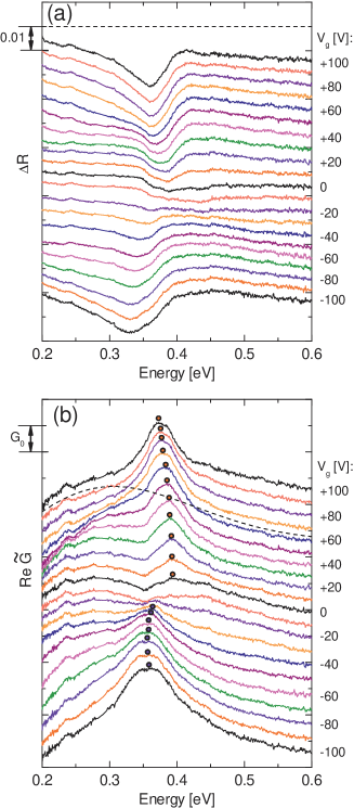
The curves of between 0.2 and 0.6 eV are shown in Fig.2(a) as a function of the gate voltage from -100 V to +100 V. The spectra in this region are very sensitive to the gate voltage and show a significant asymmetry between the electron () and the hole () doping. Since it is more convenient to discuss the data in terms of the real part of the optical conductance , we extracted this quantity by a Kramers-Kronig (KK) constrained inversion KuzmenkoRSI05 of the raw reflectivity data. Due to a sensitivity of the inversion procedure to the systematic uncertainty ( 0.005) of and to the data extrapolations beyond the experimental spectral range (we used graphite optical data KuzmenkoPRL08 as the most reasonable extrapolation) the inverted function is likely to contain a spectrally smooth background as compared to . Although this background does not allow us to determine accurately the absolute conductance, it affects the positions of spectral structures and their doping dependence to a much lesser extent.
The spectra of (Fig.2(b)) reveal a prominent peak centered between 0.35 and 0.4 eV, whose intensity increases with the absolute value of the gate voltage and vanishes as approaches . Based on previous theoretical works NilssonPRL06 ; AbergelFalkoPRB07 ; NicolCarbottePRB08 as well as on the calculations described below we assign this peak to a transition between the hole bands 1 and 2 (marked as C in Fig.3(e)) for and to the one between the electron bands 3 and 4 (marked as B) for . The doping induced shift of the Fermi level away from the Dirac point expands the momentum space, where this transition is allowed by the electronic occupation of the initial and the final states, and therefore increases the infrared intensity of the peak.
The energy of this peak is given by the band separation and is close to the interlayer vertical hopping parameter (shown in the inset of Fig.1(b)). In the case of precisely symmetric electron and hole bands, one would expect the same peak position for the positive and negative gate voltages. However, the data reveal a clear asymmetry: at positive voltages the maximum (marked with red circles in Fig.2(b)) is higher in energy and shows a much stronger dependence on than at negative voltages (blue circles). As was pointed out in Ref.LiCM08, , the energy of the peak on the electron and hole side taken close to the charge neutral point ( = -25 V in our case) is equal to and respectively, where the parameter is the potential difference between carbon sites A and B. These values in our case are 0.393 0.005 eV and 0.363 0.005, which yields eV and eV. The value of is very close to 0.377 eV found in graphite ChungReview . However, it is somewhat smaller than 0.404 eV reported in Ref.LiCM08, for bilayer graphene flake. This suggests that the interlayer distance, to which is the most sensitive, may change from sample to sample. As far as is concerned, there is much less agreement on the value of this parameter in graphite in the literature. While the magnetoreflection and de Haas - van Alphen measurements suggest that is -0.008 eV (see Ref.ChungReview, and references therein), infrared data GuizzettiPRL73 ; KuzmenkoPRL08 give a value of +0.04 eV. Our value agrees in sign with the infrared-based estimate in graphite, but is about 2-3 times smaller. This difference can be understood using electrostatics arguments. In Bernal stacked graphite, each carbon layer is symmetrically surrounded by two other layers, in contrast to bilayer graphene. Therefore one may expect the difference between the (screened) Coulomb potential on sites A and B induced by charges on other layers to be larger in graphite.
In order to get further insight, we compare the experimental data with calculations based on the tight binding SWMcC model that proved to be very successful in graphiteSWMcC ; PartoensPRB06 ; KuzmenkoPRL08 . The hopping terms considered are shown in the inset of Fig.1(b). The values of all band parameters except and , which were determined above were taken from Ref. PartoensPRB06, : = 3.12 eV, = 0.378 eV , = 0.29 eV, = 0.12 eV and = 0.015 eV. Note that they agree well with the values determined in Ref.MalardPRB07 using Raman spectroscopy. The doped charge and the Fermi energy can be directly determined for any given gate voltage using the known capacitance of the SiO2 layer CastroPRL07 . The Kubo formula was used to calculate that was eventually Gaussian-broadened by 0.02 eV, in order to match the observed line widths. The reflectivity spectra were computed based on Fresnel equations using the known optical properties of the SiO2/Si substrate. We begin with a calculation which assumes that the only effect of applying gate voltage is to shift the chemical potential and does not include the gate-induced bandgap.
In panels (a) and (c) of Fig.3, the color plots of experimental and calculated spectra of are represented. One can notice a quite good correspondence between the energy and the gate voltage dependence of the strong spectral features. Having found that such an agreement is present in the raw reflectivity data, we proceed with a detailed experiment-theory comparison in terms of the optical conductance (Fig.3(b) and (d)). In view of the mentioned possibility that the extracted conductance curves contain a spectrally featureless background, here we subtract from all spectra the same, i.e. gate-voltage independent, smooth curve shown as a dashed line in Fig.2(b). This curve is chosen in such a way that the corrected coincides with the theoretical values in the regions around 0.2 eV and 0.6 eV, where no sharp structures are expected.
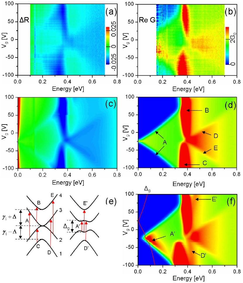
The assignment of the optical conductance structures to interband transitions is given in Fig.3(d). Apart from the discussed strong peak structures B and C there is an onset-like structure A which corresponds to a transition between the low-energy bands 2 and 3, which has the same origin as the onset-like structure observed in monolayer graphene LiNP08 . The onset frequency is twice the Fermi level with respect to the Dirac energy, which is in bilayer graphene proportional to with a coefficient determined by . In the measured spectra (Fig.3(b)) we observe such a structure showing the same (within the experimental uncertainty) dependence on the gate voltage. This confirms that is close the value used in the calculation (3.12 eV). This observation is in accordance with a recent measurement of Li et al. LiCM08 . Interestingly, there is a second onset-like structure, with the onset energy showing a similar V-shape dependence on the gate voltage but shifted with respect to the structure A by about . The structure is due to the onset of transition D () for the electron doping and transition E () for the hole doping. There is a significant enhancement of close to the ’vertex’ point , where the two onsets are close to each other NilssonPRL06 ; AbergelFalkoPRB07 . One can clearly see a similar structure on the experimental graph. Thus the tight binding model reproduces most of the features of experimental spectra.
Now we address the issue of the gate-induce bandgap between the low-energy electron and hole bands McCannFalkoPRL06 ; GuineaPRB06 ; McCannPRB06 . Its manifestation in the infrared spectra was first calculated (assuming that , and = 0) in Ref.NicolCarbottePRB08 . In Fig.3(f) we show the result of a calculation where we keep the all aforementioned band parameters and add a gate-dependent difference in electrostatic potential between the two planes. We use a curve from Ref.CastroPRL07, , shown as a red line in Fig.3(f), where the charge screening effects were treated self-consistently. We assume, as it was also done in Ref.CastroPRL07, , that contaminant molecules shifting the charge neutrality point away from act as an effective top gate electrode. In this case the bandgap vanishes not at but at . At the highest gate voltages of our experiment the gap value is expected to be of the order of 0.1 eV.
According to the calculation, the opening of the bandgap indeed brings some extra features to the spectra. All of them are due to the flattening of bands 2 and 3, as shown in Fig.3(e), which results in a strong increase of the density of states of these bands. The first feature (marked A’) is an enhancement of the optical intensity of the transition . Although this enhancement largely shows up at photon energies below the experimentally accessible region, its tail spreads up to about 0.2 eV. The second feature is the appearance of high-frequency satellites (marked E’ and D’) to the peak-like structures B and C. These satellites correspond from transitions and respectively. The energy separation between the central frequencies of peaks B and E’ as well as between C and D’ is close to the energy of the bandgap and could be therefore read directly from the conductance curves. Note that the interband structures A’, E’ and D’ involve the same band pairs as the structures A, E and D respectively. However the former ones are exclusively due to transitions within a very small momentum region around the Dirac point.
We notice that experimental spectra (Fig.3(b)) show an enhancement of conductance similar to the high-frequency tail of the structure A’. However the satellite structure E’ and D’ are not obviously present in the data. Thus the tight binding model that is quite successful in describing the main infrared features, is only in partial agreement with the data as far as the bandgap related features are concerned. This fact is perhaps the largest surprise of our study. We can only speculate about the possible reasons. First of all, the satellite features might be smeared out by doping inhomogeneity, due to the flake corrugation, contaminant molecules or other factors. However, the calculation already takes a large broadening (about 0.02 eV) into account. A second possibility is that the actual bandgap is smaller than the prediction of a simple model that does not take into account interaction effects, so that the satellites E’ and D’ cannot be easily separated from the main peaks. A third possibility is that the gap can be partially filled with impurity states NilssonPRL07 . Future experimental and theoretical developments are required to resolve this intriguing issue.
This work was supported by the Swiss National Science Foundation through the National Center of Competence in Research ”Materials with Novel Electronic Properties-MaNEP”. We are grateful to A. Morpurgo, L. Benfatto, E. Cappelluti and M. Fogler for helpful discussions.
References
- (1) K.S. Novoselov, A.K. Geim, S.V. Morozov, D. Jiang, Y. Zhang, S.V. Dubonos, I.V. Grigorieva, A.A. Firsov, Science 306, 666 (2004).
- (2) A. K. Geim, K. S. Novoselov, Nature Mater. 6, 183 (2007).
- (3) T. Ando, Y. Zheng, H. Suzuura, J. Phys. Soc. Japan 71, 1318 (2002).
- (4) R.R. Nair, P. Blake, A.N. Grigorenko, K.S. Novoselov, T.J. Booth, T. Stauber, N.M.R. Peres, A.K. Geim, Science 320, 1308 (2008).
- (5) Z.Q. Li, E.A. Henriksen, Z. Jiang, Z. Hao, M.C. Martin, P. Kim, H.L. Stormer, and D.N. Basov , Nature Physics 4, 532 (2008) .
- (6) A. B. Kuzmenko, E. van Heumen, F. Carbone, D. van der Marel, Phys. Rev. Lett. 100, 117401 (2008).
- (7) J. Nilsson, A. H. Castro Neto, F. Guinea, and N. M. R. Peres, Phys. Rev. Lett. 97, 266801 (2006).
- (8) D. S. L. Abergel and V. I. Fal’ko, Phys. Rev. B 75, 155430 (2007).
- (9) E. J. Nicol and J. P. Carbotte, Phys. Rev. B 77, 155409, (2008).
- (10) Z. Jiang, E.A. Henriksen, L.C. Tung, Y.-J. Wang, M.E. Schwartz, M.Y. Han, P. Kim, H.L. Stormer, Phys. Rev. Lett. 98, 197403 (2007).
- (11) F. Wang, Y. Zhang, C. Tian, C. Girit, A. Zettl, M. Crommie, Y. R. Shen, Science 320, 206 (2008).
- (12) J.W. McClure, Phys. Rev. 108, 612 (1957); J.C. Slonzcewski and P.R. Weiss, Phys. Rev. 109, 272 (1958).
- (13) D. McCann, V.I. Falko, Phys. Rev. Lett. 96, 086805 (2006).
- (14) F. Guinea, A.H. Castro Neto and N.M.R. Peres, Phys. Rev. B 73, 245426 (2006).
- (15) E. McCann, Phys. Rev. B 74, 161403(R) (2006).
- (16) T. Ohta, A. Bostwick, T. Seyller. K. Horn, E. Rotenberg, Science 313, 951 (2006).
- (17) E. V. Castro et al., Phys. Rev. Lett. 99, 216802 (2007).
- (18) J. B. Oostinga, H.B. Heersche, X. Liu, A.F. Morpurgo, L.M.K. Vandersypen, Nature Mater. 7, 151 (2008).
- (19) A.B. Kuzmenko, Rev. Sci. Instrum. 76, 083108 (2005).
- (20) D. D. L. Chung, J. Mat. Science 37, 1 (2002).
- (21) G. Guizzetti, L. Nosenzo, E. Reguzzoni, and G. Samoggia, Phys. Rev. Lett. 31, 154 (1973).
- (22) Z. Li et al., cond-mat/0807.3776; L. M. Zhang et al., cond-mat/0809.1898.
- (23) B. Partoens and F.M. Peeters, Phys. Rev. B 74, 075404 (2006).
- (24) L.M. Malard, J. Nilsson, D.C. Elias, J.C. Brant, F. Plentz, E.S. Alves, A. H. Castro Neto, and M. A. Pimenta, Phys. Rev. B 76, 201401(R) (2007).
- (25) J. Nilsson and A.H. Castro Neto, Phys. Rev. Lett. 98, 126801 (2007).