Relevant energy scale in hybrid mesoscopic Josephson junctions
Abstract
Transport properties of high quality Nb/semiconductor/Nb long Josephson junctions based on metamorphic In0.75Ga0.25As epitaxial layers are reported. Different junction geometries and fabrication procedures are presented that allow a systematic comparison with quasiclassical theory predictions. The impact of junction transparency is highlighted and a procedure capable of yielding a high junction quality factor is identified.
pacs:
Valid PACS appear hereSuperconductor/semiconductor hybrid devices are of much interest not only for their potential for electronic-device implementation but also as model systems for the investigation of the phenomena regulating the conversion of supercurrent into normal current at the interface through Andreev reflection BTK . By taking advantage of the increasing availability of ultra pure nanoscale semiconductors, major advances on the understanding of the microscopic nature of Josephson coupling and the interplay between superconductivity and mesoscopic effects can be expected IcQuant ; IcKondoCNT ; IcCB . Recent examples are the demonstration of the control of Josephson current in diffusive InAs nanowires coupled to superconducting leads (J-dot) IcCB and the study of the interplay between quantum interference effects and superconducting correlation doh07 ; giazotto . Arguably, the main limiting factor for the exploitation of hybrid systems in practical devices is the low value of the junction quality factor (i.e. critical current value times normal resistance). In fact, with few exceptions note ; crestin , this is the parameter normally referred to in the literature Heida98 ; schapers98 ; kroemer . It is crucial to have the largest possible value of , since, for instance, the maximum voltage amplification that can be obtained from a Josephson-Fet Clark1980 or a J-Dot IcCB is proportional to . The values of found in experimental works, however, are far from those predicted by theory. This rises several issues about the actual nature of these junctions and motivated transport analysis such as the one reported here.
The reduction of for semi/super Josephson junctions was already discussed in terms of reduced dimensionality of the normal conductor Kresin86 , low transparency of semi/super interfaces Kuprianov88 , diffusive interface Heida98 , and decoherence effects schapers98 . In a recent work Hammer et al. studied superconductor-normal-superconductor (SNS) junctions with non-ideal S/N interfaces Hammer2007 . These authors predicted that the Thouless energy () is replaced by the proximity induced gap in the normal region as the relevant energy scale governing, for instance, the temperature dependence of the critical current (In a diffusive system with ideal transparent interfaces ).
The objective of our work is two-fold: i) to investigate experimentally the theoretical predictions on the impact of the actual transparency of SN interfaces on SNS systems and ii) to identify a processing strategy capable of yielding high quality junctions. We shall examine various junctions characterized by different transparencies and N regions of various length and compare experimental Ic vs T curves for different fabrication processes. From these curves, thanks to the knowledge of the parameters of N material , we shall be able to analyze our data in the frame of ref. Hammer2007, and identify the process yielding the maximum interface transparency. In particular, we report a semiconductor/superconductor interface configuration for which is close to mV for a junction length of nm, among the best results ever obtained for such hybrid devices.
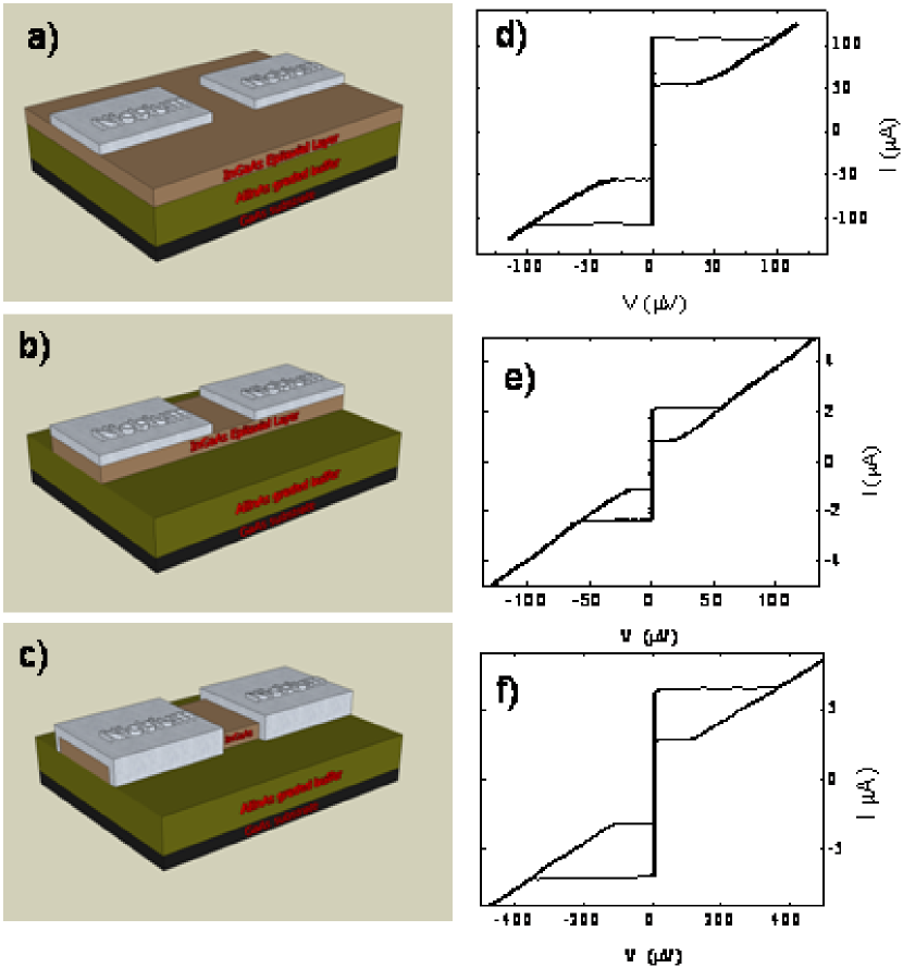
In the hybrid devices of interest here, the normal conductor is an epitaxial layer of In0.75Ga0.25As bulk-doped with silicon. Thickness is in the 50nm-200nm range. Structures were grown by molecular beam epitaxy (MBE) on a GaAs -oriented substrate tasc . A sequence of InxAl1-xAs layers of increasing In content was first deposited in order to ensure lattice matching with the upstanding layer of In0.75Ga0.25As. Before Nb deposition we performed a two-step surface cleaning of the semiconductor consisting of a first wet removal of the native oxide using diluted (1/50) HF solution and a subsequent vacuum RF discharge cleaning at very low power in Argon. Nb was then sputtered during the same vacuum cycle and electrodes were defined by lift-off. All Nb films were 85nm thick. We shall call the device obtained with this process type “A” (Fig. 1-a). Type “A” (Junctions J1 and J2 reported in Table 1) were fabricated on a 200nm thick epilayer with charge density m-3 and mobility 0.69m at K in the dark. A second type of device was fabricated on 50nm thick epitaxial layers with charge density m-3 and mobility 0.52m. We defined the semiconductor geometry (junction width) by employing a negative e-beam resist as a mask and subsequent wet chemical etching in H2SO4/ H2O2/H2O solution. This type of device will be labeled“B” and is showed in Fig. 1-b. A third type (“C”, shown in Fig. 1-c) of junction was obtained realizing the semiconductor mesa before Nb deposition. A Ti mask is first defined on the substrate by e-beam lithography, Ti thermal evaporation and lift-off. In0.75Ga0.25As structures are then defined by reactive ion etching. The last step is Nb deposition using the same technique described for type “A”. For type “C” we employed the same epitaxial layers of type “B”. For all samples the transition temperature of Nb leads is K, from which, using , we calculate mV.
Measurements were performed as a function of temperature down to mK in an 3He cryostat. Current and voltage leads were filtered by RC filters at room temperature. A second filtering stage consisted of RC + copper-powder filters thermally anchored at 1.5K-1.9K. The last copper-powder filter stage was at 250mK, thermally anchored to the 3He pot. The shielding from magnetic field was ensured by a combination of nested cryoperm, Pb and Nb foils all of them placed in the measurement dewar and immersed in liquid 4He.
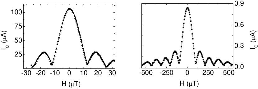
In all junctions, with normal conductor lengths typically ranging between 250nm and 1.1m, we found a measurable supercurrent, see Fig.1 panels d-f. For type A structures, we measured the critical current in different junctions made on the same chip (the same transparency was assumed in this case). These junctions had different values of electrode gap (1.1m to 250nm) and consequently of barrier length. Data are consistent with an exponential decrease of Ic vs. L like in metallic SNS dubos . The Fraunhofer-like patterns shown in Fig.2 confirm the Josephson nature of the zero voltage current. The period measured for junctions of different widths and lengths is consistent with theoretical expectations, which take into account flux focusing effects ff . The critical current was evaluated using a criterion, while was determined from a linear fit of I-V curves at .
For short () and tunnel junctions the only relevant energy scale is the gap of the superconductor and at low temperatures saturates at the value . In the ideal case of SN interfaces with zero resistance and very long SNS junctions (), determines both the value at which saturates at and the characteristic temperature of its exponential decrease. In this limit is not related to but only to through the expression , where . While the ratio decreases, gets smaller. The complete dependence on is reported in Ref. dubos, . The proportionality between and for very long junctions was experimentally demonstrated in the case of metallic SNS with transparent SN barriers dubos . For increasing SN interface resistance Hammer et all. Hammer2007 showed that vs curves change their concavity from downward to upward and the energy scale of their temperature decay is determined by an effective Thouless energy () which depends on the ratio between the resistance of the SN interfaces and the resistance of the normal conductor. In ref. Hammer2007 is shown that for and large () the following approximate relation holds: , where , , and are parameters which fit the numerical solutions and depend on . We introduce in our discussion to have a single modeling parameter that has the only purpose to account for barrier properties. As the effective Thouless energy becomes smaller the value of at low temperatures also becomes smaller and the decrease of at high temperatures faster. A reduced effective value of also implies a larger value of the ratio , in other words the junction gets longer as increases. In our paper, in agreement with Ref. Hammer2007, , we link the temperature decay of to and show that the latter value also determines the size of at low temperature.
| type | W | L | JC | ||||||
|---|---|---|---|---|---|---|---|---|---|
| [m] | [nm] | [A/cm2] | [eV] | [eV] | [mV] | [mV] | (mK) | ||
| J1 | A | 20 | 250 | 545 | 23 | 0.205 | 0.101 | 2.0 | |
| J2 | A | 20 | 800 | 53 | 10 | 0.074 | 0.030 | 2.5 | |
| J3 | B | 10 | 800 | 52 | 14 | 0.124 | 0.079 | 1.6 | |
| J4 | B | 5 | 900 | 49 | 16 | 0.149 | 0.059 | 2.5 | |
| J5 | C | 0.45 | 400 | 284 | 284111 has been taken equal to , see text. | 1.16 | 0.470 | 2.5 | |
| J6 | C | 0.4 | 800 | 62 | 62 111 has been taken equal to , see text. | 0.493 | 0.303 | 1.6 |
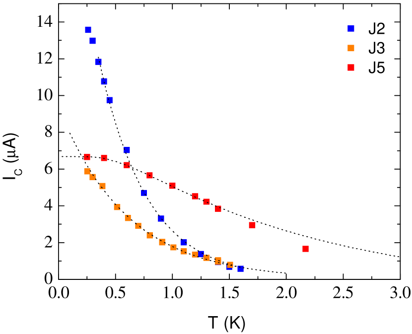
In order to provide an estimate of we measured vs. curves for all junctions. Three representative results (filled points) are shown in Fig.3. can be well approximated by an exponential function for sufficiently long junctions and high temperatures ():
| (1) |
where is linked to the Thouless energy of the system by dubos . We have used Eq. 1 to fit our data for all junctions of type A and B as shown in Fig.3. The resulting values of are reported in Table 1. For these devices is smaller than , which can be calculated from the relevant diffusion coefficients and junction lengths.
The values of the ratio span from 60 to 170 and for all junctions in the temperature range considered in the fit (mK), fully justifying the use of Eq. 1 dubos . Our analysis of vs. shows that type A and B junctions exhibit a behavior characteristic of much longer junctions with respect to their actual geometric length. vs. corresponding to junctions of type C is remarkably different from those of other devices as shown in Fig.3. The curve is concave downward and saturates at 250mK. This curve shape is typical of junctions having SN interfaces with low barrier resistance (see Figure 6 in ref. Hammer2007, ). For these devices in the whole temperature range considered (low temperature regime) dubos ; Hammer2007 , can be approximated by dubos ( is for J5). An excellent fit is achieved with an effective Thouless energy of and parameters , . The quality of the fit, slightly deviating from the experimental data only for , confirms that the value of is comparable to as opposed to cases A and B. This suggest that the nature and/or the geometry of super/semi interface characterizing type C can yield a higher effective Thouless energy.
The reasons for which Type C interfaces have better performance are not quite clear but are probably originated by a different structure following the peculiar fabrication procedure. This last includes Ti mask deposition, reactive ion etching, and mask removal by HF solution. In this configuration an etched wire of small width (450nm) is in contact with the superconductor not only on the top of the smooth mesa surface, like in cases A and B, but also through the two sides, at the rough surface of the etched side walls. It is however not possible to ascribe with certainty the improvement of the interface to the top contact, to the side contact or both. It is widely accepted that the relatively poor quality of S/N barriers is largely determined by reactive ion etching. Yet this is funded on data for junctions whose SN side contacts were taken on buried two dimensional electron gases IcQuant ; schapers98 . In those devices contacts were made to the side of active layers less than nm thick, which were charge populated by modulation doping. Our junctions are based on bulk doped surface layer and are therefore quite different from most systems studied in literature. Bulk doped structures like ours are more robust, as compared to modulation doped quantum wells, to the formation of a charge depleted (dead) layer at the two sides of the mesa after dry etching. We believe that the rough surface of the side walls (which is still perfectly conducting in our case) promotes the adhesion of metallic films thus improving effective contact area, and transparency. An inhomogeneous contact can present areas with different transparency: indeed the overall behavior of the junction is determined by those areas having a large transparency. Another mechanism worth future investigation is a possible change in the chemistry of the top surface in the epilayer due to deposition and subsequent removal of the Ti mask. A chemical reaction at the surface between the mask and the semiconductor could be favored, for instance, by local heating of the mask during the RIE.
In Tab. 1 we calculate theoretical expected for J1-J6 after Ref. dubos, on the basis of . We find for all junctions, including J5 and J6, a factor that is around two between theoretical and measured notaRn . This confirms the effectiveness of the model described in ref. Hammer2007, . Our data systematically show for the first time that SNS systems with non ideal SN interfaces can be characterized by an energy scale () capable to account for barrier resistance and transport parameters simultaneously. The other interesting result is the identification of a fabrication process for which is almost equal to (J5 and J6). The agreement of with existing theory is not perfect for both high transparency junctions (J5 and J6), and low transparency Junctions (J1-J4). A discrepancy with theory of the same order was also found in some works based on metallic SNS junctions Angers ; courtois and attributed to spurious factors like the effective area of the contact dubos .
Finally we note that J5 and J6 exhibit an value very close to the maximum obtainable for the given geometry and material parameters for ideally transparent interfaces. To the best of our knowledge similar results for semiconductor/superconductor devices were obtained only for junctions employing Si/Ge tinkham and InAs nanowires doh07 . We remark that, differently from the last two cited works, our devices are based on a standard top-down fabrication approach fully compliant with large scale integration. We stress that J5 and J6 were fabricated on different samples in different time. For J6 HF cleaning was more concentrated (1/20 instead of 1/50) and the normal conductor was ring shaped. To calculate the supercurrent density for J6 we considered as the sum of of the width of the two arms forming the ring. For the estimation of the Thouless energy we considered equal to one half the average circumference of the ring plus the gap between Nb electrodes and the ring. High values of the characteristic voltage have been obtained on similar structures produced with the same fabrication process. These are mostly SNS junctions having ring shaped normal conductor. Further details on SNS ring devices will be reported elsewhere.
In conclusion we showed that the quality of semi/super interface does play a crucial role in determining the value of the effective Thouless energy in SNS junctions. The comparison of different junction architectures shows that the reduction of is accompanied/mediated by the reduction of effective Thouless energy. We determined a junction configuration maximizing and supercurrent density. This opens the way to the realization of charge-controlled devices (J-dot) with critical currents larger than nA.
We acknowledge useful discussions with A. Golubov, A. Tagliacozzo and P. Lucignano. Financial support from EC within FP6 project HYSWITCH (FP6-517567) is acknowledged.
References
- (1) G. E. Blonder, M. Tinkham, and T. M. Klapwijk Phys. Rev. B 25, 4515 (1982)
- (2) H.Takayanagi, T. Akazaki, and J. Nitta Phys. Rev. Lett. 75, 3533 (1995)
- (3) J. van Dam, Y. Nazarov, E. Bakkers, S. De Franceschi, L. Kouwenhoven, Nature 442, 667 (2006).
- (4) K Grove-Rasmussen, H Ingerslev J rgensen and P E Lindelof 2007 New J. Phys. 9 124
- (5) Y-J. Doh, J. A. van Dam, A. L. Roest, E. P. A. M. Bakkers, L. P. Kouwenhoven, and S. De Franceschi, Science 309, 272 (2005).
- (6) F. Giazotto, P. Pingue, F. Beltram, M. Lazzarino, D. Orani, S. Rubini, and A. Franciosi Phys. Rev. Lett. 87, 216808 (2001)
- (7) The few works that make exception to this are mainly based on very short junctions
- (8) A. Chrestin and U. Merkt Appl. Phys. Lett. 70-23 1997
- (9) Th. Schäpers, J. Malindretos, K. Neurohr, S. Lachenmann, A. van der Hart, G. Crecelius, H. Hardtdegen, H. Lüth, and A. A. Golubov Appl. Phys. Lett. 73, 2348 (1998)
- (10) J. P. Heida, B. J. van Wees, T. M. Klapwijk, and G. Borghs Phys. Rev. B 57, R5618 (1998)
- (11) K. W. Lehnert, N. Argaman, H.-R. Blank, K. C. Wong, S. J. Allen, E. L. Hu, and H. Kroemer Phys. Rev. Lett. 82, 1265 (1999)
- (12) T. D. Clark, J. Appl. Phys. 51 (1980) 2736
- (13) V.Z. Kresin, Phys. Rev. B 34, 7587 (1986)
- (14) M. Yu. Kuprianov and V.F. Lukichev, Sov. Phys. JETP 67, 1163 (1988)
- (15) J.C. Hammer, J.C. Cuevas, F.S. Bergeret, W. Belzig Phys. Rev. B 76, 064514 (2007)
- (16) F. Capotondi, G. Biasiol, D. Ercolani, V. Grillo, E. Carlino, F. Romanato, and L. Sorba, Thin Solid Films 484, 400 (2005).
- (17) P. Dubos, H. Courtois, B. Pannetier, F. K. Wilhelm, A. D. Zaikin, and G. Schön, Phys. Rev. B 63, 064502 (2001).
- (18) J. Gu, W. Cha, K. Gamo, and S. Namba, J. Appl. Phys. 50, 6437 (1979).
- (19) In geometry “A” normal current can flow outside the close inter electrode area, where supercurrent is confined, leading to a reduced value of . Due to the favorable value of the ratio the understimate of is a small percent.
- (20) L. Angers, F. Chiodi, G. Montambaux, M. Ferrier, S. Gueron, H. Bouchiat, J. C. Cuevas, Phys. Rev. B 77, 165408 (2008)
- (21) H. Courtois, Ph. Gandit, and B. Pannetier, Phys. Rev. B 52, 1162 (1995)
- (22) ie Xiang, A. Vidan, M. Tinkham, R. M. Westervelt, Charles M. Lieber Nature Nanotechnology 1, 208 - 213 (05 Dec 2006)