Electrical rectification effect in single domain magnetic microstrips: a micromagnetics-based analysis
Abstract
Upon passing an a.c. electrical current along magnetic micro- or nanostrips, the measurement of a d.c. voltage that depends sensitively on current frequency and applied field has been recently reported by A. Yamaguchi and coworkers. It was attributed to the excitation of spin waves by the spin transfer torque, leading to a time-varying anisotropic magnetoresistance and, by mixing of a.c. current and resistance, to a d.c. voltage. We have performed a quantitative analysis by micromagnetics, including the spin transfer torque terms considered usually, of this situation. The signals found from the spin transfer torque effect are several orders of magnitude below the experimental values, even if a static inhomogeneity of magnetization (the so-called ripple) is taken into account. On the other hand, the presence of a small non-zero average Œrsted field is shown to be consistent with the full set of experimental results, both qualitatively and quantitatively. We examine, quantitatively, several sources for this average field and point to the contacts to the sample as a likely origin.
pacs:
72.25.Pn, 76.50.+g, 41.20.-q, 72.15.-vI Introduction
The possibility to act on the magnetization of a sample by an electrical current within it, not through the classical Œrsted field but through the spin-polarization of electrical current in ferromagnets, offers fascinating opportunities in nanomagnetism and nanoelectronics Berger (1996); Slonczewski (1996). In the situation where the sample consists of separated and uniformly magnetized media crossed by the current, the description of the physics appears simpler and, indeed, agreement between experiments and modelling does not appear out of reach Krivorotov et al. (2005); Berkov and Miltat (2008). However, when the current flows in a magnetic medium with a continuously varying magnetization, the situation is more complex. As a result, several forms for this so-called spin transfer torque (STT) have been proposed Bazaliy et al. (1998); Thiaville et al. (2004); Zhang and Li (2004); Thiaville et al. (2005), and the appropriate equation for magnetization dynamics has even been questionned Stiles et al. (2007); Smith .
In such a situation, the more experimental results in different configurations is clearly the better. Among these, the recent discovery of an electrical rectification effect in magnetic strips with widths of the order of a micrometer and thicknesses of the order of a few tens of nanometers Yamaguchi et al. (2007) is especially appealing. The effect was observed for current densities below or of the order of those required for STT to act on domain walls. However, a relatively large static field was applied so that the strip was in a single domain state, contrarily to the situation where a signal was measured in presence of a domain wall Bedau et al. (2007); Moriya et al. (2008). This last feature is puzzling. Indeed, STT within a continuous magnetization structure is only expected when a magnetization gradient exists. In the simplest STT formulation, valid for slow magnetization variations with respect to electrons’ spin precession or diffusion length, the STT is namely expressed as
| (1) |
where the velocity is an expression of the current density with spin polarization according to
| (2) |
The (small) number has been related to spin flip of the conduction electrons, in several models Zhang and Li (2004); Thiaville et al. (2005); Tatara et al. (2007); Piéchon and Thiaville (2007). From (1), one sees that magnetization gradients along the electric field are required. Such gradients should however not exist in the experimental situation considered above (long strip under a large field), at least for perfect samples. The possibility mentioned by the authors is that the uniform state becomes unstable under a.c. current at an appropriate frequency, as indeed predicted for very large d.c. currents Shibata et al. (2005).
The object of this paper is to perform a full micromagnetic analysis of the situation in order to analyze the various sources of rectification signal discussed above, and to quantitatively compare the calculated signals with the experimental results.
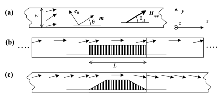
The experimental conditions Yamaguchi et al. (2007) are as follows (see Fig. 1 for notations): the sample is a magnetic strip, several micrometers long with various widths (from 300 to 5000 nm) and thicknesses (30 to 50 nm), with the experimental constraint of a close to 50 resistance; a magnetic field is applied in the sample plane, at an angle ; an a.c. current with swept frequency is injected into the sample through a coplanar waveguide; current densities are of the order of 1010 A/m2 i.e. low compared to those required for domain wall displacement Kläui et al. (2005). The experimental results may be summarized by: a d.c. voltage is measured with a marked frequency dependence, it becomes important (V) only at a well defined frequency of the order of the ferromagnetic resonance frequency; the position of the resonance is strongly influenced by the field magnitude (in accord with Kittel’s law); the d.c. voltage increases as the square of the injected current; the angle dependence of the d.c. voltage is well described by a law at large fields, turning to at low fields.
Our approach uses both analytical and numerical micromagnetics: we solve the Landau-Lifchitz-Gilbert magnetization dynamics equation with incorporation of the two basic STT terms (1). Section II is devoted to the case of a uniform magnetization along the strip axis, where no STT is expected in the linear limit. The next section introduces structural inhomogeneities, in the spirit of the well known ripple patterns in thin films Hubert and Schäfer (1998), so that a STT is present in the ground state. As both configurations lead to d.c. voltages much below the experimental levels, Sec. IV investigates the effects of a small average Œrsted field. Finally, as the samples have been carefully designed to avoid fields from the current leads, an intrinsic origin to this field from different electron scattering properties at the top and bottom surfaces of the strip is discussed.
II Uniform magnetization
We first look at the simplest situation where the magnetization does not change in the direction of the electric field, at least in the rest state without current.
II.1 Analytical analysis of the uniform situation
The magnetization at rest will be denoted , with . In the presence of the a.c. current, a small deviation appears (). The current is described by a spatially uniform that is harmonic in time with pulsation . With the axes defined in Fig. 1 one has . The LLG equation supplemented by both STT terms reads, to first oder in the deviations
| (3) | |||||
In this equation, is the effective field of the static magnetization (with by definition) and is the effective field resulting from the existence of the deviation , with contributions from the exchange and magnetostatic energies. With only the first two terms on the right-hand side of (3), upon diagonalization, the various spin wave modes corresponding to the static magnetization are obtained Bayer et al. (2006). Their amplitude is fixed by the thermal noise. The last two terms represent the spin-wave pumping by the STT. We note that they have the form of a product (we forget the spatial derivatives here as the argument is about the time dependence). Therefore, if varies in time with the pulsation also, these terms do not contribute to as they lead to pulsations and .
In fact, a coupling of the form is known to give rise to parametric excitation, i.e. the generation of a solution at frequency by pumping at frequency . Parametric pumping of spin waves from a uniform starting configuration would not be in agreement with the experimental results (point ), since the resonant frequency found for the current is of the order of the FMR frequency, not twice this value.
II.2 Numerical calculations
As analytical calculations suffer from some limitations, such as linearization and the consideration of simple structures only, they were completed by full micromagnetic numerical simulations (see Methods in Ref. Nakatani et al. (2003)). These were performed by solving the LLG equation with the STT terms. The typical velocity equivalent to the current applied was m/s (corresponding to the experimental current density A/m2 with a polarization ). In addition, for the purpose of showing better the effect of STT, values of as large as 100 or even 1000 m/s were applied. As no effects of the term were observed (this will become clear from the analytical calculations), the results shown below were obtained with . We will throughout the paper show results for just one sample size (width nm and thickness nm), i.e. values corresponding to one sample of Ref. Yamaguchi et al. (2007). Material parameters were those representative of Ni80Fe20, namely magnetization kA/m, exchange energy constant J/m, no crystalline anisotropy (except for the ‘ripple’ case, see Sec. III), gyromagnetic ratio m/(As) and damping parameter . A static field was applied in the sample plane, at an angle , with standard values mT and (the value where the d.c. signal is close to maximum). The calculation region length , a part of the real sample length , was taken to be m, mostly (calculations with or 4 m were also conducted for the purpose of checking the dependence on of the d.c. voltage). The mesh size was nm3 mostly. The d.c. voltage was computed from the time variation of the anisotropic magnetoresistance (AMR) of the sample. Denoting the resistivity change upon magnetization rotation by (with, for the used NiFe alloy at room temperature, m), the dependence of the wire resistance upon its magnetization distribution is expressed as
| (4) |
where is the wire cross-section area () and denotes the average over the calculation region.
Note that, as there is no domain wall in the calculation region and a field with a transverse component is applied, the calculation scheme has to be different from that used for the simulation of domain wall dynamics Nakatani et al. (2003): one cannot assume that outside the calculation region the magnetization is uniform and equal to . Thus, the calculation region was embedded in a wire of infinite length according to two different models (too simple embedding schemes can lead to gradients of in the direction, that cause large spurious spin transfer torques). In the ‘periodic’ model (Fig. 1b), the calculation region is supposed to be repeated periodically in the direction. The exchange and demagnetizing fields are calculated accordingly, as well as the gradients for the STT. The current density is uniform. In the ‘infinite’ model (Fig. 1c), one assumes that the values at the left edge of the calculation region extend to infinity on the left side, and similarly on the right. The boundary conditions at left and right are free. The demagnetizing field takes into account these two semi-inifinite regions. In order to avoid end effects, the current density is zero at and rises (along a length ) linearly towards the set value at the center of the calculation region.
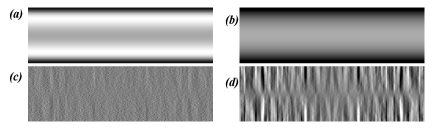
As seen in the analytical analysis (Sec. II.1), no effect is expected in first order perturbation as the initial state magnetization has no gradient along the current direction. Numerically however, the avoidance of any gradient is impossible, as this would require an infinitely precise numerical evaluation of the demagnetizing and exchange fields. It follows that, depending on the model used and the accuracy of the numerical scheme, a gradient along of the magnetization remains that gives rise to a non-zero STT, therefore to a magnetization oscillation and finally to some d.c. voltage. The most uniform initial state was obtained with the infinite model, and is depicted in Fig. 2 for a field applied at . Note that, as the field is inclined and its value mT is below the effective transverse anisotropy of the magnetic strip, the magnetization becomes non uniform in the transverse direction, with more rotation towards the field at the strip center. Fig. 2 proves that the non uniformity in the direction of the magnetization is essentially due to the numerical precision of the calculations (a double precision number is described with a relative precision of ).
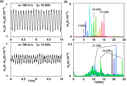
The time variation of the magnetization at position in the calculation region, under a.c. current at various frequencies, is plotted in Fig. 3 for the initial state depicted in Fig. 2. The current amplitude was m/s, much higher than the largest experimental value ( m/s), but this was necessary in order to see some effect. Indeed, the deviations of this central moment are extremely small, of the order of 10-15 whereas the initial value is at that point. The Fourier analysis of the data reveals that the fundamental frequency of the a.c. current is seen in the spectra only when it is close to a resonant frequency of the sample (the numerical calculation of the FMR-like excitation of the sample by an a.c. field in this configuration shows resonance at GHz). In this regime, multiples of the fundamental frequency are also seen. In addition, when is close to twice this resonant frequency, a (broader) response at half the current frequency can be seen. This is a characteristic of the parametric excitation, expected from the analytical analysis presented above.
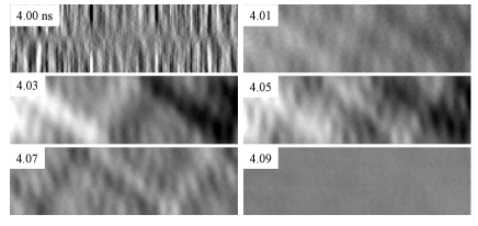
In order to see how this oscillation behaves in space, some snapshots of the magnetization structure are provided in Fig. 4. The images reveal that the complex wavy state seen in the structure at rest (Fig. 2) acquires a tiny oscillation in the form of a quasi-standing wave pattern (with some very geometrical features that may be artifacts). Such a pattern had been evidenced in the preliminary calculations Yamaguchi et al. (2007, ). However, the amplitude of this oscillation is extremely small (in cases where the gradients of static magnetization at the left and right edges of the calculation region are less carefully avoided, the oscillations are stronger).
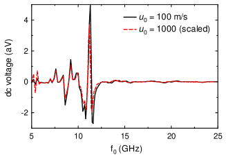
Therefore, the computed d.c. voltages are, even at their maximum around the FMR frequency, orders of magnitude (here, ) below the experimental values, as shown in Fig. 5. Thus, clearly, another mechanism has to be found.
III Non uniform magnetization
The analysis in the preceding section has shown that one of the reasons for the absence of signal was that the initial state contained no gradient along the electric field. A well-known cause for such non uniformitiy is the so-called ‘ripple’ pattern Hubert and Schäfer (1998), a result of a random distribution of anisotropy in crystallites. The response of the magnetization structure to this random potential is to organize itself in ripple domains, where the magnetization deviates slightly from its average value in one direction or the other. These domains have a characteristic lens shape, with the long axis of the lens oriented normal to the magnetization. The presence of the ripple structure is attested by Lorentz electron microscopy (see e.g. Ref. Fuller and Hale (1960)).
III.1 Analytical model for smooth ripple
A first model consists in assuming that the ripple pattern can be described by a smooth undulation of the magnetization. Thus we write , where oscillates, more or less regularly, in space. The small deviation is decomposed into an in-plane component and an out-of-plane component: , where is the unit in-plane vector orthogonal to the local magnetization and the unit vector normal to the film plane. The linearized LLG equation projected on these two vectors now reads
| (5) |
To solve the equation, we assume that the two components of the effective field are simply proportional to the magnetization deviations : and . For a thin fim, one expects that if the ripple period is much larger than the sample thickness. The term corresponds to the effective potential that stabilizes the value of and its variation with . The equations are linear and contain the STT as a driving term now. They are easily solved in the harmonic approximation : , and . We then get
| (6) |
The magnetization in-plane deviation becomes large at the ferromagnetic resonance defined by . As the meaning of the deviation component is a rotation of the in-plane magnetization angle , we see that at resonance a current transforms the structure as
| (7) |
This means that the ripple magnetic pattern under STT is set into oscillation along the direction. The amplitude of oscillation at resonance is typically (in the thin film approximation where )
| (8) |
For m/s, the oscillation amplitude computed from (8) is nm.
The predicted oscillation of the ripple pattern is therefore quite small. Moreover, in an infinite wire, the modulation of the total anisotropic magnetoresistance is exactly zero, as the structure is merely translated. For a wire of finite length, some small signal can be expected as, at both ends, some part of the structure disappears or appears because of the structure oscillation in position. In such situation however, the sign of the d.c. voltage should be arbitrary and the d.c. voltage magnitude should not depend on sample length.
III.2 Numerical calculations
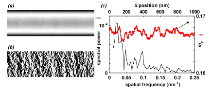
As for the preceding section, numerical calculations were performed in order to get quantitative results. For inducing a ripple structure, a random anisotropy field was introduced, with a fixed value and a random in-plane easy axis orientation. Results obtained for mT only will be shown here. The description of the magnetic structure at rest is provided in Fig. 6, to be compared to that of the perfect sample (Fig. 2). It is clear that the random anisotropy leads to much larger magnetization deviations than the residual ones in the perfect case. The structure evidences some periodicity along (about 250 nm, see a profile of in the direction together with its Fourier transform in Fig. 6c). In the ripple theory Hubert and Schäfer (1998), two structural periods appear, that in the direction of magnetization being consequently smaller than that in the orthogonal direction. This larger period appears to be mostly suppressed by the reduced width of the nanostrip sample, for the parameters chosen here. Note the similarity of the differential magnetization image in Fig. 6b with typical TEM images in Lorentz mode, that also depend on magnetization gradients Fuller and Hale (1960).
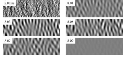
Under application of an a.c. spin polarized current, the magnetization structure is driven into some oscillation. Fig. 7 provides some snapshots of the magnetization distribution, for the high current amplitude m/s. Despite the large current, the oscillation nature is hard to apprehend from the movies of . Therefore, the time differentials were drawn. The component of was chosen as it is the most labile, the magnetization at rest under the applied field being close to the direction, in the standard case illustrated here. A very smooth modulation appears, that contrasts with the noisy appearance of the rest state gradient image. It is a standing wave pattern tuned to the current frequency (this pattern is already discernable in Fig. 4 behind the more geometrical texture). Note that the wave pattern is not exactly ‘standing’: the modulation breathes with time but also deforms slightly during one period. This deformation looks like the pattern oscillation computed in the previous subsection, but this requires a more precise verification. The ‘wavevector’ of this pattern is roughly parallel to the direction, and the wavelength is decreasing as the applied frequency increases (not shown). This last feature, compared to the conclusions of the previous subsection, shows that the dominant mechanism of the spin transfer torque action is different.
A more appropriate description can be constructed by assuming that the ripple pattern is random. The spin transfer torque due to the gradients of the structure at rest is equivalent to a field that ‘pumps’ the deviations , expressed as
| (9) |
Note that Fig. 6b can also be seen as displaying the largest component of this field. Therefore, in first approximation, this field is random in space but perfectly harmonic in time. By Fourier transformation, this field can excite spin wave modes with a frequency matching the current frequency and a wavevector contained in the spectrum of . Thus, the field is similar to the thermal field that gives a non zero amplitude to the thermodynamic spin waves (as seen in Brillouin scattering), with the only difference that instead of being white in temporal frequency it is monochromatic. Therefore, the observation of induced spin wave modes is no surprise. From the analogy with the thermal field we get that the amplitude of the spin wave is proportional to current (and also to the strength of the ripple ).
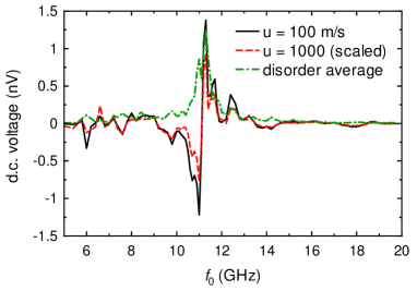
The next question concerns the detection of this induced spin wave as a d.c. voltage. In first approximation, the wavelength of the standing spin wave pattern ( nm at 11 GHz here) being much smaller than the length of the sample, the variation of the total AMR averages to zero. However, as the standing wave pattern is not perfect, being deformed by the ripple structure (see Fig. 7), the average is not perfectly zero. It is a random number with a typical value times smaller than the local amplitude. Fig. 8 shows a spectrum calculated for one particular realization of the ripple. A resonance appears (with a close to expected shape for that spectrum) at GHz, i.e. the FMR frequency of the sample, meaning that the uniform mode is also pumped by . The values are much larger than in the nominally uniform case studied earlier (Fig. 5) and a large irregularity is present, a signature of the randomness of the averaging over the sample size. To this curve is superposed the average of the absolute values of the d.c. voltages calculated for 16 realizations of the ripple. Furthermore, a calculation run for a m calculation length and m/s gives a similar result, as expected (not shown). Finally, the voltage is found to be proportional to the square of the a.c. current, as expected from the proportionality of spin wave amplitude to current (compare the scaled spectra in Fig. 8 for and m/s). This has the consequence that, for current amplitudes similar to the experiments, the calculated d.c. voltage should be smaller by a factor 1000, i.e. a million times smaller than what is measured. Therefore, we conclude that the ripple hypothesis is also not able to account quantitatively for the measured rectification signal.
IV Effect of a parasitic field
The analysis of the first sections has shown that virtually no rectification effect is to be obtained through a STT as described in (1), in a single domain ferromagnetic wire. Of course, we cannot exclude that other mechanisms than those already investigated play a role in the interpretation of the experiments, but we need also to investigate the effect of mechanisms competing with STT. In the following, we examine the influence of a parasitic Œrsted field on the rectification effect.
If we consider an infinitely long wire with a uniform current density, the average value of the Œrsted field is zero. As the wire has a flat cross-section, the largest components of the field are vertical ( direction) and are found at the two lateral edges of the wire. For the nm2 wire submitted to a current density A/m2, the maximum vertical field is equal to mT (the horizontal components reach mT). These fields, normal to the magnetization at rest, excite magnetization oscillations in the vicinity of the wire surfaces. What will be the impact on the sample resistance ? As a static field is applied in the sample plane, at angle from the wire axis, the component at rest is not zero. In presence of the Œrsted field, this component oscillates and therefore the AMR is modulated. However, as the fields have opposite signs at two opposite surfaces, the total AMR modulation should cancel by integration.
Note that, in principle, the cancellation may be incomplete. For example, in the spin-wave community, the effect of interfaces is often taken into account by a pinning length such that the boundary condition for the oscillating magnetization is
| (10) |
where denotes the coordinate normal to the interface Rado and Weertman (1959); Guslienko and Slavin (2005). The original condition Rado and Weertman (1959) specified that , with the surface anisotropy constant, but recently magnetization oscillation profile calculations were shown to be explainable through a pinning length related to the sample dimensions Guslienko and Slavin (2005), actually a pure magnetostatic effect. Here, whereas there is no reason to have any dissymetry between opposite surfaces for magnetostatics, a chemical or structural difference between the top and bottom surfaces of the magnetic film cannot be ruled out, leading to different surface anisotropies. It is obvious that this will result in a non zero AMR oscillation and, therefore, a non zero d.c. voltage at the resonance frequency of this perpendicular standing spin wave mode (PSSW). Generally, the frequency of the PSSW is different from that of the uniform FMR mode, allowing their discrimination. Indeed, on the one hand, frequency should increase due to exchange. But, on the other hand, the transformation of the lateral magnetostatic dynamic charges from monopolar to dipolar decreases the dynamic demagnetizing field, thus reducing the frequency. In the case at hand, the direct numerical calculation gave 10.6 GHz for the PSSW, close to the value of 11 GHz for the uniform mode, so that a frequency discrimination is not possible. Turning now to the signal levels, an upper bound to this contribution can be obtained by evaluating the d.c. voltage on one half of the sample thickness. As peak values of V were obtained, we conclude that the d.c. voltage due to a perfect Œrsted field is not sufficient, by a factor , to explain the experimental results Let us therefore now suppose that the average of the Œrsted field is not exactly zero.
IV.1 Analytical model with a.c. field excitation
We assume here that the magnetization is uniform (in-plane angle ) so that from (4) the total AMR is . When the magnetization angle is oscillating as , with , the sample resistance change due to AMR, for a sample of length , reads
| (11) |
where . We now determine the angle oscillation . The equations of motion use the same variables as in Sec. III.1, but now instead of considering the STT we include an a.c. field (this represents a general non-zero average for the Œrsted field due to the current, and neglects the zero average part). The LLG equations of motion now read
| (12) |
The harmonic solution (with etc.) reads similarly
| (13) |
At resonance, taking into account that , the amplitude is approximately (note that the field gives the largest effect)
| (14) |
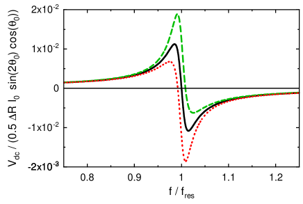
As this variation of magnetization does not change sign over the sample, it will not average to zero by integration. Consequently, this magnetization oscillation produces an oscillation of the sample resistance at frequency , from which a d.c. voltage results. The d.c. voltage has a peak close to the resonance frequency : as the phase of is close to the signal is zero at resonance but has peaks of alternating signs on both sides (as in the experiments Yamaguchi et al. (2007)). The typical d.c. voltage is thus
| (15) |
With this formula we see that, as in the experiments, the voltage is proportional to the current square (as the Œrsted field is proportional to the current), and that the dependence on magnetization angle conforms to the law. Fig. 9 displays the frequency dependent d.c. voltage evaluated from (11, 13). The d.c. voltages are of the order of the micro-Volt, like in the experiments. With a sole a.c. field in the direction, an antisymmetric line shape is obtained, whereas an a.c. field contributes with a symmetric line shape. Therefore, the experimental line shapes Yamaguchi et al. (2007) may be interpreted by a combination of both of these fields.
We conclude analytically that a non-zero Œrsted field provides a plausible explanation of the experimental results showing a rectification effect in nano and microstrips. This was qualitatively stated in Ref. Yamaguchi et al. , but dismissed on the ground that the average field should be zero. The last section of this paper will therefore study possible origins for such fields.
IV.2 Numerical calculations
The influence of the Œrsted field was investigated by numerical calculations also. Indeed, the magnetization non uniformity in the transverse direction, as a function of applied field angle and magnitude, or the evaluation of the effect of the full Œrsted field, require a micromagnetic simulation.
For the latter point, calculations with a variation along the axis are not essential. Thus, for the description of the full Œrsted field in the sample cross-section and the calculation of the resulting d.c. voltage, a 2D model (, ) with invariance in the direction was also employed. The case with no bias (for or ) was already discussed. When a bias is added, we find that the d.c. voltage spectra are affected by the presence of the full Œrsted field only at the frequency of the PSSW, with a minor quantitative influence when the d.c. voltage is computed on the full sample thickness. Therefore, we kept the model used in the rest of the paper for the other calculations with a.c. field, and neglected the full Œrsted field whose average is zero.
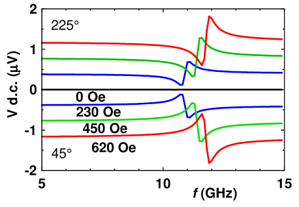
First, an a.c. field with component only was considered with an amplitude mT. The dependence of the d.c. voltage spectra on the static field value, for two opposite field directions, is illustrated in Fig. 10. The field values and angles, as well as the current density, were chosen to match those of the experiments Yamaguchi et al. (2007). In comparison to the analytical calculation assuming uniform magnetization (Fig. 9), the signal is roughly divided by 2. The results are very similar to experiments, qualitatively and quantitatively (the computations apply to a calculation region 1 m long whereas for these dimensions and the nominal resistivity of NiFe the sample length corresponding to 50 is 3 m), with only a difference in the peak shape. However, from the analytical modeling (see Fig. 9) we know that such change of shape can be obtained by adding a component to the a.c. field.
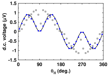
Another important experimental feature is the dependence of the d.c. voltage peak to peak amplitude on the applied field angle. It was analytically shown above that the observed behaviour (the law) was expected for an a.c. field. The numerical results substantiate this conclusion, as shown in Fig. 11 for two values of the static applied field. For the large value ( T), the magnetization angle follows the field angle closely and the law is well obeyed. For the smaller field ( T), closer to the shape anisotropy field of the nanostrip, an evolution towards a variation is evident.
Therefore, assuming that a non zero average Œrsted field exists, we have been able to reproduce all experimental results, quantitatively with a.c. fields mT. This is in sharp contrast with the alternative explanations based on STT, that result in rectification signals that are orders of magnitude smaller.
V Possible origins for a parasitic field
The question now arises naturally about the origin of such a non zero average field. We note that the design of the electrical connections to the magnetic wire in the experiments Yamaguchi et al. (2007) was very symmetrical, the sample being inserted in a coplanar waveguide with a ground-signal-ground structure. This ensures geometrically that the Œrsted field applied to the sample in the presence of a current is minimized. Of course, any imbalance in current backflow between the 2 ground leads, or imperfect centering of the sample, creates an a.c. field (for example, we estimate roughly that a 1 % imbalance would give T ). However, there are two different reasons for which a non-zero average component of this field can still exist: (i) the gold coplanar waveguide (100 nm thick) contacts the magnetic sample by its top surface; (ii) due to differences in the top and bottom interfaces of the magnetic film, the current distribution could be non uniform, even in an infinitely long magnetic strip. We try now to estimate these fields.
V.1 Field from current distribution in the sample thickness
We first assume that neither a non magnetic conductive underlayer nor overlayer exist (that would obviously give rise to a field), and look for an intrinsic origin for a non uniform current distribution. For the description of electronic transport in thin metallic films, the Fuchs-Sondheimer model Sondheimer (1952) evaluates the current distribution in the thickness of a thin film, within a Boltzmann equation approach. A key parameter introduced in this model is the specularity parameter at every interface: means that electron reflection at the interface is perfectly specular and that it is random. In the latter case the current is reduced at the interface. The characteristic scale (in ) over which this reduction extends is given by the mean free path . Extending the Fuchs-Sondheimer calculation to different interfaces at the film top () and bottom () Lucas (1965), we obtain in the limit of a thick film () the following current distribution
| (16) |
where the function is an exponential integral
| (17) |
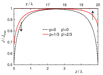
Two profiles of the current for the case nm and a mean free path nm are plotted in Fig. 12. The cases , and , are compared. In the former, the current density is reduced to one half at both interfaces, symetrically. In the latter, the current is reduced to at one interface and to at the other, so that becomes asymmetric.
The next step is to evaluate, from this asymmetric current distribution, the average Œrsted field within the sample. As is asymmetric in , this gives rise to a non zero average for the field component transverse to the strip axis (). The analytical calculation of this average field shows that the contribution of a current layer at depth to the average field is very close to linear, the contribution being zero for . In other words, the field average over and is
| (18) |
where is a number equal to in the limit and amounting to for the sample we consider here with . From (16) and (18) we obtain for A/m2, nm and nm, T. This value could be perhaps doubled by taking a longer mean free path and increasingly different specularity parameters, but remains too low for explaining the experiments.
V.2 Field from the contact regions
In the lack of a full 3D current distribution calculation, the typical field due to the gold electrodes being deposited on top of the strip surface can be evaluated roughly. We assume that, at both ends of the magnetic strip (length ), the current flows vertically between the magnetic strip and the gold electrodes, the latter being twice as thick and 10 times more conductive than the magnetic sample. The length of this vertical part is taken to be the thickness of the magnetic layer. At the center of the magnetic strip, considering that , the resulting typical field reads
| (19) |
With A/m2, m, nm and nm, one gets T. Thus the central value of this field is also too low with regard to the experiments. However, it becomes much larger close to the contacts. For the average value of the field over the full sample ( and ), we obtain
| (20) |
(in order to remove a divergence we assume that the current flows vertically over a length along the axis at the contacts). The same numbers now give mT, a value compatible with those explaining the d.c. voltages experimentally measured. Therefore, we propose that the rectification signals are due to this field. It should be noted that this field decreases as the inverse of the sample length, in contrast to the intrinsic mechanism whose the contribution is independent of sample length.
VI Conclusion
This work has tried to reach a quantitative description of the spectra of d.c. voltage versus frequency obtained on nanostrips subjected to a static in plane field. We have found that, for a perfect wire, no signal should be expected owing to a linear analysis. The consideration of internal magnetic inhomogeneities in the nanostrip (ripple structure) do lead to non zero rectification voltages. However, these are disorder dependent and much too low compared to experimental findings. As a solution to this paradox, we tested the influence of a non zero average value of the Œrsted field generated by the a.c. current, and found that small values (0.1 mT) of this average lead to quantitative agreement with experimental findings. We propose two origins for these fields. The extrinsic one is due to the contacts put on the magnetic sample (as considered recently in the case of vortex excitation by a.c. currents Bolte et al. (2008)). The intrinsic one is due to an asymmetric current distribution in the thickness of the magnetic nanostrip. In the semi-classical description by Fuchs and Sondheimer of the conductivity of very thin films, such an asymmetry results from different specularity parameters for electron reflection at the top and bottom surfaces of the magnetic layer.
Therefore, we conclude that Œrsted field effects should be carefully investigated when interpreting experiments by the spin transfer torque mechanism. The extrinsic contribution should be precisely evaluated, so that the numerical evaluation of the field taking into account the full sample structure may become mandantory in the future. The important role of small a.c. fields at resonant frequencies is not so surprising in fact: in ferromagnetic resonance, for a sample with like NiFe, the excitation field is of the order of T.
VII Acknowledgements
Comments by J. Miltat and Y. Suzuki are gratefully acknowledged. The research of A.T. was supported by the french ANR PNANO programme, (DYNAWALL project), the Programme pluriformations SPINEL of Université Paris-sud, and the european network MRTN-CT-2006-035327 SPINSWITCH. The work of Y.N. was supported partly by a grant-in-aid for scientific research in the priority area “Creation and control of spin current” from the Ministry of Education, Culture, Sports, Science and Technology, Japan.
Note added in proof : A. Yamaguchi, in a recent work Yamaguchi et al. (2008), comes also to the conclusion that a field effect is very probably the origin of the rectification signal. In addition, as source of the non zero average field, he proposes the deformation of the field pattern at high frequencies due to electromagnetic effects, the permittivity of the substrate being different from that of air.
References
- Berger (1996) L. Berger, Phys. Rev. B 54, 9353 (1996).
- Slonczewski (1996) J. Slonczewski, J. Magn. Magn. Mater. 159, L1 (1996).
- Krivorotov et al. (2005) I. Krivorotov, N. Emley, J. Sankey, S. Kiselev, D. Ralph, and R. Buhrman, Science 307, 228 (2005).
- Berkov and Miltat (2008) D. Berkov and J. Miltat, J. Magn. Magn. Mater. 320, 1238 (2008).
- Bazaliy et al. (1998) Y. B. Bazaliy, B. Jones, and S.-C. Zhang, Phys. Rev. B 57, R3213 (1998).
- Thiaville et al. (2004) A. Thiaville, Y. Nakatani, J. Miltat, and N. Vernier, J. Appl. Phys. 95, 7049 (2004).
- Zhang and Li (2004) S. Zhang and Z. Li, Phys. Rev. Lett. 93, 127204 (2004).
- Thiaville et al. (2005) A. Thiaville, Y. Nakatani, J. Miltat, and Y. Suzuki, Europhys. Lett. 69, 990 (2005).
- Stiles et al. (2007) M. Stiles, W. Saslow, M. Donahue, and A. Zangwill, Phys. Rev. B 75, 214423 (2007).
- (10) N. Smith, cond-mat/0706.1736.
- Yamaguchi et al. (2007) A. Yamaguchi, H. Miyajima, T. Ono, Y. Suzuki, S. Yuasa, A. Tulapurkar, and Y. Nakatani, Appl. Phys. Lett. 90, 182507 (2007).
- Bedau et al. (2007) D. Bedau, M. Kläui, S. Krzyk, U. Rüdiger, G. Faini, and L. Vila, Phys. Rev. Lett. 99, 146601 (2007).
- Moriya et al. (2008) R. Moriya, L. Thomas, M. Hayashi, Y. Bazaliy, C. Rettner, and S. Parkin, Nature Phys. 4, 368 (2008).
- Tatara et al. (2007) G. Tatara, H. Kohno, J. Shibata, Y. Lemaho, and K.-J. Lee, J. Phys. Soc. Jpn. 76, 054707 (2007).
- Piéchon and Thiaville (2007) F. Piéchon and A. Thiaville, Phys. Rev. B 75, 174414 (2007).
- Shibata et al. (2005) J. Shibata, G. Tatara, and H. Kohno, Phys. Rev. Lett. 94, 076601 (2005).
- Kläui et al. (2005) M. Kläui, C. Vaz, J. Bland, W. Wernsdorfer, G. Faini, E. Cambril, L. Heyderman, F. Nolting, and U. Rüdiger, Phys. Rev. Lett. 94, 106601 (2005).
- Hubert and Schäfer (1998) A. Hubert and R. Schäfer, Magnetic Domains (Springer Verlag, Berlin, 1998).
- Bayer et al. (2006) C. Bayer, J. Jorzick, S. Demokritov, A. Slavin, K. Guslienko, D. Berkov, N. Gorn, M. Kostylev, and B. Hillebrands, Spin Dynamics in Confined Magnetic Structures III (Springer, Berlin, 2006), pp. 57–104.
- Nakatani et al. (2003) Y. Nakatani, A. Thiaville, and J. Miltat, Nature Mater. 2, 521 (2003).
- (21) A. Yamaguchi, K. Motoi, H. Miyajima, and Y. Nakatani, cond-mat/0710.2172.
- Fuller and Hale (1960) H. Fuller and M. Hale, J. Appl. Phys. 31, 238 (1960).
- Rado and Weertman (1959) G. Rado and J. Weertman, J. Phys. Chem. Solids 11, 315 (1959).
- Guslienko and Slavin (2005) K. Guslienko and A. Slavin, Phys. Rev. B 72, 014463 (2005).
- Sondheimer (1952) E. Sondheimer, Adv. Phy. 1, 1 (1952).
- Lucas (1965) M. Lucas, J. Appl. Phys. 36, 1632 (1965).
- Bolte et al. (2008) M. Bolte, G. Meier, B. Krüger, A. Drews, R. Eiselt, L. Bocklage, S. Bohlens, T. Tyliszczak, A. Vansteenkiste, B. V. Waeyenberge, et al., Phys. Rev. Lett. 100, 176601 (2008).
- Yamaguchi et al. (2008) A. Yamaguchi, K. Motoi, A. Hirohata, H. Miyajima, Y. Miyashita, and Y. Sanada, Phys. Rev. B 78, 104401 (2008).