Status of the QPACE Project
Abstract:
We give an overview of the QPACE project, which is pursuing the development of a massively parallel, scalable supercomputer for LQCD. The machine is a three-dimensional torus of identical processing nodes, based on the PowerXCell 8i processor. The nodes are connected by an FPGA-based, application-optimized network processor attached to the PowerXCell 8i processor. We present a performance analysis of lattice QCD codes on QPACE and corresponding hardware benchmarks.
1 Introduction
The QPACE project is designing and building a novel cost-efficient computer that is optimized for LQCD applications. This research area has a long tradition of developing such computers (see, e.g., [1, 2]). Previous projects were based on system-on-chip designs, but due to the rising costs of custom ASICs the QPACE project follows a different strategy: a powerful commercial multi-core processor is tightly coupled to a custom-designed network processor. The latter is implemented using a Field Programmable Gate Array (FPGA), which has several distinct advantages over a custom ASIC: shorter development time and cost, lower risk, and the possibility to modify the design of the network processor even after the machine has been deployed.
The development of QPACE is a common effort of several academic institutions together with the IBM research and development lab in Böblingen (Germany). First prototype hardware is already available and currently being tested.
2 The QPACE architecture
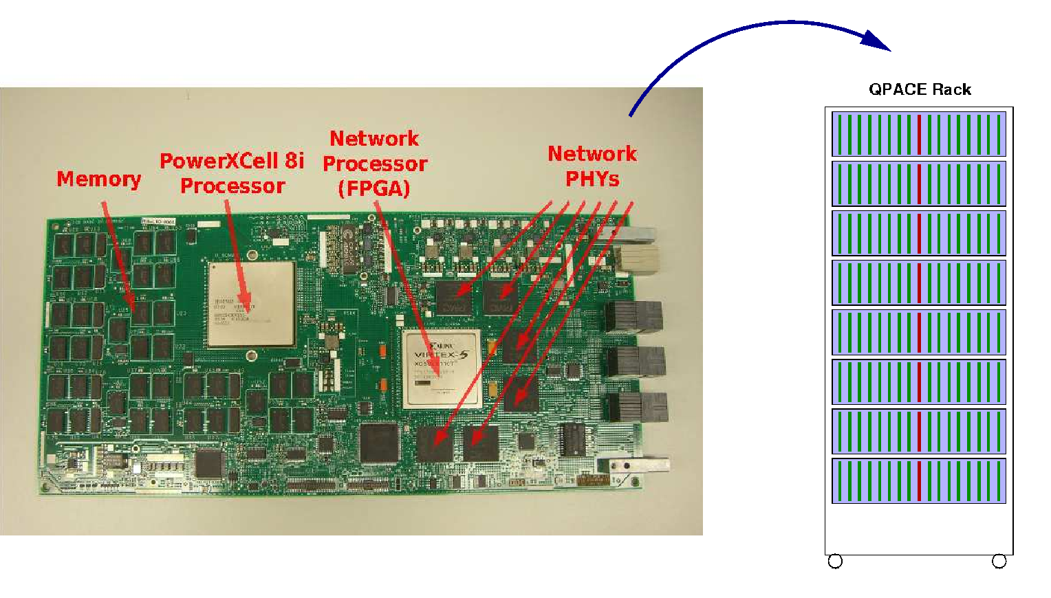
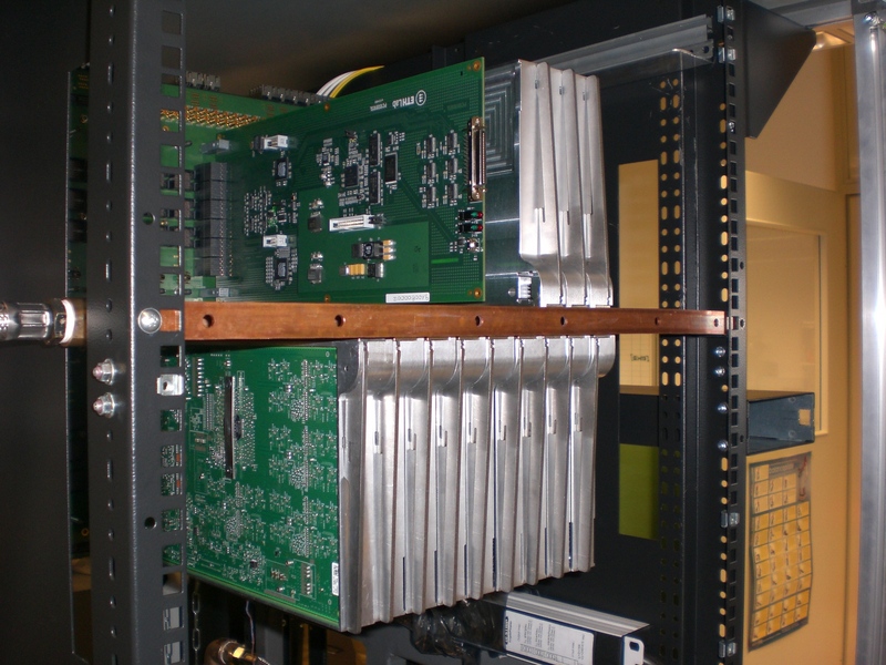
The building block of QPACE is a node card based on IBM’s PowerXCell 8i processor and a Xilinx Virtex-5 FPGA (see Fig. 1, 2). The PowerXCell 8i is the second implementation of the Cell Broadband Engine Architecture [3], very similar to the Cell processor used in the PlayStation 3. The main reason for using this enhanced Cell processor is its support for high-performance double precision operations with IEEE-compliant rounding. The Cell processor contains one PowerPC Processor Element (PPE) and 8 Synergistic Processor Elements (SPE). Each of the SPEs runs a single thread and has its own 256 kBytes on-chip memory (local store, LS) which is accessed by DMA or by local load/store operations from/to 128 general-purpose 128-bit registers. An SPE in the PowerXCell 8i processor executes two instructions per cycle, performing up to 8 single precision (SP) or 4 double precision (DP) floating point (FP) operations. Thus, the total SP (DP) peak performance of all 8 SPEs on a single processor is 204.8 (102.4) GFlops at the nominal clock frequency of 3.2 GHz.
The processor has an on-chip memory controller supporting a memory bandwidth of 25.6 GBytes/s and a configurable I/O interface (Rambus FlexIO) supporting a coherent as well as a non-coherent protocol with a total bidirectional bandwidth of up to 25.6 GBytes/s. Internally, all units of the processor are connected to the coherent Element Interconnect Bus (EIB) by DMA controllers. In QPACE the I/O interface is used to interconnect the PowerXCell 8i processor with the network processor implemented on a Xilinx V5-LX110T FPGA (Fig. 3), using RocketIO transceivers that are able to support the FlexIO physical layer. We plan to use 2 FlexIO links between the multi-core compute processor and the network processor, with an aggregate bandwidth of 6 GBytes/s simultaneously in either direction.
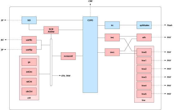
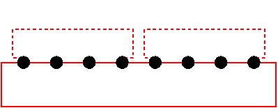
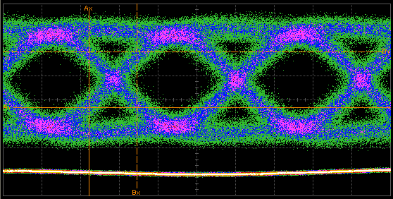
The node cards are interconnected by a three-dimensional torus network with nearest-neighbor communication links. The physical layer of the communication links relies on commercial standards for which well-tested and cheap transceiver hardware components are available. This allows us to move the most timing-critical logics out of the FPGA. Specifically, we use the 10 Gbit/s PMC Sierra PM8358 XAUI transceiver. On top of this standard physical layer we have designed a lean custom protocol optimized for low latencies. Unlike in other existing Cell-based parallel machines, in QPACE we can move data directly from the local store (LS) of any SPE on one node to the LS of any SPE of one of the 6 neighboring nodes. Data do not have to be routed through main memory (to avoid the bottleneck of the memory interface) or the PPE. Rather, data are moved via the EIB directly to or from the I/O interface. The tentative goal is to keep the latency for LS-to-LS copy operations on the order of 1s. 32 node cards are mounted on a single backplane. One dimension of the three-dimensional torus network is completely routed within the backplane. We arrange nodes as one partition of nodes or as multiple smaller partitions. For larger partitions, several backplanes can be interconnected by cables. 8 backplanes sit inside one rack, hosting a total of 256 node cards corresponding to an aggregate peak performance of 26 TFlops (DP). A system with racks can be operated as a single partition with 2 x 16 x 8 nodes.The PMC Sierra PM8358 transceivers have a redundant link interface that we use to repartition the machine (in two of the three dimensions) without the need for recabling. An example of this feature is shown in Fig. 4. The properties of the physical layer of the network have been investigated in detail. Figure 5 displays an example of an eye diagram corresponding to the worst-case situation in a QPACE machine.
On each node card the network processor is also connected to a Gbit-Ethernet transceiver. The Ethernet ports of all node cards connect to standard Ethernet switches housed within the QPACE rack. Depending on the I/O requirements the Ethernet bandwidth between a QPACE rack and a front-end system can be adjusted by changing the bandwidth of the uplinks of the switches.
On each backplane there are 2 root cards which manage and control 16 node cards each (e.g., when booting the machine). The root card hosts a small Freescale MCF5271 Microprocessor operated using uClinux. The microprocessor can be accessed via Ethernet, and from it one can connect to various devices on the node cards via serial links (e.g., UART). The root cards are also part of a global signal tree network. This network sends signals and/or interrupts from any of the node cards to the top of the tree. The combined result result is then propagated to all node cards of a given partition.
Each node card consumes up to 130 Watts. To remove the generated heat a cost-efficient liquid cooling system has been developed, which enables us to reach high packaging densities. The maximum power consumption of one QPACE rack is about 35 kWatts. This translates into a power efficiency of about 1.5 Watts/GFlops (DP, peak).
3 Application software and performance
During an early phase of this project a performance analysis has been done [4] based on models [5] which typically take into account only bandwidth and throughput parameters of the hardware. The overall performance of LQCD applications strongly depends on how efficiently a few computational tasks can be implemented, namely the application of the lattice Dirac operator on a quark field, and various linear algebra operations. For the hopping term of the Wilson-Dirac operator we estimated for realistic hardware parameters a theoretical efficiency of about 30%. The main restrictions come from the performance of the memory interface. While other implementations of the Wilson-Dirac operator code on the Cell processor exist [6, 7], ours is different. We worked out a sophisticated strategy for reading data from memory and storing results back to memory, such that external memory accesses are minimized and a network latency of some s, i.e., O(10,000) clock cycles (at a clock frequency of 3.2 GHz), can be tolerated.
In a real implementation of this application kernel we have verified that on a single processor an efficiency of 25% can be achieved with realistic local lattice sizes for the final machine [8] (see Table 1). The Wilson-Dirac operator and the linear algebra routines (see Tables 2, 3) have been written using SPE intrinsics and sophisticated addressing techniques.
An efficient implementation of applications on the Cell processor is obviously more difficult compared to standard processors. One has to carefully choose the data layout and scheduling of operations in order to optimize utilization of the memory interface. Moreover, the overall performance of the program critically depends on how on-chip parallelization is implemented. To relieve the programmer from the burden of porting efforts we apply two strategies. For a number of kernel routines which are particularly performance-relevant we will provide highly optimized implementations which can be accessed through library calls. To facilitate the implementation of the remaining parts of the code we plan to port or implement software layers that hide the hardware details. The user-level API to manage SPE-to-SPE communications via the torus network will be easy to use with complementary send/receive primitives.
| Lattice | ||
|---|---|---|
| 25% | 24% | |
| 26% | 25% | |
| 26% | 26% | |
| model | 34% | 34% |
| version | caxpy | cdot | rdot | norm 111The difference between benchmark and model is due to limited loop unrolling and sub-optimal instruction scheduling. |
|---|---|---|---|---|
| xlc/asm | 47% | 42% | 38% | 49% |
| model | 50% | 50% | 50% | 100% |
| version | caxpy | cdot | rdot | norm |
|---|---|---|---|---|
| xlc | 3.2% | 5.1% | 2.7% | 5.3% |
| model | 4.1% | 6.2% | 3.1% | 6.2% |
4 Conclusion
QPACE is a next-generation massively parallel computer optimized for LQCD applications. It leverages the power of modern multi-core processors by tightly coupling them within a custom high-bandwidth, low-latency network. The system is not only optimized with respect to procurement costs vs. performance but also in terms of power consumption, i.e., operating costs.
As mentioned above, first prototype hardware is already available. The test of the final hardware configuration is expected to be completed by the end of 2008. In early 2009 we plan to start manufacturing several large machines with an aggregate peak performance of 200 TFlops (DP). The ambitious goal of the project is to make these machines available for research in lattice QCD by mid 2009.
Acknowledgments
QPACE is funded by the Deutsche Forschungsgemeinschaft (DFG) in the framework of SFB/ TR-55 and by IBM. We thank the developers at the IBM lab in La Gaude involved in this project and acknowledge important technical and financial contributions to the project by Eurotech (Italy), Knürr (Germany), and Xilinx (USA).
References
- [1] P.A. Boyle et al., Overview of the QCDSP and QCDOC computers, IBM J. Res. & Dev. 49 (2005) 351
- [2] F. Belletti et al., Computing for LQCD: apeNEXT, Computing in Science & Engineering 8 (2006) 18
- [3] H.P. Hofstee et al., Cell Broadband Engine technology and systems, IBM J. Res. & Dev. 51 (2007) 501
- [4] F. Belletti et al., QCD on the Cell Broadband Engine, PoS (LAT2007) 039
- [5] G. Bilardi et al., The Potential of On-Chip Multiprocessing for QCD Machines, Springer Lecture Notes in Computer Science 3769 (2005) 386
- [6] A. Nakamura, Development of QCD-code on a Cell machine, PoS (LAT2007) 040
- [7] J. Spray, J. Hill, and A. Trew, Performance of a Lattice Quantum Chromodynamics Kernel on the Cell Processor, arXiv:0804.3654 [hep-lat].
- [8] A. Nobile, Performance analysis and optimization of LQCD kernels on the Cell BE processor, PhD Thesis, Univ. Milano-Bicocca, 2008