Superconducting properties of Nb thin films deposited on porous silicon templates
Abstract
Porous silicon, obtained by electrochemical etching, has been used as a substrate for the growth of nanoperforated Nb thin films. The films, deposited by UHV magnetron sputtering on the porous Si substrates, inherited their structure made of holes of 5 or 10 nm diameter and of 10 to 40 nm spacing, which provide an artificial pinning structure. The superconducting properties were investigated by transport measurements performed in the presence of magnetic field for different film thickness and substrates with different interpore spacing. Perpendicular upper critical fields measurements present peculiar features such as a change in the curvature and oscillations in the field dependence of the superconducting resistive transition width at Tesla. This field value is much higher than typical matching fields in perforated superconductors, as a consequence of the small interpore distance.
pacs:
PACS: 74.25.Fy, 74.78.-w, 74.25.Qt, 81.05.RmI Introduction
In order to increase the critical parameters of both low- and high- superconductors, in the last years great efforts were directed towards the optimization of the vortex confinement in these systems. The enhancement of the vortex pinning can be obtained using periodic arrays of different types of artificial defects in superconducting thin films, such as periodic variation of thin film composition Raffy_SSC or heavy ion irradiation Harada . Progress in the fabrication of nanostructures by lithography has given access to a wide variety of well controlled vortex regular pinning arrays at sub-micron length scales Lykov ; Baert ; Morgan . Experiments performed on this kind of samples revealed the presence of peaks in the magnetic field dependence of the critical current density Fiory ; Mosh_size ; Castellanos at matching fields , where is an integer and is the value of the field at which the vortex lattice spacing is equal to the period of the regular array of submicrometer defects, a: . Recently a radically different approach to nanostructures fabrication based on self assembled growth ChemRev , such as chemically anisotropic etching of single crystals, attracted much attention also in the superconducting field. These processes are useful for generating, on large areas, low-cost simple patterns of nanostructures in a single step, assuring a high reproducibility as well. Moreover, these techniques give the opportunity to produce regular periodic structures with features that can be even an order of magnitude smaller than the ones obtained by time consuming e-beam lithography process, leading to templates having features comparable with the characteristic superconducting lengths. In particular, the reduced dimensions are of great importance in the enhancement of the superconducting pinning properties, since smaller interpore spacing implies higher matching fields down to lower temperatures. At this purpose transport and magnetic measurements were already performed on Nb thin films grown on nanoporous Al2O3 templates with pores diameter in the range 25-150 nm Prischepa ; Welp ; Vinckx1 ; Vinckx2 ; Vanacken . Anomalies in the as well as in the temperature dependence of the perpendicular upper critical field were observed.
The aim of this work is to present the superconducting properties of Nb thin films deposited on porous silicon (PS) substrates fabricated by electrochemical etching of monocrystalline Si in an HF solution. Porous silicon is constituted by a network of pores immersed in a nanocrystalline matrix Pavesi . As a result, PS is characterized by a very large chemically reactive internal surface area, which makes this material promising for many technological applications in different fields, as for instance micro and optoelectronics, gas sensing, and biotechnology; recently PS was also applied as a substrate for the nanotubes growth Pavesi ; Jakubowicz . The reason to choose PS as a template for superconducting thin films deposition is twofold. On one hand Si based substrates are good candidates for the Nb growth. Moreover, the characteristic pore features of these PS substrates are the smallest used in superconducting field at this purpose. The porous area of our substrates extends, in fact, on about 1 cm2 and it is constituted by pores of mean diameter, , tunable between 5 and 10 nm, with interpore spacing (the distance between the centers of two nearest pores), , that can be varied from 10 to 40 nm. It is worth to underline that the regularity of the pores arrangement in PS substrates is lower than the one observed in Al2O3 templates obtained by electrochemical oxidation Prischepa2 ; MTemplfi ; Prischepa3 . However it has been recently shown that the interaction of the vortex lattice with templates of artificial pinning centers presenting a short-range order can also give rise to peculiar behavior of both critical magnetic fields and critical currents Eisenmenger . In the same way, thin Nb films deposited on PS substrates can inherit their structure, resulting in porous Nb thin films with in plane geometrical dimensions, and , comparable with the superconducting coherence length, . This reduced periodicity could reflect in peculiar properties of porous thin films, that could be interesting also in view of possible application. For instance tuning the samples geometry (, ) we expect to be able to control the superconducting critical temperature, to reach higher matching fields and eventually also higher critical currents, down to lower temperatures. The superconducting properties of porous Nb thin films have been probed by transport measurements in presence of magnetic fields applied in the direction perpendicular to the samples surface. As a consequence of the high density of the pore network, the (H,T) phase diagrams present a deviation from the classical behavior of , and the behavior shows fingerprints of the periodic anomaly typical of superconducting wire networks. Both these effects appear at fields up to Tesla. This value is larger than typical matching fields of periodic pinning arrays obtained both by lithographic techniques and by using self-organized Al2O3 templates.
II Fabrication and characterization
II.1 Substrates
Porous layers were fabricated by electrochemical anodic etching of p-type, 12 cm, and n-type, 0.01 cm, monocrystalline silicon wafers in 48% water solution of HF at the current density of 25 mA/cm2. n-type silicon wafers were anodized with light exposition by 100 W tungsten lamp as well without light illumination. The anodization time was chosen in the range of 0.5 - 4 min in order to get porous layers with a thickness ranging from 0.5 to 4 m. The integral porosity was estimated by gravimetry to be in the range from 30% up to 60% Lazarouk . For p-type silicon wafers the nominal pore diameter and the interpore spacing are respectively nm and nm. In the case of n-type silicon wafers the nominal pore diameter is nm, while the values of are expected to be 20 nm for light exposed substrates and 40 nm for samples obtained without illumination.
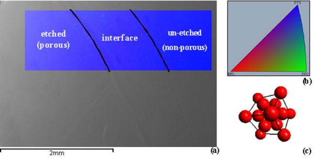
The Electron Back Scatter Diffraction (EBSD) technique has been used to investigate the microstructure of both p-type and n-type porous silicon wafers. EBSD patterns were obtained from LEO EVO 50 Scanning Electron Microscope with an Oxford Inca detector. In order to optimize the contrast in the diffraction pattern and the fraction of electrons scattered from the sample, the substrates were tilted so that an angle of is formed between the normal to the sample surface and the electron beam EBSD . EBSD patterns were acquired on porous and non-porous regions of the two different substrates. Fig. 1 shows crystal orientation map of a 3 mm by 0.5 mm area for a n-type substrate with a spatial resolution of about 80 m2. The scanned area was selected crossing the interface between the etched (porous) and un-etched (non-porous) silicon wafer. The color uniformity of the map reveals that in this area all the crystalline components have (111) orientation. Similarly, the same analysis performed on p-type substrate showed (100) crystallographic orientation on both porous and non-porous region. In both cases the etching process does not influence the crystalline properties of the substrates.
II.2 Nb films
Nb thin films were grown on top of the porous Si substrates in a UHV dc diode magnetron sputtering system with a base pressure in the low mbar regime and sputtering Argon pressure of mbar. Reference films were grown in each deposition run on standard non-porous Si(100) substrates. In order to reduce the possible contamination of the porous templates, the substrates were heated at C for one hour in the UHV chamber. The deposition was then realized at room temperature after the cool off of the system. The films were deposited at typical rates of 0.3 nm/s, controlled by a quartz crystal monitor calibrated by low-angle reflectivity measurements. Since the effect of the periodic template would be reduced when the film thickness, , exceedes the pore diameter, , the Nb thickness was allowed to range between 8.5 and 15 nm. All the samples deposited on porous Si, their names and thicknesses, and the substrate characteristics as well, are summarized in Table 1. For the sake of clarity the samples were named using the initials Si followed by a number indicating the nominal substrate interpore distance, , and by another number for the Nb thickness. For example, Si40-Nb12 is the Nb film 12 nm thick, grown on the porous substrate with nm. The pore diameter is in this case nm.
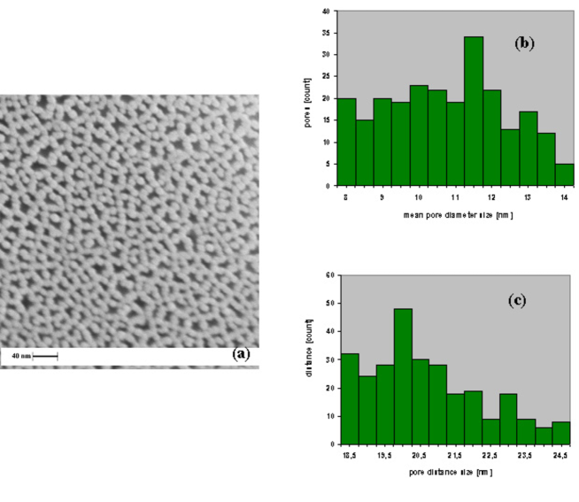
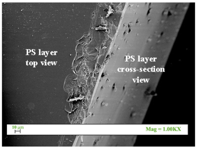
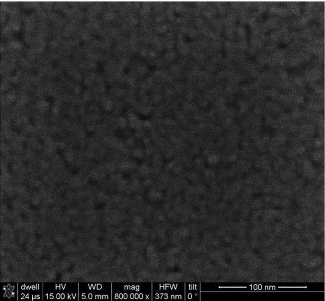
The morphology of the PS substrates as well as of the Nb thin films deposited on them was analyzed by field emission scanning electron microscopy (FESEM). To allow FESEM measurements on highly resistive PS substrates, metallization with 8 nm Pd/Au thin film was realized. A typical FESEM micrograph (magnification = 500000) of the top of the Si20 substrate is shown in Fig. 2(a). At this high magnification the pores can be clearly distinguished as dark areas surrounded by Pd/Au molecular agglomerates. Fig. 2a also reveals that the pore entrances are not regular circles. Several micrographs obtained on PS templates were analyzed in order to evaluate the pore diameter and the interpore spacing distributions resulting from the electrochemical etching. In order to take into account the pores shape we evaluated an “equivalent pore diameter”, defined as the diameter of a circle having the same surface area of the pore. The latter was obtained by the help of ImageTool, a software for image analysis, which enables to supply the surface area of a region drawing a polygon around its outline. The evaluated pore size distribution of the PS layer is reported in Figure 2b (mean diameter nm and standard deviation nm). Moreover, the mean interpore distance nm with a standard deviation of nm (Figure 2c) were estimated. In Fig. 3 a low resolution FESEM image of the Si wafer edge is reported. Along this edge, at about 10 m from the top surface, a change in the morphology can be distinguished, indicating the presence of a porous layer of about 10 m, in agreement with sample specifications. All these values are in very good agreement with the expected nominal ones and indicate the effectiveness of the porogenic treatment. In Fig. 4 a secondary electron FESEM image (magnification = 800000) of a dedicated Nb film, 9 nm thick, deposited on a Si20 substrate is shown. Again, the pores restrict the solid angle from which low energy electrons can escape, thus rendering the pores dark and the top surface light. The surface appearance, far from being perfectly ordered, however clearly reveals the presence of holes in the Nb layer.
III Superconducting properties
The superconducting properties, critical temperatures , and perpendicular upper critical fields as a function of the temperature, , were resistively measured in a 4He cryostat using a standard dc four-probe technique on unstructured samples. was taken at the 50% of the transition curves.
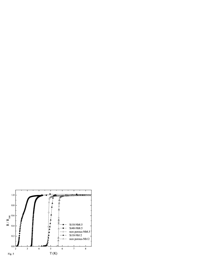
In Fig. 5 are reported the transition curves of Nb thin films of different thickness grown on the porous substrates Si10, namely samples Si10-Nb8.5 and Si10-Nb12, and Si40, namely sample Si40-Nb8.5. It can be observed that the critical temperature, , decreases as the thickness of the Nb film is reduced, as expected Minhaj . The same () dependence is obtained for samples sets deposited on different porous templates. In the same figure the resistive transitions of non-porous reference Nb films are also shown. The critical temperatures of these samples are higher than the of the film with the same thickness deposited on the porous substrates. This difference is less evident for the sample with the larger interpore distance, since the ratio between the non-porous and the porous area is higher in this case so that the critical temperature results less depressed. This reduction could be related, for example, to the highly reactive internal porous surface area Pavesi . From Fig. 5 it also emerges that the difference between porous and non-porous samples is reduced as the Nb thickness is increased due to the fact that, for larger , the pores are mostly covered and their effect on the electronic transport properties is less important. The data show also that the shapes are strongly effected by the pores and the interpore distances dimensions. In fact, while sample Si40-Nb8.5 shows a rather sharp curve, sample Si10-Nb8.5 presents a broad double step transition. This difference, at these reduced Nb thickness and substrate parameters, can be ascribed to the formation of a superconducting wire network made of several thin Nb stripes of different width, and hence to the distribution of transition temperatures for the stripes in the entire sample Pannetier2 ; Wilks ; Zant ; Rammal .
The (H,T) phase diagrams for our samples were obtained performing measurements at fixed magnetic fields and measurements at fixed temperatures. In general, the perpendicular upper critical field of superconducting films of thickness d obeys to a linear temperature dependence,
| (1) |
where is the parallel Ginzburg-Landau coherence length at T = 0. The temperature dependence of is = /. Since the film dimensions in the xy plane are larger than , the expression (1) is verified in the whole temperature range.
Before presenting the results obtained for the Nb films deposited on PS, it is worth to show the curves for two Nb reference films, as reported in Fig. 6. As expected the behavior is linear for both the samples. A fit of the data with the expression (1), yields a value of the Ginzburg-Landau coherence length at T = 0, nm for nm and nm for nm. Thus the pore diameter dimensions in our PS substrates are comparable with the vortex core dimensions at T=0, . This means that each pore can trap only one fluxon, the saturation number being Mkrtchyan . Subsequently multiquanta vortex lattice Mosh_size can not be observed in our systems, which are then suitable for the study of commensurability effect at low temperatures and high magnetic fields.
The curves obtained for the Nb films deposited on porous Si templates present some peculiarities. Fig. 7(a) shows the phase diagram, , of two samples of different thickness grown on the porous Si substrate with nm and nm, namely Si10-Nb8.5 and Si10-Nb12. Similarly, Fig. 7(b) shows dependence of two samples of different thickness grown on the porous Si substrate with nm and nm, namely Si20-Nb12 and Si20-Nb15. In both cases it is clearly visible that the introduction of the porous array modifies the upper critical field behavior of the Nb thin film. is characterized, in fact, by a strong non linear temperature dependence near , which becomes less evident when the Nb thickness exceeds . In the sample Si10-Nb12, where the condition nm nm is realized, the upper critical magnetic field is linear in all the temperature range, as shown by the linear fit in Fig. 7(a). The comparison between two Nb thin films of the same thickness deposited on Si20 and a non-porous substrate is reported in the inset of Fig. 7(b). Apart from a reduction the porous Nb film is again characterized by a non linear dependence. However, for these samples the positive curvature of close to is the only effect we could notice since the extremely small interpore spacing of these two analyzed substrates (Si10, Si20) would produce commensurability effects only at very large magnetic fields, namely 24 and 6 Tesla, respectively. These fields values are not accessible to our experimental set up. On the other hand the matching field should be considerably smaller if Nb films are deposited on a PS substrate with a larger interpore distance. For example, for the porous Si template Si40, Tesla, a reachable value for our experimental set up. For this reason, to study commensurability effects, two films of different thickness were deposited on this substrate, namely samples Si40-Nb8.5 and Si40-Nb12. Moreover, in order to investigate a film with an intermediate Nb thickness, the sample Si40-Nb12 was deliberately oxidized obtaining the formation of about 2 nm thick oxide layer. This sample, with a resulting suppressed superconducting critical temperature, was named Si40-Nb10. The transitions measured for different values of the magnetic fields from 0 to 2 Tesla are presented in the inset of Fig. 8(a) for the sample Si40-Nb10. The resulting (H,T) phase diagram is shown in Fig. 8(a). Similarly, in Fig. 8(b) the dependence is shown for the sample Si40-Nb12. The upper critical fields are again characterized by a non linear temperature dependence near .
Moreover, it is also interesting to note that for these samples the dependencies present first a positive curvature followed by a change in the concavity, which occurs in both cases at Tesla. This effect is more evident if we plot the second derivative versus temperature as shown in Fig. 8(a),(b), right scale. In both cases / shows, in fact, an abrupt change at Tesla, where the anomaly in the dependence is present. Similar features in (H,T) phase diagram were reported for Nb thin films deposited on Al2O3 substrates Prischepa ; Welp ; Vinckx1 , as well as on triangular array produced by micellar technique Eisenmenger . Another peculiarity that can be ascribed to the reduced dimensionality of these samples is observed plotting the transition width, = ( = )( = ), as a function of the field. The dependence, reported in inset of Fig. 8(b) for the sample Si40-Nb12 shows, in fact, a minimum again at Tesla. This feature is in general expected at the matching field, since dissipative effects are reduced as commensurability occurs, resulting in shaper resistive transitions. Both anomalies of the and the behaviors at Tesla, make us confident to identify this field as the first matching field, . Then, it follows that the period of the porous template is a = 48 nm, a value in very good agreement with the nominal interpore spacing of this analyzed sample, nm. The non-monotonic behavior is also reminiscent of the formation of a superconducting wire network. In this case the observed oscillations could be a direct consequence of fluxoid quantization in a multiply connected superconductor, an extension of Little-Parks oscillations of an individual superconducting loops Parks . The expected amplitude of the oscillations can be estimated by the expression Pannetier , which in our case, for a = 48 nm, gives mK, a value close to the one experimentally observed, namely mK.
A fit of the data close to with the expression (1), yields a value of the Ginzburg-Landau coherence length at T = 0, nm and nm, respectively. The values of are significantly smaller than the BCS coherence length of Nb, nm Buckel , indicating that our films are in dirty limit regime with an electron mean free path of l = 1.38 / nm Schmidt . The Ginzburg-Landau parameter, = (0)/, can be estimated using the expression = 0.72/l , where nm is the London penetration depth of Nb Buckel . Ratios of / and (0)/, measured for a = 48 nm, are larger than in previous works Welp ; Vinckx1 on perforated Nb samples, indicating that we are in presence of individual vortex pinning Brandt . Therefore the porous template can overcome the lattice rigidity, being suitable for the vortex lattice pinning in Nb thin films.
IV Conclusions
Critical temperatures and perpendicular upper critical fields measurements were performed on Nb thin films sputtered on different PS substrates obtained by electrochemical etching of Si in a HF solution. The control of the etching parameter allows to obtain templates with pores diameter and interpore distance tunable in the range nm and nm, respectively. These templates were used as a system of pinning arrays in order to obtain the formation of commensurate vortex structures at high matching fields down to low temperatures. Anomalies in the behavior, as well as in the field dependence of the width, were in fact observed at Tesla, which was estimated as the first matching field, . These preliminary results are promising, specially considering that PS prepared by traditional electrochemical etching exhibits a sponge structure, so that the holes are not a regularly distributed ordered planar pinning structure. Future work will focus on critical currents density studies, carried out both by transport measurements on patterned samples and by magnetization measurements. Moreover, due to the extreme reduced features size of PS templates, these systems look appealing also for the studying of two dimensional superconducting wire networks.
S.L. Prischepa gratefully acknowledges the CNR-Italy for financial support within the CNR Short Term Mobility Program.
References
- (1) H. Raffy, E. Guyon, and J.C. Renard, Solid State Commun. 14, 427 (1974).
- (2) T. Matsuda, K. Harada, H. Kasai, O. Kamimura, and A. Tonomura, Science 271, 1393 (1996).
- (3) A.N. Lykov, Solid St. Commun. 86, 531 (1993).
- (4) M. Baert, V.V. Metlushko, R. Jonckheere, V.V. Moshchalkov, and Y. Bruynseraede, Phys. Rev. Lett. 74, 3269 (1995).
- (5) David J. Morgan and J.B. Ketterson, Phys. Rev. Lett. 80, 3614 (1998).
- (6) A.T. Fiory, A.F. Hebard, and S. Somekh, Appl. Phys. Lett. 32, 73 (1978).
- (7) V.V. Moshchalkov, M. Baert, V.V. Metlushko, E. Rosseel, M.J. Van Bael, K. Temst, and Y. Bruynseraede, Phys. Rev. B 57, 3615 (1998); and references therein.
- (8) A. Castellanos, R. Wördenweber, G. Ockenfuss, A. v.d. Hart, and K. Keck, Appl. Phys. Lett. 71, 962 (1997).
- (9) Y. Xia, J.A. Rogers, K.E. Paul, and G.M. Whitesides, Chem. Rev. 99, 1823 (1999).
- (10) S.L. Prischepa, L.M. Lynkov, A.N. Lykov, and V.I. Dedyu, Cryogenics 34, 851 (1994).
- (11) U. Welp, Z.L. Xiao, J.S. Jiang, V.K. Vlasko-Vlasov, S.D. Bader, G.W. Crabtree, J. Liang, H. Chik, and J.M. Xu, Phys. Rev. B 66, 212507 (2002).
- (12) W. Vinckx, J. Vanacken, V.V. Moshchalkov, S. Mátéfi-Tempfli, M. Mátéfi-Tempfli, S. Michotte, and L. Piraux, Eur. Phys. J. B 53, 199 (2006).
- (13) W. Vinckx, J. Vanacken, V.V. Moshchalkov, S. Mátéfi-Tempfli, M. Mátéfi-Tempfli, S. Michotte, L. Piraux, and X. Ye, Physica C 459, 5 (2007).
- (14) J. Vanacken, W. Vinckx, V.V. Moshchalkov, S. Mátéfi-Tempfli, M. Mátéfi-Tempfli, S. Michotte, L. Piraux, and X. Ye, Physica C (2008), doi:10.1016/j.physc.2007.11.070.
- (15) O. Bisi, S. Ossicini, and L. Pavesi, Surf. Sci. Rep. 38, 1 (2000).
- (16) J. Jakubowicz, Superlattice Microst. 41, 205 (2007).
- (17) L.M. Lynkov, S.L. Prischepa, and L.V. Semenyakov, Doklady of Belarus Academy of Sciences 34, 238 (1990), (in Russian).
- (18) S. Mátéfi-Tempfli, M. Mátéfi-Tempfli, and L. Piraux, Thin Solid Films 516, 3735 (2008).
- (19) V.I. Dediu, A.N. Lykov, S.L. Prischepa, L.M. Lynkov, L.V. Semenyakov, V.A. Samokhval, and S.A. Kostuchenko, Preprint 27, 39 (1988), Moscow, FIAN, (in Russian).
- (20) J. Eisenmenger, M. Oettinger, C. Pfahler, A. Plettl, P. Walther, and P. Ziemann, Phys. Rev. B 75, 144514 (2007).
- (21) S.K. Lazarouk, A.V. Dolbik, V.A. Labunov, and V.E. Borisenko in Physics, Chemistry and Application of Nanostructures, World Scientific 223, (2007).
- (22) A.J. Schwartz, M. Kumar, and B.L. Adams, Electron Backscatter Diffraction in Materials Science, (Kluwer Academic, New York, 2000).
- (23) M.S.M. Minhaj, S. Meepagala, J.T. Chen, and L.E. Wenger, Phys. Rev. B 49, 15235 (1994).
- (24) B. Pannetier, J. Chaussy, R. Rammal, and J.C. Villegier, Phys. Rev. Lett. 53, 1845 (1984).
- (25) Carlos W. Wilks, Rick Bojko, and Paul M. Chaikin, Phys. Rev. B 43, 2721 (1991).
- (26) H.S.J. van der Zant, M.N. Webster, J. Romijn, and J.E. Mooij, Phys. Rev. B 50, 340 (1994).
- (27) R. Rammal, T.C. Lubensky, and G. Toulouse, Phys. Rev. B 27, 2820 (1983).
- (28) G.S. Mkrtchyan and V.V. Shmidt, Zh. Eksp. Teor. Fiz. 61, 367 (1971) [Sov. Phys. JETP 34, 195 (1972)].
- (29) R.D. Parks and W.A. Little, Phys. Rev. A 133, 97 (1964).
- (30) A. Bezryadin and B. Pannetier, J. Low Temp. Phys. 98, 251 (1995).
- (31) W. Buckel, Supraleitung, 3rd edn. (Physik-Verlag, Weinheim, 1984).
- (32) V.V. Schmidt, The Physics of Superconductors, (Springer, Berlin-Heidelberg, 1997).
- (33) H. Brandt, Phys. Lett. 77A, 484 (1980).
| Sample | (nm) | (nm) | (nm) | (K) |
|---|---|---|---|---|
| Si10-Nb8.5 | 51 | 102 | 8.5 | 2.48 |
| Si10-Nb12 | 51 | 102 | 12 | 4.68 |
| Si20-Nb12 | 102 | 204 | 12 | 4.06 |
| Si20-Nb15 | 102 | 204 | 15 | 6.18 |
| Si40-Nb8.5 | 102 | 406 | 8.5 | 3.49 |
| Si40-Nb10 | 102 | 406 | 10 | 5.17 |
| Si40-Nb12 | 102 | 406 | 12 | 5.94 |


![[Uncaptioned image]](/html/0810.1447/assets/x9.png)
![[Uncaptioned image]](/html/0810.1447/assets/x10.png)