On the Zero-Bias Anomaly in Quantum Wires
Abstract
Undoped GaAs/AlGaAs heterostructures have been used to fabricate quantum wires in which the average impurity separation is greater than the device size. We compare the behavior of the Zero-Bias Anomaly against predictions from Kondo and spin polarization models. Both theories display shortcomings, the most dramatic of which are the linear electron-density dependence of the Zero-Bias Anomaly spin-splitting at fixed magnetic field and the suppression of the Zeeman effect at pinch-off.
pacs:
72.10.Fk, 72.25.Dc, 73.21.Hb, 73.23.AdSplit gates Thornton et al. (1986) can be used to restrict transport from a two-dimensional electron gas (2DEG) to a ballistic one-dimensional (1D) channel. This results in the quantization of the differential conductance in units of at zero magnetic field van Wees et al. (1988); Wharam et al. (1988). A shoulder on the riser of the first quantized plateau, the “0.7 anomaly” or “0.7 structure” Thomas et al. (1996), is not completely understood but generally acknowledged to result from electron-electron interactions. Although spin polarization models Wang and Berggren (1996); Kristensen et al. (2000); Reilly et al. (2002); Graham et al. (2007); Sfigakis et al. (2008a); Berggren and Yakimenko (2008) and 1D Kondo physics models Cronenwett et al. (2002); Meir et al. (2002); Rejec and Meir (2006) can describe many experiments, neither can explain all phenomena associated with the 0.7 structure. One example is the so-called zero-bias anomaly (ZBA): a peak in centered at for when sweeping source-drain bias at a fixed gate voltage at low temperature . Spin polarization models cannot alone predict its occurrence in quantum wires, although an embedded impurity near or in the 1D channel could produce a ZBA via the 0D Kondo effect Meir et al. (1993); Goldhaber-Gordon et al. (1998); Cronenwett et al. (1998); van der Wiel et al. (2000). On the other hand, in 1D Kondo physics models, a bound state forms when . In this context, a resonance observed by a non-invasive detector capacitively coupled to a quantum wire at threshold Yoon et al. (2007) as well as a triple-peaked structure in at fixed below the 0.7 structure Sfigakis et al. (2008b) are consistent with the presence of a localized state in 1D channels.
Systematically studying the ZBA in modulation-doped 2DEGs has proven difficult because of the large variability of its characteristics from device to device Graham et al. (2008); Griffiths (unpublished), probably due to the randomly fluctuating background potential caused by the ionized dopants, significant even with the use of large (75 nm) spacer layers. This disorder is so pervasive that one can be led to wonder whether the ZBA always results from interactions between conduction electrons and a random localized state near the 1D channel. However, disorder can be dramatically reduced in undoped GaAs/AlGaAs heterostructures where an external electric field (via a voltage on a metal top gate) electrostatically induces the 2DEG Harrell et al. (1999); Sarkozy et al. (2008). Figure 1(a) shows the advantages of this technique, particularly at low carrier densities (see also Fig. 3 in Ref. Harrell et al. (1999)), a regime most relevant for the ZBA.
In this Letter, we report on the study of the ZBA in ten quantum wires fabricated in undoped GaAs/AlGaAs heterostructures. We demonstrate that an unsplit ZBA does not result from interactions between conduction electrons and a random localized state near the 1D channel: it is a fundamental property of 1D channels, in disagreement with spin polarization models. Another inconsistency is a suppression of the Zeeman effect at pinch-off. In disagreement with Kondo theory, we observe a non-monotonic increase of the Kondo temperature with , and a linear peak-splitting of the ZBA with at a fixed .
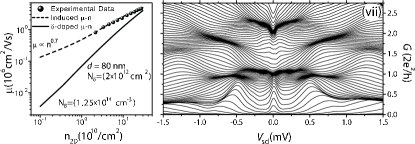
The two wafers primarily used in this study, T622 (T623) with a 317 (117) nm deep 2DEG, were grown by molecular beam epitaxy and consisted of: a 17 nm GaAs cap, 300 (100) nm of Al.33Ga.67As/GaAs, 1 m of GaAs, and a 1 m superlattice with a 5 nm Al.33Ga.67As/5 nm GaAs period. No layer was intentionally doped. For T622, cm-2. Figure 1(a) shows the mobility versus the 2D sheet carrier density for T622; wafer T623 has slightly higher mobilities, e.g. 1.7 cm2/Vs versus 1.6 cm2/Vs at 51010 cm-2. Using Matthiessen’s rule far from the localization regime, the experimental data is fit to standard models of scattering times Ando et al. (1982); Gold (1988). The dominant sources of scattering in our system (analyzed in Ref. Sarkozy et al. (2008)) are charged background impurities and interface roughness, from which we extracted the background impurity concentration cm-3. Intersecting the background impurity potential with a 2DEG wavefunction of width nm yields a minimum average distance between scattering centers m in wafer T622. A similar number is found for wafer T623.
Ten quantum wires, labeled (i)–(x) throughout this paper (seven from T622 and three from T623), were measured in two dilution refrigerators (with base electron temperature 60 mK and 150 mK), using standard lock-in techniques and varying , , , and . Following a mesa etch, recessed ohmic contacts (Ni/AuGe/Ni/Ti/Pt) were deposited and annealed Sarkozy et al (2007). A voltage can be applied to surface Ti/Au split gates of length nm with width nm on on T622 (T623). Polyimide insulated the inducing Ti/Au top gate from other gates and ohmic contacts.
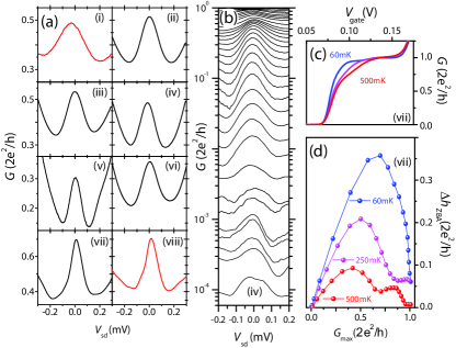
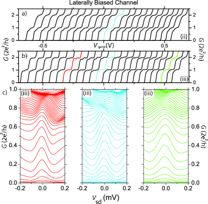
Although the average distance between impurities is m, their distribution is not uniform. In analogy to mean-free-path calculations, the probability of finding an impurity within a 1D channel of length is 50%. For , an unsplit, symmetric ZBA was observed in all ten devices. Figure 2(a) shows the ZBA in eight of these. It is thus unlikely (of order ) that all such occurrences were the result of interactions between conduction electrons and some localized state near the 1D channel.
Defining as the maximum conductance achieved at base , , and for each value of , Fig. 2(b) shows that increases monotonically with (as in all our devices). Defining as minus the average conductance of the local minima on the rhs and lhs of the ZBA, Fig. 2(d) shows that decreases as increases for all , as would be expected from Kondo physics. As increases, a local minimum near becomes more pronounced. In a previous study on doped quantum wires (see Fig. 6 in Ref. Sfigakis et al. (2008b)), similar plots of also showed a local minimum near . Figure 2(c) links its appearance to the formation of the 0.7 structure.
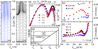
Varying affects the Fermi energy of electrons entering the 1D channel from the 2D leads, as well as the 1D confinement potential [e.g. increasing V in Fig. 3(a) to V in Fig. 3(b), the energy-level spacing between the first two 1D subbands increases from 0.6 to 0.8 meV]. Figure 3(c) shows no clear trend for with increasing , but the minimum near remains present in all curves. In the Kondo formalism [Fig. 3(d)], a specific is associated with each , and the full width at half maximum (fwhm) of the ZBA should scale linearly either with its if , or with if Glazman and Raikh (1988); Cronenwett et al. (1998). For in Fig. 3(f), we do not use the fwhm as it is difficult to distinguish the ZBA unambiguously from the bell-shape traces of just below a plateau (see Fig. 6 in Ref. Martin-Moreno et al. (1992)). For at V, the fwhm remain essentially flat: . For , increasing appears to increase beyond mK. An upper limit of at each can be estimated van der Wiel et al. (2000). In most devices, regardless of whether the 0.7 structure is visible or not, the fwhm has a local minimum near . Identical minima are also observed in doped GaAs quantum wires (see Fig. 3 in Ref. Cronenwett et al. (2002)) and in GaN quantum wires (see Fig. 4 in Ref. Chou et al. (2005)). Near , we interpret the fwhm minimum to indicate a suppression of Kondo interactions, leading to a non-monotonic increase of from pinch-off to , in direct contradiction to 1D Kondo theory Meir et al. (2002). Kondo theory also predicts that fwhm() will increase more than fwhm() as increases [i.e. in Fig. 3(d)]. However, in further disagreement with theory, Fig. 3(e) shows the opposite behavior: the fwhms associated with the larger Kondo temperatures increase the most.
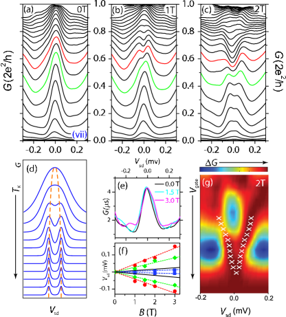
Figures 4(a)–(c) show how the ZBA spin-splits at low . At a fixed , the peak-to-peak separation increases almost linearly with [Fig. 4(g)]. In an in-plane , pinch-off voltage can change due to diamagnetic shift Stern (1968), making an unreliable marker. However, is mostly insensitive to , while the ZBA changes significantly. Thus, fitting the linear relation to the red points in Fig. 4(f), obtained from all red traces with at mV in Figs. 4(a)–(c), yields V/T. For all green traces with at mV in Figs. 4(a)–(c), Fig. 4(f) yields V/T. As decreases [from the red traces in Figs. 4(a)–(c) down to pinch-off], appears to continuously decrease from 86 V/T to small values [e.g. V/T from peak-fitting two asymmetric gaussians to Fig. 4(e)].
At finite , the ZBA in quantum dots splits into two peaks Cronenwett et al. (1998), whose peak-to-peak separation is a defining characteristic of the Kondo effect Meir et al. (1993) where is the Bohr magneton and the effective Landé factor. Figure 4(d) illustrates three distinct regimes one would expect from the singlet Kondo effect at fixed and Pustilnik and Glazman (2004); Potok et al. (2007). In the topmost traces, : spin-splitting cannot be resolved. In the middle traces, : the linewidth of each split peak is narrow enough to make the splitting visible. In the bottom traces, : the split peaks shrink but their splitting should remain constant as long they are still resolvable. However, in our quantum wires, this is clearly not the case. The variation of with in Fig. 4(b)–(c) cannot be reconciled with singlet Kondo physics.
In quantum dots, the ZBA splitting can vary with for (Fig. 4 in Ref. Jeong et al. (2001), Fig. 3 in Ref. Chen et al. (2004)) from the competition between the Kondo effect and the Ruderman-Kittel-Kasuya-Yosida (RKKY) interaction between two localized spins Dias da Silva et al. (2006). Although two such localised spins are predicted to form in quantum wires near pinch-off Rejec and Meir (2006); Berggren and Yakimenko (2008) and these could explain the behavior observed in Figs. 4(b)–(c), this scenario would also require the ZBA to be split at . This is not the case [Figs. 2(b), 3(a)–(b), 4(a), 5(c)]: the two-impurity Kondo model is not applicable.
In spin-polarization models Wang and Berggren (1996); Kristensen et al. (2000); Reilly et al. (2002); Graham et al. (2007); Sfigakis et al. (2008a); Berggren and Yakimenko (2008), the energy difference between spin-up and spin-down electrons includes , an exchange-enhanced spin splitting that could account for previous observations of an enhanced factor above the value of bulk GaAs Thomas et al. (1996). Neglecting correlation effects, the bare exchange energy in 1D scales linearly with . Assuming , the almost linear splitting of the ZBA is consistent with a density-dependent spin polarization. However, this scenario would also require that the minimum value of be the bare Zeeman energy eV/T. This is not what we observe: eV/T in Fig. 4(e). Instead, we find , where [Fig. 4(f)]. The Zeeman effect can be suppressed () if a 2DEG significantly penetrates into the AlGaAs barriers Kogan et al. (2004), at high or if the 2DEG is close to the surface. Neither situation applies to our devices. The suppression of the bare Zeeman effect at pinch-off in our quantum wires is not consistent with spin polarization models.
Despite their exceptional device-to-device reproducibility (compared with doped wires), undoped quantum wires are not free from disorder [Fig. 5(b)]. The apparent splitting for in some of our devices [Fig. 5(c)] is not due to spontaneous spin-splitting or RKKY vs. Kondo interactions, but rather to resonant backscattering or length resonances Lindelof and Aagesen (2008). By increasing the 2D density (and thus long-range screening), many disorder-related effects can be minimized.
In summary, we provide compelling evidence for the ZBA to be a fundamental property of quantum wires. Its continued presence from down to suggests it is a different phenomenon to the 0.7 structure, as proposed in Yoon et al. (2007); Sfigakis et al. (2008b). Both 1D Kondo physics and spin polarization models fall short of accurately predicting experimental observations. For 1D Kondo physics models, these are: (i) a non-monotonic increase of with , (ii) the fwhm of the ZBA not scaling with max[] as increases, and (iii) a linear peak-splitting of the ZBA with at fixed . Spin polarization models can account neither for the occurrence of the ZBA nor for the suppression of the bare Zeeman effect at pinch-off. It is hoped that further refinements in theory will account for these observations.
The authors acknowledge D. Anderson, H. Quach and C. Namba for electron beam patterning, and V. Tripathi, K.-F. Berggren, A.R. Hamilton, C.J.B. Ford, J.P. Griffiths, T.M. Chen, K.J. Thomas, and N.R. Cooper for useful discussions. S. Sarkozy acknowledges financial support as a Northrop Grumman Space Technology Doctoral Fellow. I. Farrer thanks Toshiba Research Europe for financial support.
References
- Thornton et al. (1986) T. J. Thornton, M. Pepper, H. Ahmed, D. Andrews, and G. J. Davies, Phys. Rev. Lett. 56, 1198 (1986).
- van Wees et al. (1988) B. J. van Wees et al., Phys. Rev. Lett. 60, 848 (1988).
- Wharam et al. (1988) D. A. Wharam et al., J. Phys. C 21, L209 (1988).
- Thomas et al. (1996) K. J. Thomas et al., Phys. Rev. Lett. 77, 135 (1996).
- Wang and Berggren (1996) C. K. Wang and K. F. Berggren, Phys. Rev. B 54, R14257 (1996).
- Kristensen et al. (2000) A. Kristensen et al., Phys. Rev. B 62, 10950 (2000).
- Reilly et al. (2002) D. J. Reilly et al., Phys. Rev. Lett. 89, 246801 (2002).
- Graham et al. (2007) A. C. Graham, D. L. Sawkey, M. Pepper, M. Y. Simmons, and D. A. Ritchie, Phys. Rev. B 75, 035331 (2007).
- Sfigakis et al. (2008a) F. Sfigakis et al., J. Phys.: Condens. Matter 20, 164213 (2008a).
- Berggren and Yakimenko (2008) K. F. Berggren and I. Yakimenko, J. Phys.: Condens. Matter 20, 164203 (2008).
- Cronenwett et al. (2002) S. Cronenwett et al., Phys. Rev. Lett. 88, 226805 (2002).
- Meir et al. (2002) Y. Meir, K. Hirose, and N. S. Wingreen, Phys. Rev. Lett. 89, 196802 (2002).
- Rejec and Meir (2006) T. Rejec and Y. Meir, Nature 442, 900 (2006).
- Meir et al. (1993) Y. Meir, N. S. Wingreen, and P. A. Lee, Phys. Rev. Lett. 70, 2601 (1993).
- Goldhaber-Gordon et al. (1998) D. Goldhaber-Gordon et al., Nature 391, 156 (1998).
- Cronenwett et al. (1998) S. M. Cronenwett et al., Science 281, 540 (1998).
- van der Wiel et al. (2000) W. G. van der Wiel et al., Science 289, 2105 (2000).
- Yoon et al. (2007) Y. Yoon et al., Phys. Rev. Lett. 99, 136805 (2007).
- Sfigakis et al. (2008b) F. Sfigakis et al., Phys. Rev. Lett. 100, 026807 (2008b).
- Graham et al. (2008) A. C. Graham et al., submitted to Phys. Rev. B (2008).
- Griffiths (unpublished) J. P. Griffiths (unpublished).
- Harrell et al. (1999) R. H. Harrell et al., Appl. Phys. Lett. 74, 2328 (1999).
- Sarkozy et al. (2008) S. Sarkozy et al., submitted to Appl. Phys. Lett. (2008).
- Ando et al. (1982) T. Ando, A. B. Fowler, and F. Stern, Rev. Mod. Phys. 54, 437 (1982).
- Gold (1988) A. Gold, Phys. Rev. B 38, 10798 (1988).
- Sarkozy et al (2007) S. Sarkozy et al, Electrochemical Soc Proc. 11, 75 (2007).
- Glazman and Raikh (1988) L. Glazman and M. Raikh, JETP Letters 47, 452 (1988).
- Martin-Moreno et al. (1992) L. Martin-Moreno, J. T. Nicholls, N. K. Patel, and M. Pepper, J. Phys.: Condens. Matter 4, 1323 (1992).
- Chou et al. (2005) H. T. Chou et al., Appl. Phys. Lett. 86, 073108 (2005).
- Stern (1968) F. Stern, Phys. Rev. Lett. 21, 1687 (1968).
- Pustilnik and Glazman (2004) M. Pustilnik and L. I. Glazman, J. Phys.: Condens. Matter 16, R513 (2004).
- Potok et al. (2007) R. M. Potok et al., Nature 446, 167 (2007).
- Jeong et al. (2001) H. Jeong, A. M. Chang, and M. R. Melloch, Science 293, 2221 (2001).
- Chen et al. (2004) J. C. Chen, A. M. Chang, and M. R. Melloch, Phys. Rev. Lett. 92, 176801 (2004).
- Dias da Silva et al. (2006) L. G. G. V. Dias da Silva, N. P. Sandler, K. Ingersent, and S. E. Ulloa, Phys. Rev. Lett. 97, 096603 (2006).
- Kogan et al. (2004) A. Kogan et al., Phys. Rev. Lett. 93, 166602 (2004).
- Lindelof and Aagesen (2008) P. E. Lindelof and M. Aagesen, J. Phys.: Condens. Matter 20, 164207 (2008).