Coherent electronic transport through graphene constrictions:
sub-wavelength regime and optical analogies
Abstract
Graphene two-dimensional nature combined with today lithography allows to achieve nanoelectronics devices smaller than the Dirac electrons wavelength. Here we show that in these graphene subwavelength nanodevices the electronic quantum transport properties present deep analogies with classical phenomena of subwavelength optics. By introducing the concept of electronic diffraction barrier to represent the effect of constrictions, we can easily describe the rich transport physics in a wealth of nanodevices: from Bethe and Kirchhoff diffraction in graphene slits, to Fabry-Perot interference oscillations in nanoribbons. The same concept applies to graphene quantum dots and gives new insigth into recent experiments Geim on these systems.
pacs:
72.10.-d, 72.10.Fk, 42.25.-p, 42.25.FxAnalogies play a preminent role in physics. They allow the transfer of notions and concepts from one field to another, thus leading to deeper insights and advances in both fields. In particular, attempts to explore an analogy between the fields of quantum transport and optics have been suggested in the past, both in the direction of optics, for instance in order to understand coherent multiple scattering of light Wolf , and also in the reverse direction Datta . Optical concepts have also been exploited to explain different properties in graphene Altshuler . In this work we develop the analogy between quantum transport and optics beyond those attempts and bridge coherent electronic transport with sub-wavelength optics. Indeed graphene Novoselov ; Kim ; Berger , either in the exfoliated or in the epitaxial form, has extraordinary coherence properties. The electron mean free-path can be of the order of a micron at room temperature and the Dirac electrons wavelength can be up to 100 nm or even larger A . From a technological point of view, graphene can be manipulated by ordinary lithography to realize devices as small as few nanometers B thus achieving a sub-wavelength regime. This suggests that an analogy with sub-wavelength optics can reveal fruitful in order to have a better insight into graphene transport properties. We believe that this approach could ease the task to find a solution to the formidable quantum transport problem of calculating the conductance characteristics in nanodevices.
We will show that, by introducing the hybrid “electronics-optics” concept of electronic diffraction barrier to represent constrictions at contacts, we can describe in an easy way the rich transport physics in a wealth of sub-wavelength graphene nanodevices: from the simplest systems such as slits between two half graphene planes, to graphene nanoribbons or quantum dots sandwiched in between semi-infinite graphene sheets as leads Bethe ; Ebbesen ; Ozbay ; Barnes ; Cavity2 ; Takakura ; Suckling . Our methodology relies on an exact numerical calculation of the conductance within a tight-binding Wallace and a Landauer quantum transport formalisms Datta . The novelty here introduced is that the Landauer equation is solved via a new recursive numerical algorithm MayouRecursion .
Our results give new insights on the conductance characteristics of experimentally synthetized graphene quantum dots Geim ; Ensslin where a chaotic Dirac billiard behaviour has been recently observed Geim . The diffraction barrier concept explains electron localization and allows us to provide a new interpretation of experimentally observed features observed into this system as due to diffraction phenomena occurring at the divergent wavelength of electrons at the Dirac point. We believe that the analogy can be further pushed to play a fruitful and key role in the design of new graphene nanodevices exhibiting other original and interesting characteristics. We also point out that the present findings are not only specific of graphene Dirac electrons but could be extended to other sub-wavelength devices made by 2D electron gas such as GaAs/AlAs or in molecular electronics.
Conductance of graphene slits and diffraction by an aperture – The archetype experiment showing an optical diffraction behaviour is the transmission through a slit or hole. We considered slits made into a graphene sheet (Fig. 1) 111Here the edges of the graphene half-planes are taken of the armchair type. and calculated the conductance. We took into account several slits differing by the width , from the thinnest consisting only of a single motif, i.e. a single hexagon. We introduce the wavelength of the incident Dirac electrons, related to the channel energy via where is the Dirac electrons wavevector, is the energy, linearly dispersed in graphene with a Fermi velocity of ms-1 Kim .
In Fig. 1 we report the conductance of the slits as a function of . We first remark (Fig. 1 inset) an universal scaling behaviour independent of the slit width and depending only on the ratio . This scaling breaks down when the wavelength is nm, that is the energy is eV. Indeed, as shown below, this scaling is intimately related to the scaling properties of the Dirac equation which in graphene is valid only in the low energy or long wavelength limit.
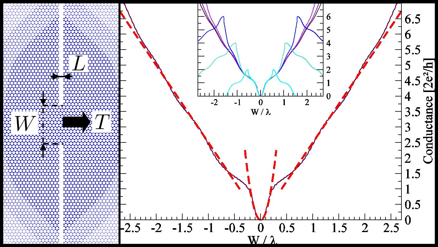
We then notice that in the limit , the conductance is quadratic, with the conductance , while in the opposite limit , the conductance turns out to be linear with . The crossover between the two regimes occurs around . This promptly reminds of an analogy with classical optics and hence offers an immediate interpretation: the conductance response of a graphene slit is a clear manifestation of a diffraction phenomenon. Indeed we can identify two different diffraction regimes: for wavelengths , much larger than the aperture, we observe a Bethe-like diffraction regime Bethe with a slit transmitted energy proportional to the square of the aperture. On the other hand, for one has a Kirchhoff-like diffraction regime, the transmitted energy being proportional to the aperture. Note that weak-localization effects in quantum billards can also reveal diffraction effects in the Kirchoff regime at the lead mouth Ludger . In the short wavelength regime the phenomenon of diffraction is a perturbation and a semi-classical description of the electrons as ballistic wavepackets is applicable, thus leading to a transmitted current proportional to the section of the slit . By contrast, in the subwavelength regime the transmission is lower than given by the semi-classical picture and can be viewed as a tuneling process.
In the ordinary optical diffraction of the slit transmitted intensity, an universal scaling behaviour is observed due to the scaling invariance of Maxwell equations. Here it stems from the fundamental scaling invariance of the graphene 2D Dirac equation. Indeed if a spinor satisfies the Dirac equation for the energy and wavelength then the spinor satisfies the Dirac equation for the energy and wavelength . This leads to the fact that the conductance undergoes a scale invariance . As a consequence the conductance only depends on a reduced argument , . 222The argument is as follows. Let us consider a system where each half plane of graphene is replaced by a ribbon of width . The symmetry axis of the ribbon is perpendicular to the slit, passing by the center of the slit. The conductance for half graphene plane is . We consider a continuous type model of graphene circuit Footnote2 . In this model the mass term of the Dirac equation is zero in the graphene zone and infinite outside. This confines the electrons in the graphene zone. Then there is a one to one correspondence between the scattering states at wavelength ribbon width , slit width and those at wavelength , ribbon width and slit width . This means that the conductance satisfies and as a consequence . Let us note that a scaling relation can also exist for other geometries. In that case the conductance of the circuit will depend only on the ratio between the characteristic lengthes of the circuit and the wavelength .
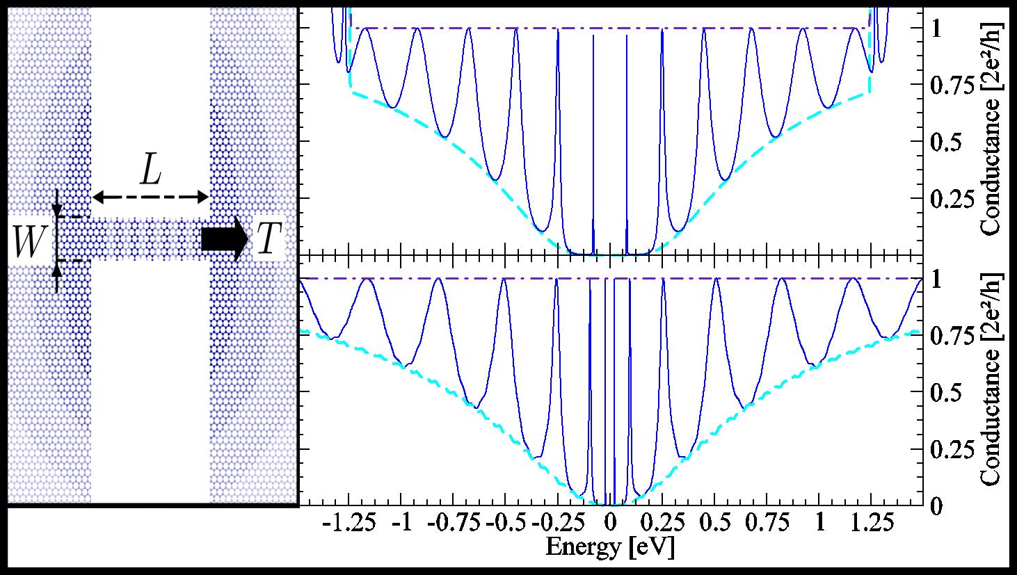
Nanoribbons as Fabry-Perot interferometers and subwavelength waveguides – Here we study the quantum transport response of finite-length metallic graphene nanoribbons and show that they present an oscillating response, typical of optical interferometers, and behave as subwavelength waveguides. We consider two ribbons, a zigzag and an armchair both chosen with a metallic character and hence an available conductance channel at the Dirac energy dresselhaus . The geometry is presented in Fig. 2 and we have taken a length of nm for the armchair nanoribbon and nm for the zigzag (see Fig. 3 for the detailed geometry of each junction). The calculated conductance for both ribbons is shown in Fig. 2 where we again observe a conductance going to 0 at the Dirac point. However in this case, the most evident features are large amplitude oscillations in the conductance, from maxima values of 1 to minima disposed along an envelope function. These systems behave as Fabry-Perot cavities, exactly as in subwavelength optical metallic waveguides Cavity2 ; Takakura ; Suckling . To demonstrate this we show that the nanoribbons calculated oscillating conductance distributes like the Fabry-Perot standard transmittance which is the Airy function:
| (1) |
where is the phase difference after one loop in the nanoribbon. is the wavevector of the Bloch state in the infinite ribbon with energy . is the phase factor acquired at each reflection. is the length of the Fabry-Perot interferometer. is the finesse coefficient and is the reflection coefficient at each end of the nanoribbon, that is at the junction.
The Airy function presents maxima equal to 1 when is an integer multiple of . For sufficiently large the phase varies rapidly with energy, as compared to ; and the minima occur essentially when is maximum, that is at , and envelope along the function
| (2) |
which is independent of the length of the ribbon. We indeed checked that the envelope functions of the conductance minima, as expected from Eq. (2), is independent of the ribbon length. In particular the minimum of the transmission tends to zero at the Dirac energy, which indicates that tends to at zero energy.
Another feature of the Fabry-Perot resonnances concerns their width. The peaks full width at half maximum is where and is the group velocity at energy . The velocity is bounded, such as the peaks look thin when is close to 1, and broaden when . In our case when the peaks seem to have negligible width, indicating again that , and broaden for the higher energies, indicating lower values of .
The relative variation of the conductance (i.e. the ratio between the maximum and minimum conductance between two peaks) is also maximum close to the Dirac energy, due to the nearly perfect confinement at this energy (). We consider in the following that resonances are well defined if the maximum to minimum ratio is greater than . In our calculations this corresponds to a criterion where is the width of the nanoribbon.
The concept of electronic diffraction barrier at a constriction – Fabry-Perot oscillations occur due to the reflection at the junctions/ends of the nanoribbons. We now analyse this reflection and the response of the elementary junction. We consider the same metallic zigzag and armchair ribbons as before, but take them as semi-infinite (Fig. 3). If the system were ballistic (infinite ribbon, no contact resistance and no reflexion), we would expect to observe a conductance equal to 1 quantum of conductance () (dot-dashed line in Fig. 3) in the range of the Dirac energy. Instead, the calculated transmittance through the junction (continous line in Fig. 3) is observed to drop to zero at the Dirac energy, no matter the chirality, exactly like in slits and the nanoribbons. The only effect of the ribbon electronic structure is to produce a little difference in the characteristics, with the zigzag conductance showing a more cusp-like feature at the Dirac energy.
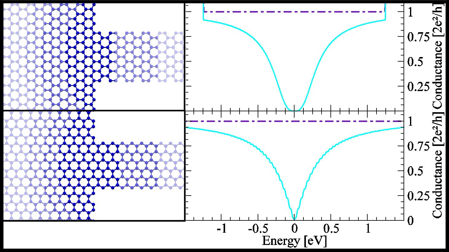
Since the associated resistance is independent of the ribbon length, this behaviour is a genuine manifestation of the contact resistance at the junction 333We are considering metallic nanoribbons. For non-metallic nanoribbons the resistance is exponentially increasing with length.. The junction conductance we have here calculated represents the characteristics of the elementary electronic diffraction barrier which is at the basis of the universal behaviour observed in all the devices hereby studied, slits, nanoribbons or quantum dots. Indeed coming back to the nanoribbon case, if in Fig. 2 we plot (dashed curve) with as extracted from Fig. 3 for the elementary junction, we find that the curve turns out to be the envelope of the Fabry-Perot oscillations minima in the nanoribbon conductance, as expected from Eq. (2). This exemplifies the concept of electronic diffraction barrier at a constriction and gives a quantitative example of such a barrier.
Conductance of a quantum dot – We now turn to more complicated structures and consider a standard nanoelectronics quantum dot (Fig. 4) consisting of a purposely irregular shape graphene nanostructure contacted via small apertures to the two half-planes graphene leads. Applying again the concept of electronic diffraction barrier, we expect that the quantum dot is weakly coupled to the leads when the energy of the electrons in the graphene sheet is close to the Dirac energy, i.e. when their wavelength is sufficiently large. We note that the conductance of this system (Fig. 4) presents a maximum around eV which is the energy of the Van-Hove singularity of bulk graphene where the density of states diverges. We also note many irregular peaks superimposed to the envelope, clearly showing characteristic resonances of the quantum dot to be associated to the particular (irregular) shape. The conductance decreases when going to the Dirac point, which is a signature of the lowest number of available states and of a diffraction barrier at the contact constrictions. The maximum to minimum transmission ratio between adjacent peaks is much larger in the vicinity of the Dirac energy than at other energies. This is also observed in the nanoribbons studied previously. Again this can be explained by the presence of two diffraction barriers at the contacts which are nearly completely reflecting () at the Dirac energy. This leads to well defined states within the quantum dot, and thus well defined conduction channels through these states. If we take as criterion to identify a range with well defined resonances the same we already introduced (maximum to minimum ratio greater than ), then we find that the critical wavelength is of order of nm for a width nm. This is the same range of values of as in nanoribbons, i.e. .
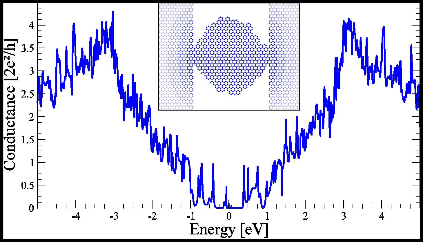
Experimental implications – Our quantum dot computed characteristics (Fig. 4) looks very similar to the experimental result of Ponomarenko et al. (Ref. Geim , Fig. 1). In those experiments the relation between voltages (here is the voltage variation with respect to the Dirac point voltage expressed in Volts) and electronic wavelength is NovoselovPrivate . From that one deduces that in their experiment the resonances are well defined for a wavelength to aperture ratio in reasonable agreement with the numerical results presented here. They reported also the low bias conductance of constrictions of 20 nm (Ref. Geim , Fig. S2), similar to the slits studied here. First of all, after our study of slits the Kirchoff-like (linear) regime is reached at voltages Volts and for higher voltages we predict for this slit a conductance . This is consistent with the experimental results and for instance at 100 Volts from the voltage corresponding to the Dirac point they measure (Ref. Geim , Fig. S2), while we predict , in good agreement with the experiment. On the other hand, the comparison of our results with their smaller nm constriction is not such good. Other mechanisms should influence the electronic transport in this case. This is in agreement with the evidence of thermally activated transport for the smaller experimental constriction.
To conclude, our work establishes an important link between nanoelectronics and subwavelength optics which could be tested in today’s technology graphene nanodevices, thank to its remarkable properties. The concept of electronic diffraction barrier is central to the understanding of transport properties in the subwavelength regime. It allowed us to get insights into the properties of graphene junctions, slits, nanoribbons, and quantum dots and explain their conductance characteristics in terms of diffraction and interference phenomena. This analogy can be further pushed forward in the design of devices with new properties.
Acknowledgements - This work has benefited from exchanges with many colleagues. We thank in particular C. Berger, X. Blase, F. Balestro, D. Feinberg, L. Lévy, L. Magaud, P. Mallet, C. Naud, T. Lopez-Rios, P. Quémerais, F. Varchon, J. Y. Veuillen, W. Wernsdorfer, L. Wirtz. Computer time has been granted by IDRIS and Ciment/Phynum.
References
- (1) L. A. Ponomarenko et al., Science 320, 356 (2008).
- (2) P.-E. Wolf and G. Maret, Phys. Rev. Lett. 55, 2696 (1985).
- (3) S. Datta, Electronic Transport in Mesoscopic Systems, Cambridge University Press, Cambridge 1995.
- (4) V. V. Cheianov, V. Fal’ko and B. L. Altshuler, Science 315, 1252 (2007).
- (5) K. S. Novoselov et al., Nature 438, 197 (2005).
- (6) Y. Zhang, Y.-W. Tan, H. L. Stormer and P. Kim, Nature 438, 201
- (7) C. Berger et al., Science 312, 1191 (2006).
- (8) S. V. Morozov et al., Phys. Rev. Lett. 100, 016602 (2008).
- (9) B. Özyilmaz et al., Phys. Rev. Lett. 99, 166804 (2007).
- (10) H. A. Bethe, Phys. Rev. 66, 163 (1944).
- (11) T. W. Ebbesen et al. Nature 391, 667 (1998).
- (12) E. Ozbay, Science 311, 189 (2006).
- (13) W. L. Barnes, A. Dereux and T. W. Ebbesen, Nature 424, 824 (2003).
- (14) P. Quémerais, A. Barbara, J. Le Perchec and T. López-Rios, J. App. Phys. 97, 053507 (2005).
- (15) Y. Takakura, Phys. Rev. Lett. 86, 5601 (2001).
- (16) J. R Suckling et al. Phys. Rev. Lett. 92, 147401 (2004).
- (17) P. R. Wallace, Phys. Rev. 71, 622 (1947).
- (18) P. Darancet, V. Olevano and D. Mayou, to be published. P. Darancet, PhD thesis.
- (19) C. Stampfer et al., Appl. Phys. Lett. 92, 012102 (2008).
- (20) I.Brezinova, C.Stampfer, L. Wirtz, S. Rotter, J. Burgd örfer, Phys.Rev.B 77, 165321 (2008).
- (21) N. M. R. Peres, A. H. Castro Neto and F. Guinea, Phys. Rev. B 73, 241403(R) (2006).
- (22) K. Nakada, M. Fujita, G. Dresselhaus and M. S. Dresselhaus, Phys. Rev. B 54, 17954 (1996).
- (23) K. S. Novoselov, private communication.