Spin polarized current and Andreev transmission in planar superconducting/ferromagnetic Nb/Ni junctions
Abstract
We have measured the tunnelling current in Nb/NbxOy/Ni planar tunnel junctions at different temperatures. The junctions are in the intermediate transparency regime. We have extracted the current polarization of the metal/ferromagnet junction without applying a magnetic field. We have used a simple theoretical model, that provides consistent fitting parameters for the whole range of temperatures analyzed. We have also been able to gain insight into the microscopic structure of the oxide barriers of our junctions.
pacs:
74.50.+r, 74.80.Fp, 75.70.-i1 Introduction
Experiments with tunnel junctions using ferromagnetic metals[1] have been an interesting topic since a long time. This subject has grown again[2] because of the new field of spintronics where spin dependent currents are an important requisite of many possible devices.[3, 4] This implies that control and measurements of spin polarized currents are needed. Spin-polarized electron tunnelling[5] is a key tool to measure the current polarization and to understand the physics involved in these effects. Most of the recent experimental works have focused on the suppression of the Andreev reflection and have used the point contact geometry with a superconducting electrode[6, 7]. However the local information extracted by point contact or scanning tunnelling microscope techniques seems to be less suitable for devices than planar tunneling junctions. In addition, the intrinsic difficulty of fabricating a perfect uniform oxide layer can jeopardize the latter technique. Recently Kim and Moodera[8] have reported a large spin polarization of 0.25 from polycrystalline and epitaxial Ni (111) films using Meservey and Tedrows’s technique[5] and standard Al electrode and oxide barriers, that allows for an almost ideal barrier behaviour.
In this work we show that the current polarization of ferromagnets can be extracted without applying a magnetic field to the junction and using an oxide barrier that is far from ideal. The experimental data are obtained for Nb/NbxOy/Ni planar tunnel junctions, where the barrier is fabricated using the Nb native oxides. In this case, different NbxOy oxides are present in the barrier. This fact usually prevents the analysis of the dV/dI characteristics in terms of perfect tunnelling. Indeed, we show below that our junctions are neither in the tunnelling nor in the transparent regime, but rather in a regime intermediate between both. We shall argue that the current polarization can be obtained even in this intermediate regime by use of a simple model.
2 Experimental method
Nb(110) and Ni(111) films, grown by dc magnetron sputtering, were used as electrodes. The structural characterization of these films was done by x-ray diffraction (XRD) and atomic force microscopy (AFM), see for instance Villegas et al.[9] Briefly, the junction fabrication was as follows: First, a Nb thin film of 100 nm thickness was evaporated on a Si substrate at room temperature. An Ar pressure of 1 mTorr was kept during the deposition. Under these conditions, the roughness of the Nb film, extracted from XRD and AFM, is less than 0.3 nm[9] and superconducting critical temperatures of 8.6 K are obtained. After this, the film was chemically etched to make a strip of 1 mm width. A tunnel barrier was prepared by oxidizing this Nb electrode in a saturated water vapor atmosphere at room temperature.[10] The thickness of the oxide layer, extracted from the simulations performed with the SUPREX program,[11] is 2.5 nm. X-ray photoelectron spectroscopy analysis performed in these oxidized films reveals that dielectric Nb2O5 is the main oxide formed. There are also other oxides, such as metallic NbO, but in much less amount. Taken into account Grundner and Halbritter studies,[10] Nb2O5 is the outermost oxide layer on Nb, whereas NbO is located closer to the Nb film. The characterization by AFM reveals a RMS roughness of around 0.7 nm. A detailed account of the structural and compositional characterization of the barrier has been reported elsewhere.[12]
On top of this film (Nb with the oxide barrier), the second electrode of Ni was deposited under the same conditions as Nb (up to 60 nm thickness) using a mask to produce cross strips of 0.5 mm width, so that the overlap area of the two electrodes is 0.5 mm2.
Junctions fabricated using these materials and geometry, will not show a good tunneling behaviour, neither a point-contact behaviour. As we will see, the junctions will lie on the intermediate regime.
Perpendicular transport in tunnelling configuration was investigated by means of characteristic dynamic resistance () versus voltage () using a conventional bridge with the four-probe method and lock-in techniques. The measured lock-in output voltage was calibrated in terms of resistance by using a known standard resistor.
We have measured the conductance, defined as the inverse of the differential resistance , of three different tunnel junctions. Moreover, junction 1 (J1) has been measured and analyzed at temperature K, junction 2 (J2), at temperatures and K, and junction 3 (J3), at temperatures , and K. These measurements have allowed us to access and assess the behavioiur and quality of our samples in the low (J1 and J2) and intermediate (J2 and J3) temperature range of this heterojunction. Each data set presented in this article has been normalized with respect to the background conductance of the corresponding junction.
3 Theoretical Models
3.1 Introduction
The conductance across a normal/superconducting junction may be expressed in terms of the reflection probabilities of quasiparticles transversing the junction, and of Andreev processes as
| (1) |
where is the Fermi function; and is the applied voltage.
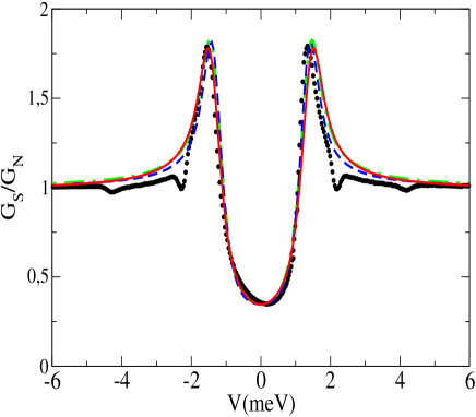
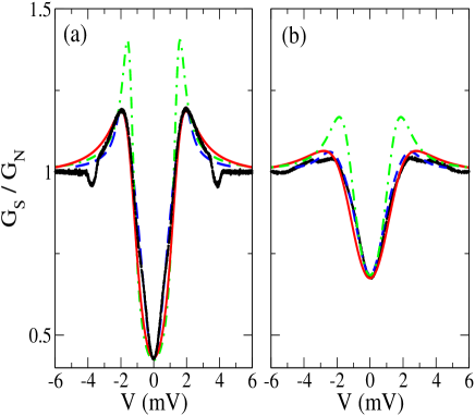
Andreev reflection processes are proportional to the square of the conventional transmission coefficient of the barrier, , and therefore are strongly suppressed for highly resistive barriers. Junctions with transmission coefficients smaller than about 0.1 show small subgap conductances, and can be classified as belonging to the tunneling regime. Our experimental results, shown as black circles in 1 and 2, exhibit a significant conductance below the superconducting gap even at the lowest temperatures. Therefore we expect that our effective oxide barriers should be neither too high nor too thick, and we classify them as belonging to an intermediate transparency regime.
While there are fairly complete descriptions of the transmission across ferromagnet/superconducting junctions[13, 14], we have decided to describe it by three models that share the virtue that are conceptual and algebraically simple. These models are: i) The generalization of the Blonder-Tinkham-Klapwijk (BTK) model [15] to ferromagnetic electrodes proposed by Strijkers and coworkers;[16] ii) a description of the effects of a finite current polarization in terms of spin dependent transmission coefficients, as discussed by Pérez-Willard et al;[17] and iii) a very simple generalization of the BTK model to ferromagnetic electrodes with finite bulk magnetization.
We define the current polarization as the imbalance between the current intensity of majority and minority carriers[7] in a metal/ferromagnet junction, measured when the voltage tends to zero,
| (2) |
where both spin channels contribute equally to the total current intensity and conductance.
3.2 Strijkers’ model (Model I)
Strijkers’ model uses as adjustable parameters the current polarization , the height of barrier ,[18] which is modeled by a delta function, and the size of the superconducting gap at the interface .
The process of electron transfer across the junction is splitted into a fully polarized channel, for which the Andreev reflection coefficient is zero, and
| (5) |
where and are the coherence coefficients of the superconducting wave function; and a paramagnetic channel described by the coefficients and of the BTK model in its conventional form.[15]
The total conductance is then written in terms of the conductance of the fully polarized channel () and the conductance of the paramagnetic channel ():
| (6) |
This model interpolates between the paramagnetic case (BTK model), and the half metal, where it predicts correctly that the amplitude for Andreev reflection vanishes.
3.3 Simple quasiclassical theory (Model II)
We now use a simple model based on quasiclassical theory,[20, 21, 22, 19] in which boundary conditions have been dumped into the spin-dependent transmission coefficients [17]. The conductance for each spin channel in this model is determined by
| (7) |
where the effective reflection coefficients depend now on spin. These can be expressed in terms of the normal and anomalous components of the Green’s function, evaluated right at the superconducting side of the interface, as follows
| (8) |
where the reflection amplitude of the barrier satisfies the sum rule .
The explicit functional form of and may be obtained from the equation of motion of the quasiclassical Green function that, for a bulk superconductor, reduces to
| (9) |
where disorder and pair breaking effects, parametrized by the Dynes parameter ,[23] are dealt within the t-matrix approximation. Eq. (5) is used to fit the conductance data, using the two transmissions , and as adjustable parameters.
Eqs. (7) can also be solved when the gap is zero. This gives and , and corresponds the solution for the normal state. Then, the conductance per spin chanel is, simply, , and the current polarization is obtained from it as
| (10) |
Perez-Willard et al.[17] used this model to analyze Al/Co point contacts, where the proximity effect may be discarded since the size of the junction is negligible compared with the coherence length. They indeed found close agreement with their experimental data for a wide range of temperatures.
| Junction | T (K) | (meV) | (meV) | ||||
|---|---|---|---|---|---|---|---|
| 1 | 1.52 | 0.60 | 0.30 | 0.45 | 0.33 | 1.36 | 0.00 |
| 2 | 1.5 | 0.72 | 0.30 | 0.51 | 0.41 | 1.20 | 0.38 |
| 2 | 3.95 | 0.90 | 0.35 | 0.62 | 0.44 | 1.13 | 0.7 |
| 3 | 4.53 | 0.53 | 0.50 | 0.52 | 0.03 | 1.18 | 0.4 |
| 3 | 5.00 | 0.43 | 0.40 | 0.42 | 0.04 | 1.10 | 0.5 |
| 3 | 5.39 | 0.43 | 0.35 | 0.39 | 0.10 | 1.10 | 0.5 |
3.4 Generalization of BTK model for a ferromagnetic electrode (Model III)
We finally introduce ferromagnetism through an exchange splitting in one of the electrodes. Hence, wave-vectors depend on spin as
| (11) |
The barrier is modeled as a function of height Z. The normal and Andreev reflection probabilities, which depend on the spin flavour, can be calculated from
| (12) |
where the coefficient is equal to
| (13) |
, the wave-vector is simply and is a parameter measuring the strength of the barrier. We introduce disorder in a phenomenological fashion,[23] by adding an imaginary part to the energy, .
The conductance per spin channel can be calculated in the same way as in the BTK model using[24]
| (14) |
This model only depends on the four ratios and , but we prefer to fix instead of letting it dissapear by an adequate change of variables. We therefore set eV, guided by our Ab initio simulation of Ni, performed with the Molecular Dynamics suite SIESTA [25]. We have also taken eV as representative of the spin-splitting of nickel along our experimental direction. The prefactor in front of the Andreev reflection amplitude is therefore set to from the outset.
The parameters , and are on the contrary adjusted so that formula (12) provide accurate fits to the conductance data. Once this is achieved, the current polarization at a given temperature is estimated by using again formula (12), but now with the gap set to zero.
| (15) |
where
| (16) |
are the transmission probabilities of each spin channel in the normal state.
4 Discussion
4.1 Comparison of theoretical models
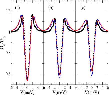
We plot the normalized conductance of J1, J2 and J3, as a function of voltage in Figs. 1, 2 and 3, respectively. J1, that has been measured at K, shows well developed coherence peaks. On the contrary, J2 and J3 do not display them even at low temperatures. We have tried to fit the height and position of the coherence peaks, as well as the height as shape of the low voltage conductance with the three models described above. We have not focused on the features that happen outside the gap in the curves, as physics in this region is controlled by magnons and phonons, while inside the gap physics is controlled by Andreev processes, which determine the current polarization and do not interphere with phonon processes.
We have been able to fit J1 with Model I, but have failed to fit any of the conductance data of J2 and J3 with that model, that invariably gives too high coherence peaks, probably due to its oversimplified description of ferromagnetism and the neglect of disorder effects. This is explicitly shown in Figs. 1 and 2.
We have been able to fit with Model II very accurately the conductance of junctions 1 and 2 for all temperatures. On the contrary, we have failed to fit the low voltage data of J3 at temperatures and 5.39 K, as shown in Fig. 3. Moreover, the fits to J2 and J3 provide transmission coefficients that show a marked dependence with temperature, as shown in Table I. Indeed, while remains essentially constant for a given junction, the spin-averaged transmission varies strongly with temperature. This is not physically correct, since the transmission coefficients should show appreciable modifications only for temperature changes of the order of the bandwidth energy. A closer look at the results presented in the table reveals that Model II gives a current polarization that is unreasonably small for J3.
| Junction | (K) | Z | (meV) | (meV) | |||
|---|---|---|---|---|---|---|---|
| 1 | 1.52 | 1.15 | 0.475 | 0.365 | 0.13 | 1.44 | 0.01 |
| 2 | 1.5 | 3.02 | 0.115 | 0.078 | 0.19 | 1.44 | 0.57 |
| 2 | 3.95 | 3.02 | 0.115 | 0.078 | 0.19 | 1.40 | 1.0 |
| 3 | 4.53 | 2.00 | 0.228 | 0.161 | 0.17 | 1.35 | 0.35 |
| 3 | 5.00 | 2.00 | 0.228 | 0.161 | 0.17 | 1.35 | 0.35 |
| 3 | 5.39 | 2.00 | 0.228 | 0.161 | 0.17 | 1.35 | 0.35 |
It is also apparent from the table that Model II provides values for the superconducting gap that are too small, and actually do not seem to follow the temperature dependence expected for a BCS superconductor. For instance, the model predicts a zero-temperature gap for J3, meV. Using the measured critical temperature, we find that the ratio is equal to 3.25, which is much smaller than that of bulk Nb (3.8).
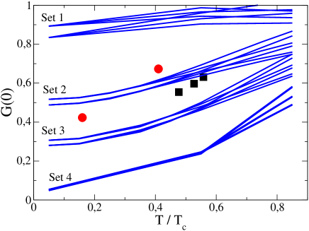
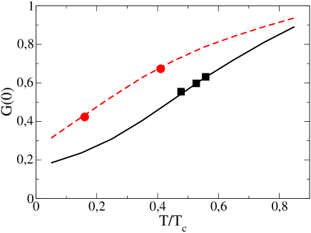
To understand better why the model fails to fit the zero voltage conductance of J2 and J3, we plot in Fig. 4 for several sets of the parameters , and , that cover most of the parameter space. We have chosen for the values 0.1, 0.4, 0.55 and 0.7. For each , we have taken two representative values of (0.15 and 0.35) and three different values of , (0.1, 0.3 and 0.5). The figure shows that the 24 curves cluster in four different sets, according to the value of . This implies that the value and temperature dependence of the zero-voltage conductance is determined in this model essentially by the average transmision. The figure demonstrates in any case that the experimental values of for junctions J2 and J3 show a stronger dependence with temperature than the estimates provided by Model 2. We therefore believe that the model, while very appealing due to its simplicity, is actually too simple to describe the physical behavior of these junctions that belong to the intermediate transparency regime and have been measured at low and intermediate temperatures.
We turn the attention now to our generalized BTK model (Model III). We note that the model is able to fit well the conductance data of junctions 1 and 2. In addition, it also provides a good fit to the data of J3, in contrast to the quasiclassical model. More importantly, the model provides a temperature-independent barrier height , that translates into temperature-independent transmission coefficients (see Table II). The values of Z so obtained allow us to clasify the junctions in an intermediate regime between tunnelling and point contact. Junction 2 is actually the closest to the tunneling regime, while Junction 1 is closest to the transparent regime. Junction 3, that we failed to fit with model II, lies well within this intermediate regime. Fig. 5 clearly demonstrates that our model provides a temperature dependence of that fits well the experimental data.
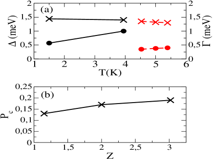
Fig. 6 (a) shows the temperature dependence of the gap obtained in the fits performed with Model III. We find values for the gap slightly smaller than those of bulk Nb, but consistent with the measured critical temperature and with the conventional temperature dependence of a BCS superconductor. The extrapolated zero-temperature gap, meV, provides a superconducting ratio in close agreement with the ratio for Nb, 3.8.
Fig. 6 (a) also shows the temperature dependence of the disorder parameter. We find that shows a smooth and linear dependence within the studied range of temperatures. The values of are large, as should be expected, since our Nb samples are highly disordered.
We plot in Fig. 6 (b) the current polarization obtained using model III, as a function of the height of the barrier Z. We find that increases with Z from 0.13 to 0.19, which shows that the current polarization increases with the tunelling quality of the junction. We note that Soulen et al. [7] have found polarizations of about 45% using Ni/Nb junctions in a point contact geometry. More recently Kim and Moodera [8] have performed experiments for Ni/Al plannar tunnel junctions. They have found that grows from 11% to 33% as the tunneling quality of the junctions increases. Our theoretical calculations confirm that should increase with the strength or the thickness of the tunneling barrier.
The preceding analysis shows that the main advantage of model III (BTK) over model II (adjustable spin dependent transmission coefficients) is the stronger dependence on temperature of the conductance in model III. The main difference between the two models lies in the description of the ferromagnetic electrode. Model III uses two different Fermi surfaces, one for each spin. Hence, the proximity effect is suppressed, reducing the Andreev reflection at low temperatures.
5 Summary and conclusions
We have fabricated and measured fairly large and far from ideal superconducting/ferromegnetic tunel junctions. A simple theoretical model allows us to extract tunnelling related parameters for such junctions. We have grown Nb/NbxOy/Ni planar tunnel junctions, and measured its conductance at different temperatures. We have found that they belong to the regime of intermediate transparencies. We have been able to fit the conductance curves with a simple generalization of the BTK model,[15] that provides a sensible set of temperature-independent transmission probabilities. Our calculations suggest that the results can depend significantly on the description of the bulk ferromagnetic electrode, as Andreev reflection depends both on the barrier transmission coefficients and on the exchange field inside the ferromagnet. We have been able to give reasonable values of the current polarization without the need to apply a magnetic field. We have also studied the relationship between these two quantities, showing that the current polarization depends significantly on the height of the barrier. This simple generalization of the BTK Model to a superconducting/ferromagnetic junction could be improved considering a 3D Model. However, we have shown that the simple one dimensional model can fit the experimental data and also provides good estimates of the current polarization.
Acknowledgments
We wish to thank very useful discussions with J. Moodera, M. Eschrig and M. Fogelstrom. This work was supported by MEC (MAT2002-04543, MAT2002-12385E, MAT2002-0495-C02-01, BFM2003-03156 and AP2002-1383), and CAM (GR/MAT/0617/2004). Additionally, E.M.G. acknowledges Spanish Ministerio de Educación y Ciencia for a Ramón y Cajal contract, and R. Escudero thanks Universidad Complutense and Ministerio de Educación y Ciencia for a sabbatical professorship. A.D.-F. thanks Ministerio de Educación y Ciencia for a FPU grant (AP2002-1383).
References
References
- [1] J. E. Christopher, R. V. Coleman, A. Isin, and R. C. Morris, Phys. Rev. B 172, 485 (1968).
- [2] B. J. Jonsson-Akerman, R. Escudero, C. Leighton, and Ivan K. Schuller, Appl. Phys. Lett. 77, 1870 (2000)
- [3] G. Prinz, Phys. Today 48, 58 (1995).
- [4] J. de Boeck, Science 281, 357 (1998).
- [5] R. Meservey and P. M. Tedrow, Phys. Rep. 238, 173 (1994).
- [6] S. K. Upadhyay, A. Palanisami, R. N. Louie, and R. A. Buhrman, Phys. Rev. Lett. 81, 3247 (1998).
- [7] R. J. Soulen Jr., J. M. Byers, M. S. Osofsky, B. Nadgorny, T. Ambrose, S. F. Chen, P. R. Broussard, C. T. Tanaka, J. Nowak, J. S. Moodera, A. Barry, and J. M. D. Coey, Science 282, 85 (1998).
- [8] T. H. Kim, and J. S. Moodera, Phys. Rev. B 69, 020403(R) (2004).
- [9] J. E. Villegas, E. Navarro, D. Jaque, E. M. González, J. I. Martín, and J. L. Vicent, Physica C 369, 213 (2002).
- [10] M. Grundner and J. Halbritter, Surface Science 136, 144 (1984).
- [11] E. E. Fullerton, I. K. Schuller, H. Vanderstraeten, and Y. Bruynseraede, Phys. Rev. B 45, 9292 (1992).
- [12] E. M. Gonzalez, F. J. Palomares, R. Escudero, J. E. Villegas, J. M. Gonzalez, J. L. Vicent J. Magn. Magn. Mat. 286, 146 (2005)
- [13] M. Eschrig, Phys. Rev. B 61, 9061 (2000).
- [14] J. Kopu, M. Eschrig, J. C. Cuevas and M. Fogelström, Phys. Rev. B 69, 094501 (2004).
- [15] G. E. Blonder, M. Tinkham, and T. M. Klapwijk, Phys. Rev. B 25, 4515 (1982).
- [16] Y. Ji, G. J. Strijkers, F. Y. Yang, and C. L. Chien, Phys. Rev. B 64, 224425 (2001).
- [17] F. Pérez-Willard, J. C. Cuevas, C. Surgers, P. Pfundstein, J. Kopu, M. Eschrig, and H. v. Lohneysen, Phys. Rev. B 69, 140502(R) (2004).
- [18] The height of the barrier Z in BTK’s model is related to its reflection coefficient in the normal state R, by .
- [19] J. W. Serene and D. Rainer, Phys. Rep. 101, 221 (1983).
- [20] W. Belzig, A. Brataas, Y. V. Nazarov and G. E. W. Bauer, Phys. Rev. B 62, 9726 (2000).
- [21] J. P. Morten, A. Brataas and W. Belzig, Phys. Rev. B 70, 212508 (2004).
- [22] Z. Jiang, J. Aumentado, W. Belzig and V. Chandrasekhar, cond-mat/0311334 (2003).
- [23] R. C. Dynes, V. Narayanamurti and J. P. Garno, Phys. Rev. Lett. 41, 1509 (1978).
- [24] A. A. Golubov, Physica C 326-327, 46 (1999).
- [25] J. M. Soler, E. Artacho, J. D. Gale, A. G. Junquera, P. Ordejón, and D. Sánchez Portal, Journal of Physics: Condensed Matter 14,2745 (2202).