Incoherent Cooper pair tunneling and energy band dynamics in small Josephson junctions
Abstract
We discuss the properties of devices of small Josephson junctions in the light of the phase fluctuation theory and the energy band structure, which arises from the delocalization of the phase variable. The theory is applied in the realization of a mesoscopic amplifier, the Bloch oscillating transistor. The device characteristics and comparison with theory and simulations are discussed. The current gain of the device in a stable operating mode has been measured to be as high as 30. Measurements on input impedance and the power gain show that the BOT is an amplifier designed for middle-range impedances, ranging from .
pacs:
73.23.Hk 74.50.+r 73.23.-b1 Introduction
The conjugate nature of charge and phase gives rise to a rich array of physical phenomena, which have been intensively studied both theoretically and experimentally. The quantum nature of the phase variable was shown in macroscopic tunnelling experiments clarke and its conjugate relationship to the charge has been shown in many consequent studies Tinkham1996 .
One of the consequences of the charge-phase conjugate relationship is the Coulomb blockade of Cooper pairs which arises in very small Josephson junctions haviland91 . The system is described in phase or charge space, depending on which variable is a good quantum number and, consequently, determines the eigenstates of the quantum system. Associated with the two variables are two competing energy scales, the charging energy and the Josephson coupling energy . The Hamiltonian for the small Josephson junction has a periodic potential, hence, Bloch states and a corresponding energy band structure can be derived analogously with the conduction electrons in solid state physics Kittel ; LZ .
Incoherent tunnelling, the interaction of tunnelling electrons or Cooper pairs with the electromagnetic environment, is a strong effect observed in small tunnel junctions both in the normal and superconducting states devoret90 ; holst94 . Small tunnel junctions can be used as sensitive detectors of environmental impedances and noise sources but, this sensitivity also means that attention to control of the electromagnetic environment is essential when designing mesoscopic devices.
The Bloch Oscillating transistor is a mesoscopic device which is based on the dynamics of the Bloch bands in a voltage biased Josephson junction (JJ) in a resistive environment. The main operating principle was demonstrated in references delahaye2 ; delahaye1 ; hassel04a ; hassel04 . The conclusions that can be drawn from these articles is that the BOT shows considerable current and power gain (for both cases ). Additionally, the noise temperature at the optimum operation point was observed to be as low as 0.4 K, although, the theoretical and simulated noise temperature has been shown to be 0.1 K or even below. The BOT has an input impedance, which can fairly easily be tailored by fabrication to be in the range . Thus, the BOT is a device suitable for use at mid-range impedances and it complements the group of basic mesoscopic devices: the single-electron transistor (SET) - a device for high-impedance applications and the SQUID, a low impedance device.
At this point, we would like to emphasis that one should not confuse the BOT device with the Bloch transistor AL , which is a similar but, fundamentally, a different kind of JJ device where the current of a single Cooper pair transistor (SCPT) is modulated by a gate voltage.
This paper will briefly review the physics that gives rise to the voltage-current relation of the Josephson junction in light of both the Bloch band model and incoherent Cooper pair tunnelling. After the theory, a few observations on the ”Bloch nose” - a consequence of Bloch Oscillations - will be presented. The last part of the paper will take on a more device oriented approach with the discussion of the experiments and the question how well the findings can be reproduced by theoretical simulations on the Bloch Oscillating Transistor.
2 Theory
2.1 Theory of Bloch states
In mesoscopic systems the phase and charge comprise a conjugate pair of quantum variables, analogously with the more familiar space and momentum coordinates. The variables thus satisfy the commutation relation
| (1) |
The total classical Lagrangian for a single, isolated Josephson junction can be written as
| (2) |
which consists of the charging energy due to the capacitance and the Josephson coupling energy as the potential. From the commutation relation (1) we can immediately write the quantum mechanical Hamiltonian LZ as
| (3) |
where also the interaction between the driving current and the phase variable , the junction environment energy and the coupling with the environment have been included. Depending on the theoretical framework used, some, or none of the last three terms are included.
To set the initial stage, we consider only the first two terms in the Hamiltonian, in the case when and the charge is a good quantum number, thus leading to Coulomb blockade of Cooper pairs and a complete delocalization of the phase. Equation (3) then takes the form of the familiar Mathieu equation with the well-known solutions of the form , where is a -periodic function and the wave functions are indexed according to band number and quasicharge quasicharge . More precisely, the Mathieu equation has also periodic solutions, which correspond to the the case of quasiparticle tunnelling Schon . The resulting energy band structure is illustrated in Fig. 2. Verification of the existence of the energy bands has been carried out by different methods prance92 ; flees97 ; lindell03 .
For the opposite limit, , we should index the system eigenstates according to the phase variable and the charge would be completely delocalized. This situation corresponds to the classical superconducting state of the Josephson junction, which can also be described in the ”tilted washboard” picture when including the third term, in the Hamiltonian (3). This model can be easily extended to the well known resistively and capacitively shunted junction (RCSJ) model, where one includes a dissipative resistor in the circuit. But, we will not discuss or apply the RCSJ model in this paper as it is mostly used in the case of large Josephson junctions in the context of macroscopic quantum tunnelling.
Next, we consider the Josephson junction in the band picture, when the phase is delocalized and the state of the system can be described by its quasicharge . For a more realistic situation, we also need to consider the junction’s coupling to its environment. The detailed and involved calculations for the cases with ohmic and quasiparticle dissipation can be found in Refs. LZ ; Schon . The physics is rich in detail and includes phenomena such as the zero-dimensional quantum phase transition when the system goes from a superconducting to an insulating state Penttila1999 .
The instantaneous voltage over the junction is given by
| (4) |
We consider the system to be either current or voltage biased, meaning that the environmental resistor is situated in parallel or in series with the junction (see Fig. 1). With a steady current flowing through the junction the quasicharge evolves according to
| (5) |
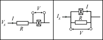
In the voltage biased case, the voltage over the total system consists of the voltage drop over the series resistor and the junction voltage
| (6) |
In the current biased case, where the resistor is parallel with the junction, we have the relation for the total current
| (7) |
Hence, one can switch between these two cases if one defines
In practice, we fabricate the resistor in series with the junction, and thus consider next the former case of voltage bias. If the resistor is large (compared to the CB resistance of the junction), we can still think of the junction itself to be current biased. Hence, if the driving current is low enough, , where is the gap between the first and second band, the quasicharge is increased adiabatically and the system stays in the first band. We are then in the regime of Bloch oscillations; the voltage over the junctions oscillates and Cooper pairs are tunnelling at the borders of the Brillouin zone, or as for the definitions here (see Fig. 2), at . Consequently, the current through the junction is coherent and the voltage and charge over the junction oscillate with the frequency
| (8) |
The theoretical characteristics for an external current bias thus first shows an increase of the junction voltage with increasing current but at the onset of Bloch oscillations, the voltage decreases. If the current is not adiabatically small, we can have Zener tunnelling between adjacent energy bands. The tunnelling is vertical, i.e the quasicharge does not change. The probability of Zener tunnelling between bands and when is given by
| (9) |
where and is the Zener break down current ben-jacob .
The downward transitions can take place through several processes. The cases we need to consider are transitions due to quasiparticle tunnelling and due to charge fluctuations caused by the environment. The quasiparticle transitions in the JJ couple states that differ by one . In the BOT, the transitions are primarily driven by a current bias through a second junction, explicitly designed for returning the system to the lowest band. The external environment gives rise to e.g. current fluctuations that couple linearly to the phase variable. These can cause both upwards and downwards transitions. The strength of the fluctuations is given by the size of the impedance: the larger the impedance the smaller are the current fluctuations and the transitions rates. As we will see later on, the successful operation of the BOT requires one to control both the upwards and downwards transition rates, or rather their relative strength. Later, when discussing a very simple BOT model, we will make use of the Zener transition rates and transitions due to charge fluctuations, both derived in Ref. Schon .
2.2 Incoherent tunneling and phase fluctuation theory
It is well known that the electromagnetic environment of tunneling junctions affects the tunneling process by allowing exchange of energy between the two systems formed by the tunnel junction and the external circuit devoret90 ; averin ; girvin ; IN . The influence of the external circuit can be taken into account, for example, within the so called -theory, which is a perturbation theory assuming weak tunneling. The external environment is thought of as consisting of lumped element electric components which give rise to a classical impedance . The impedance is quantized using the Caldeira-Leggett model, which consists of an infinite number of LC-oscillators. Hence, in this limit, one can model dissipative quantum mechanics. The energy fed into the bath never returns to the tunnel junction system.
A perturbative treatment of the Josephson coupling term gives rise to a simple looking result for incoherent Cooper pair tunneling averin ; IN . The forward tunneling rate is directly proportional to the probability of energy exchange with the external environment:
| (10) |
and the backward tunneling rate is , thus leading to the total current
| (11) |
The function can be written as
| (12) |
which is a Fourier transform of the exponential of the phase-phase correlation function
| (13) |
The phase-phase correlation function is determined by the fluctuations due to the environment and it can be related to the environmental impedance with the fluctuation-dissipation theorem. The result is that can be found by
| (14) |
where , and
| (15) |
is the impedance seen by the junction.
We also need to consider quasiparticle tunneling, especially in the BOT circuit, where we also have an NIS junction. We will not, however, take into account Cooper pair transfer by Andreev reflection Andreev1965 as it is not essential in the experiment. For quasiparticles the perturbative tunneling rate assumes the form
| (16) |
Here, the density of states on the two sides of the junction depend on whether the lead, or 2, is normal or superconducting. In the superconducting region, we have , for and zero otherwise, and in the normal region .
2.3 BOT conceptual view
The circuit schematics and a conceptual view of the BOT operation cycle are shown in Fig. 2. The basic circuit elements are the Josephson junction, or SQUID, at the emitter, with a total normal state tunnel resistance of , the single tunnel junction at the base with the normal state resistance , and the collector resistance . The BOT base is usually current biased with a large resistance at room temperature, but the large stray capacitance results in an effective voltage bias. A requirement for the successful BOT operation is that the charging energy is of the same order of magnitude as the Josephson energy . For the theory presented in this paper to be valid, the condition has to be satisfied.
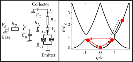
The theory describing the workings of the BOT is outlined in articles hassel04a ; delahaye2 ; hassel04 . The work by Hassel and Seppä hassel04 , contains both an analytical approximation of the physics and the basic principles for a simulation which are also used to some extent in this paper to test the agreement between the experiment and simulation.
The basic physical principle of the BOT relies on the existence of Bloch bands in the JJ, which is embedded in a resistive environment . The BOT is voltage biased to a point on the lowest band where Bloch oscillations can start. The supercurrent thus flows due to coherent Bloch oscillations (see Fig. 2) in the lowest band until the flow is stopped by Zener tunneling into the second band. The JJ is Coulomb blockaded until it relaxes down to the first band, either intrinsically due to charge fluctuations caused by the environmental resistance or with a controlling quasiparticle current. The intrinsic relaxation is detrimental for BOT operation and thus the fluctuations should be kept low by requiring that . In practice, we need to be close to the ideal operation as outlined here. The control current is injected through the second junction, which in our case is a normal-insulator-superconductor (NIS) tunnel junction. The amplification mechanism can, in its simplest form, be said to arise from the number of Bloch oscillations triggered by one quasiparticle. The Coulomb blockade of Cooper pairs (CBCP) is thus a necessity for the BOT to function.
Our simulation of the BOT is based on the method given in Ref. hassel04 . In the simulation it is assumed that the current flowing in the different parts of the BOT: the JJ, NIS junction and resistor can be treated separately and the dynamics of the island charge (, where is the capacitance of the Josephson junction and is the island voltage indicated in Fig. 2) is simulated and averaged over a large number of steps (typically 10 - 100 million). The tunneling rates or, rather, the tunneling probabilities in the JJ and NIS are calculated using the -theory IN described earlier. Furthermore, we assume the same resistive environment for both junctions. The capacitance in Eq. 15 is then . The tunneling at each point in time is then determined by comparing a random number and the tunneling probability of the different junctions, which depends on the voltage across them. Furthermore, the simulation actually assumes that and that the energy bands can be approximated by parabolas: . In this case, the quasicharge is equal to the real island charge , which is, according to the model in Fig. 2 also the charge over the Josephson junction. The equation for the simulated island charge is then given by
| (17) |
Here the collector voltage takes the role of in the theory of Bloch oscillations considered earlier and is the island voltage. The island charge is thus modified by four terms: the constant relaxation current through the collector resistor, the quasiparticle tunneling through the base junction () and JJ (), and the Cooper pair tunneling in the JJ. The theory thus excludes any quantum mechanical interactions between the Josephson and NIS junctions. This simplification has shown to be quite useful in determining the main operation principles of the device. Although, one can argue that this simple treatment of the island voltage as a time dependent variable while the tunneling rates are unaffected by island dynamics is not the correct way. As pointed out in Ref. sonin , the average fluctuations of the phase of the island will govern the tunneling in the Josephson junctions and, therefore, a more rigorous approach would account for the peculiar phase fluctuations from the tunneling quasiparticles. Nevertheless, time dependent -theory should provide a reasonable starting point when the environmental impedance is large soninPRL . However, how to include the Zener tunneling and the dynamics of the Bloch bands into the phase fluctuation model is still under investigation.
2.4 Alternative analytical theory
The physical principle of the BOT current gain can also be derived analytically from another viewpoint delahaye1 . The average BOT emitter current can be thought of as the result of being in either of the two states: the Bloch oscillation state with a time-averaged constant current and the blockaded state with zero current:
| (18) |
The amount of time the system spends in each state is given by the Zener tunneling rate, , the intrinsic relaxation , and the quasiparticle driven relaxation . The base current, however, flows during the opposite times:
| (19) |
From these equations we can simply derive the average emitter and base currents
| (20) |
| (21) |
From Eq. (21) we can solve for and insert this into Eq. (20) in order to find the emitter current
| (22) |
We thus find the current gain
| (23) |
The base current relaxes through the collector resistance and, therefore, the collector and emitter gains are related by
| (24) |
The current gains are defined with the minus sign for convenience, because, both theoretically and empirically, with the sign convention used here the derivatives are negative.
Next, we have to find the transitions rates and as a function of the collector voltage. These have been calculated by Zaikin and Golubev zaikin . The Zener tunneling rate in a resistive environment, and with the assumption , is given by
| (25) |
and the down relaxation rate due to charge fluctuations is given by
| (26) |
where , and
| (27) |
The voltage is naturally related to the Zener break down current . Equations (25) and (26) are given as function of the bias voltage , although, the theory is strictly valid for the current bias case. One can switch from the current biased to voltage biased case by doing the transformation as discussed earlier by setting . In our experiment, the relevant case is the voltage biased one.
Closed forms for the charge fluctuations in a resistive environment can be found in the two limits of thermal and quantum fluctuations:
where . At the low temperature limit where quantum fluctuations dominate one needs to know the cut-off frequency , which depends on the details of the external impedance . In practice, our experiments are done in a regime where , where both effects are present.
The two-state model presented here has also been used for the basic mechanism that generates the output noise of the BOT hassel04 . The noise of the device is found to be output governed and the input current noise is, therefore, inversely proportional to the current gain lindell2005 .
3 Fabrication and measurement
| BOT # | |||||||
|---|---|---|---|---|---|---|---|
| 1 | 90 | 24 | 188 | 0.28 | 0.93 | 0.3 | 0.03 |
| 2 | 53 | 8.8 | 368 | 0.37 | 0.78 | 2.1 | 1.8 |
The fabrication of the BOT is done using standard electron beam lithography and 4-angle shadow evaporation. The order of the evaporation process was chromium (1), aluminum (2), oxidization (3), chromium (4), copper (5) and aluminium (6). Originally, the BOT device was thought to have an NIN junction as base junction, but the technique of manufacturing both SIS and NIN junctions on the same sample has not yet been mastered, therefore, we used NIS junctions instead. In the first design, the NIS junction consisted of the aluminium-aluminumoxide-copper interface, but it turned out to be the most sensitive part of the device and it often was already broken after bonding to sample holder. An additional, 7 nm thick chromium layer, seemed to protect the junction and improved the sample yield considerably.
Instead of having a single JJ at the emitter we made two junctions, which thus form a SQUID loop. The SQUID configuration gives the possibility of tuning the effective Josephson coupling energy according to
| (28) |
where and are the Josephson energies for the two junctions, is the externally applied magnetic flux perpendicular to the loop area and is the quantum of flux. The tuning allows us to find the optimal operation point in terms of the current gain delahaye2 as well as giving the possibility to compare the dependence with the theories presented in this paper. In practice, the asymmetry of the SQUID junctions makes the tunability less than perfect as can be noted from Table 1.
The BOT measurements were done on two different dilution refrigerators: a plastic dilution refrigerator (PDR-50) from Nanoway and the other from Leiden Cryogenics (MNK-126-500). Both had a similar base temperature of 30 mK. The filtering in the PDR consisted mainly of 70 cm long thermocoax cables on the sample holder. Also, micro-wave filters from Mini-circuits (BLP 1.9) were used at room-temperature. In the Leiden setup, besides the 1 m long thermocoax on the sample holder, additional powder filters (provided by Leiden Cryogenics) were present. Similar measurement results were achieved with both setups, although the effective temperature of the sample, deduced from the zero bias resistance, was somewhat lower with the Leiden setup: 45-60 mK as compared to 80-100 mK with the Nanoway setup (see e.g. Ref. lindellPRL ).
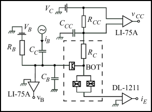
The measurement set-up used in this work is shown in Fig. 3. Most of the complexity comes from the requirements of the power gain measurement, which will be presented in Sec. 4.2.4. The BOT base is DC current biased by a large resistor , which is located at room temperature. The size of the resistor was typically G. For differential measurements, an AC-signal is fed through a coupling capacitor , in order to circumvent the large biasing resistor. Voltages are measured with low noise LI-75A voltage amplifiers and their output is fed into EG & G Instruments 7260 DSP lock-in amplifiers. An additional, surface-mount resistor, , is located on the sample holder, a few cm from the chip. Therefore, this resistor is initially also at base temperature. The role of the resistor is to act as load to the BOT, in order to allow a clear measurement of power gain. The resistor was also in used in noise measurements lindell2005 to convert current noise to voltage noise.
4 Experiment
4.1 Observation of the Bloch nose
Our experiments correspond to the voltage biased configurations of Fig. 1. The voltage is gradually lifted towards the top of the energy band where it can overcome the first barrier and start to oscillate. The characteristics thus first shows an increase of the junction voltage with zero current (when neglecting any quasiparticle leakage) and then at the threshold voltage where a current appears but the voltage over the junction goes down as the time averaged voltage tends to zero. When the system tunnels to a higher band, the Bloch oscillation is interrupted and a voltage drop is once again formed over the junction. Thus, for an increasing bias current, the voltage starts to rise again.
The actual measurement can be done with respect to the external voltage (2-point measurement) or with respect to the real junction voltage : either by a 4-point measurement watanabe2001 ; watanabe2003 or one can simply subtract the known voltage from the total (with the assumption that the resistor is ohmic). According to the earlier transformation between the serial and parallel configurations, we can compare the curves from our experiment with a series resistor with the theoretical treatment in Ref. Schon , which is for the parallel case by plotting against the voltage over the JJ.
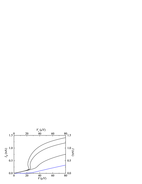
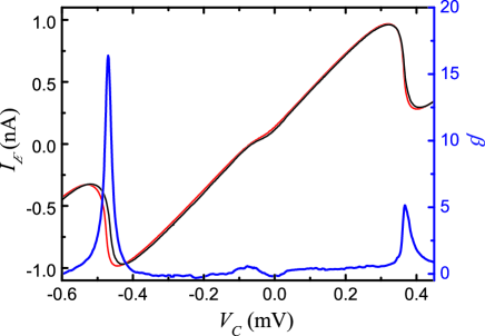
In the experiments on the Bloch Oscillating Transistor, we have also observed the Bloch nose and thus find the characteristic sign of Bloch oscillation. The curve of a Josephson junction in a resistive environment for sample 1 (see parameters in Table 1) is shown in Fig. 4. The curves are a result of a 2-point measurement where both the total current and the transformation are plotted against the total voltage and the junction voltage , respectively. In this way, one can truly see the Bloch nose in the form predicted in Refs. LZ ; Schon . The Bloch nose disappears when the ratio goes down, a manifestation of the fact that Zener tunneling sets in already at lower currents. Theoretically, the voltage for the onset of back bending is given by , when and the dissipation is due to quasiparticles in the JJ Schon . Without quasiparticle tunneling the blockade would become much larger, and for it would equal . In our experiment, the observed is 23 V, which is only little more than half of theoretical value: V.
The first report on the Coulomb blockade of Cooper pairs was made by Haviland et al. in Ref. haviland91 . Bloch oscillations and the role of Zener tunneling was investigated by Kuzmin et al. kuzmin94 ; kuzmin96 in experiments with a single Josephson junction in an environment of a chromium resistor. The characteristic Bloch nose feature, or the regions of negative differential resistance, was first measured for 1- and 2-dimensional SQUID arrays haviland2000 ; geerligs1989 . In later experiments using SQUID arrays as a tunable, but very nonlinear, high impedance environment, the Bloch nose could for the first time be clearly observed in a single Josephson junction watanabe2001 ; watanabe2003 . Although, there the authors plot vs. and do not make the transformation as done here. It should be noted, that our observation of the Bloch nose involves a real, linear resistive environment as the electromagnetic environment.
4.2 Device characteristics
4.2.1 DC Current-voltage characteristics
We will now describe the results of experiments of sample #1 ( parameters are given in Table 1, whereas for the definition of symbols, see Fig. 3) The maximum gain was achieved for the maximum ratio (0.3 for this sample). Hence, if not otherwise mentioned, all the following presentations of the results are given for this value. According to the theories on BOT operation outlined earlier, the gain should increase with . However, the theories assume that so that it suffices to consider only the dynamics between the first two bands. In the BOT measurements described in Ref. delahaye2 the maximum gain was achieved for , which also means that more than the two first bands may contribute to the dynamics.
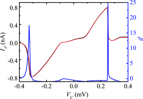
In Fig. 5 a typical -curve of the BOT is shown for two values of the base current and also the corresponding current gain is included in the graph. The BOT has current amplification for both positive and negative values of . However, as can be seen from the figure, the amplification is largest for negative . This we consider the ”normal operating mode” of the BOT and the gain region for positive we call the ”inverted mode”. Simulated curves and current gain are shown in Fig. 6 for the same device parameters as in the experiment. A slightly larger base current than in the experiment, 100 pA as compared to 40 pA, was used to find a matching current gain at the normal operating regime. The two sets of s’ look quite similar. However, the simulated one shows sharper features due to both a lower effective temperature and a higher base current, which leads to hysteretic behavior for the inverted operating region. Raising the temperature or lowering the base current in the simulation leads to a decreasing current gain. A prominent discrepancy between the experimental and simulated ’s is the location of the Bloch ”back bending” and the maximum gain. In the experiment, this region is about 100 V further than in the simulation. This is an indication of the fact that the dynamics may actually involve higher bands. More simulations for different BOT parameters can be found in Ref. hassel04 .
4.2.2 Current gain
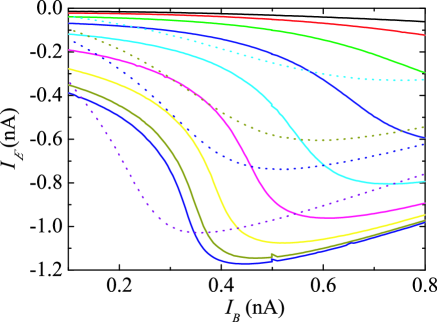
Next, we consider the relation for a fixed bias voltage and as a function of the ratio . In Figs. 7 and 8 the curves are shown for the normal and inverted operating regions. In these measurements, the extra collector resistance was absent, hence we have larger operating currents. In the simulated curves for the normal region, the gain was only about half of that which was observed experimentally, and the gain region is also much wider. However, by increasing the ratio in the simulation to values slightly above those obtained from the experiment (the simulated is included in Fig. 7), the simulated gains become closer to the experimental.
The simulation for the inverted mode showed diverging gains due to hysteretic behavior that leads to very low dynamic region (see also Fig. 10). This approach to hysteretic and divergent state could also be observed experimentally, as noticed in Fig. 8.
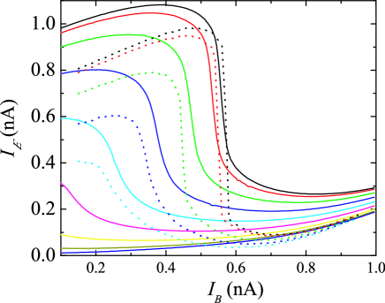
We measured the differential gain as a function of with lock-in amplifiers. The results for the normal operating region are presented in Fig. 9 for the case when the extra collector resistance was present. The gains are then a factor of 3 larger than in the above measurement without . This is also in close agreement to simulated gains, which will be discussed further in section 4.2.3.
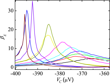
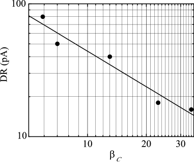
The dynamic region (DR) in terms of the base current can be inferred from the gain curves in Fig. 9 by using the relation: . The resulting DR versus plot is shown in Fig. 10. The large spread in the datapoints are mostly due to the errors in determining by numerical differentiation of curves. From the plot we see that the DR falls as (in fact, the exponent of the regression is ). As already mentioned, the simulated gains for the normal region had a much wider DR, though with less gain than in the experiment.
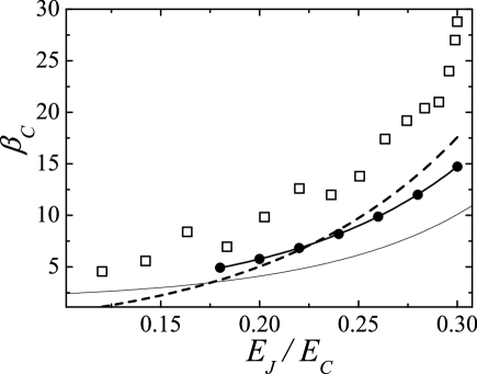
The analytic theory in Ref. hassel04 predicts that the gain should rise exponentially with the square of the ratio :
| (29) |
According to our simple model presented in Sec. the gain dependence is non-monotonic. This could, however, be a failure of the model as we are in a region were its validity is not guaranteed by the perturbation theory. For the gain starts to rise again. From the full time-dependent simulations, the dependence is also exponential but less than the normal mode gains from experiment (Fig. 11). When including heating effects in both the simulation and analytical model, decreased the gain and made the fit worse.
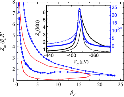
4.2.3 Input impedance
The applications of the BOT are largely determined by its input and output impedances, power gain and the noise temperature (for measurements on the noise temperature see lindell2005 ). We have studied the input impedance
| (30) |
at different levels of the current gain. In Fig. 12 the dependence is shown for the case where pA. The input impedance and were measured with lock-in amplifiers with excitation frequency of 17.5 Hz. The measurement results had to be corrected for the fact that part of the AC-current leaks through the stray capacitance, which mostly originates from the thermocoax. The corrected input impedance is then
| (31) |
where is the measured AC-differential impedance at the base and . With the assumption that pF, the AC and DC gains became equivalent.
The theoretical input impedance is easily calculated for the ”black box model” of Sec. 2.4, assuming lumped circuit elements and a known, constant current gain . Using the notation in Fig. 2 we can write for the island voltage
| (32) |
where , which includes the extra collector resistor. On the other hand we also have
| (33) |
As we know that we get from these two equations
| (34) |
and the input impedance is then
| (35) |
As is in our definition , the input impedance becomes positive. The input impedance observed in the experiment (Fig. 12) shows some deviation from the simple model. At the point of maximum gain the impedance is 1.4 the value of the model, but as one moves to either side of the maximum, the behavior is more complicated and also non-symmetric. The simulated curve reveals that the behavior could be anticipated from the dynamical model, which gives approximately the same 1.4 deviation from the simple model as observed in the experiment. The asymmetric feature shows that the simple model, that is proportional to , is followed quite closely for the part of the current gain where voltage is higher than the optimum operating point.
4.2.4 Power gain
An important measure of the device performance is the power gain
| (36) |
where and , and the currents are rms values. The simple black-box model for the input impedance, where , gives a theoretical power gain of
| (37) |
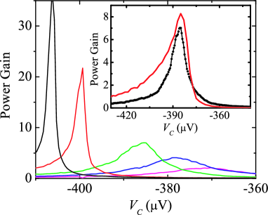
The setup for the power gain measurement is shown in Fig. 3. The AC-signal was capacitively coupled to by-pass the large bias resistor . We measured the power delivered by the BOT to a 100 k resistor (), which acted as a load at the collector. The measured power at the output is given by , where is the measured AC-voltage over the load. The measured power gain in this case becomes . The simple black box model gives a power gain of . Taking into account the measured input impedance in Fig. 12 we find that, for pA, , which agrees with the independent measurement in Fig. 13.
The power gains for pA at the normal operating point are shown in Fig. 13. The largest measured power gain was around 35 for pA. The output impedance of the device itself at the operating point was in the range k to k. The gain might be expected to grow rapidly when approaches . However, a positive load impedance with similar absolute magnitude as the negative output impedance may lead to oscillatory behavior.
A simulated power gain for pA is shown in the inset. The agreement looks fairly good but when the base current is increased in the simulation the effect on the gain is quite small compared to the large increase observed in the experiment. The simulation was also quite sensitive to the capacitance (see Fig. 3), here we settled for a ratio , which gave a good balance between achieving a more realistic model and simulation stability. The value of used in the simulation was 1 pF, which means that the base voltage drops less than 0.1 % when a quasiparticle tunnels to the island.
5 Conclusions
We have here briefly reviewed the physical principles and computational methods that have been applied to analyze the Bloch Oscillating Transistor. The circuit has been shown to produce a variety of interesting physical phenomena that also have a potential for practical applications. The measurements on the BOT have shown that the device works according to the physical principles discussed. The Bloch nose as a manifestation of the competition between coherent current via Bloch oscillations and Coulomb blockade of Cooper pairs was observed in a controlled resistive environment. The smallness of the observed blockade would indicate that the environmental dissipation is dominated by quasiparticles.
The optimal BOT parameters are quite difficult to specify, mainly, because the used models are approximations that hold in a certain regime for the parameters. We seek to optimize , , , and the capacitance , and at the same time keeping in mind what the optimum input and output impedances should be for a specific application. The analytic model of Sec 2.4 gives a closed formula for the current gain, and can thus used for optimization. In all the models, the gain grows with , but simultaneously, we have the requirement for the theories to be valid. However, nothing stops us to go to somewhat larger ratios in the simulation, although, the bands then increasingly deviate from the parabolic approximation. The simulation shows that the gains also increase with , but naturally, with the expense of the dynamic region. The simple analytic model does not depend on at all. However, in the analytical model of Ref. hassel04 the device performance improves as is reduced. A too transparent base junction would, however, be undesirable for many reasons: the increased transparency could increase charge fluctuations and destroy the Bloch oscillations in the Josephson junction. In fact, in our samples the NIS junction was quite resistive. Also, small would, in practice, mean larger capacitance and smaller blockade. The model indicates that a larger collector resistance is always desirable. This is probably a general conclusion, bearing in mind that the input impedance increases linearly with . In practice, fabricating chromium on-chip resistors larger than 0.5 M has proven difficult due to nonlinearities.
The observed device properties of the BOT can be qualitatively reproduced by simulations and the simple theoretical considerations presented here. There are, however, still quite many discrepancies between simulations and experiment. Often the values of the simulation for gains and impedances were a factor 2 from the experimental case. The simulations do show that the main operating principle of the BOT can be understood by the processes outlined. There are still some places for improvement, e.g., by taking into account the true phase fluctuations caused by tunneling of quasiparticles to the island. But, this would mean a great increase in the complexity of the simulation, introducing new numerical challenges. Also, taking into account the true band structure of the device might improve the agreement, especially for . While awaiting a more complete theoretical treatment, the simulations can be used for qualitative modelling of the BOT. The device could still be used as an on-chip amplifier and detector for mesoscopic experiments, where a good current gain is needed at medium level impedances, but, the exact device properties can be inferred only from experiment.
Acknowledgments
We acknowledge fruitful discussions with Julien Delahaye, Juha Hassel, Frank Hekking, Mikko Paalanen and Heikki Seppä. Financial support by Academy of Finland, TEKES and Centennial Foundation of Finnish Technology Industries is gratefully acknowledged.
Appendix
Transconductance
The transconductance can be calculated in the simple black box model by . For sample #1, S and the maximum observed transconductance was S.
For sample #2, which had a larger k, the transconductance was 9.1 S, which is about 3.5 larger than expected from the simple model above (see Fig. 14). The s cross at the dips in the -curves, thus giving rise to a sign change in transconductance, and also for the current gain. Thus, the input impedance stays positive in all measurements.
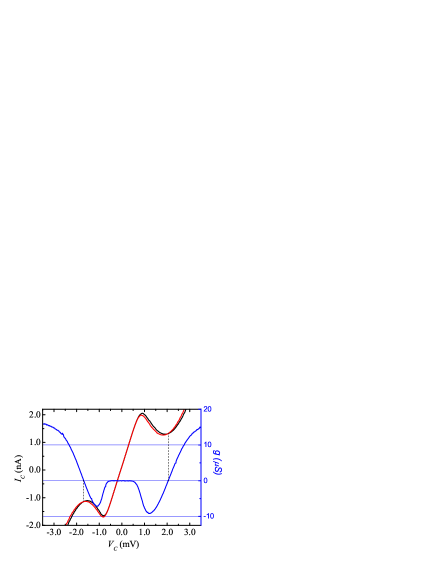
The curve for sample #2 was intrinsically hysteretic in behavior when applying a current bias to the base via an additional resistor at room-temperature. The hysteresis, however, disappeared when the biasing resistor was between 100 k and 1 M, which could indicate that the device has a region of negative input impedance in this range. Simulations have shown that the input impedance is always positive, but that the base curve can be hysteretic and, therefore, the observed hysteresis is a consequence of the device switching between two operating regimes, which have the same base current but different impedance levels.
References
- (1) See e. g. J. Clarke, A. N. Cleland, M. H. Devoret, D. Esteve and J. M. Martinis, Science 239, 992 (1988).
- (2) M. Tinkham, Introduction to Superconductivity, 2nd ed., McGraw-Hill, New York (1996).
- (3) D. B Haviland et al., Z. Phys. B 85, 339 (1991); L. S. Kuzmin and D. B Haviland, Phys. Rev. Lett. 67, 28920 (1991).
- (4) C. Kittel, Quantum Theory of Solids, John Wiley & Sons, New York (1963).
- (5) K. K. Likharev and A. B. Zorin, J. Low Temp. Phys. 59, 347 (1985); D. V. Averin, A. B. Zorin and K. K. Likharev, Sov. Phys. JETP 61, 407 (1985).
- (6) M. H. Devoret et al., Phys. Rev. Lett. 64, 1824 (1990).
- (7) T. Holst, D. Esteve, C. Urbina, and M. H. Devoret Phys. Rev. Lett. 73, 3455 (1994).
- (8) J. Delahaye, J. Hassel, R. Lindell, M. Sillanpää, M. Paalanen, H. Seppä, and P. Hakonen, Science 299, 1045 (2003).
- (9) J. Delahaye, J. Hassel, R. Lindell, M. Sillanpää, M. Paalanen, H. Seppä, and P. Hakonen, Phys. E 18, 15 (2003).
- (10) J. Hassel and H. Seppä, J. Delahaye and P. Hakonen, J. Appl. Phys. 95, 8059 (2004).
- (11) J. Hassel and H. Seppä, cond-mat/0404544; J. Hassel and H. Seppä, J. Appl. Phys. 97, 023904 (2005).
- (12) D. V. Averin and K. K. Likharev in Mesoscopic Phenomena in Solids (ed. by B. L. Altsuhler, P. A. Lee and R. A. Webb), Elsevier Science Publishers, Amsterdam (1991).
- (13) The quasicharge is analogous to the concept of crystal momentum. Hence, the real charge is always given by .
- (14) G. Schön and A. D. Zaikin, Phys. Rep. 198, 237 (1990).
- (15) R. J. Prance, H. Prance, T. P Spiller and T. D. Clark, Phys. Lett. A 166, 419 (1992).
- (16) D. J. Flees, S. Han and J. E. Lukens, Phys. Rev. Lett. 78, 4817 (1997).
- (17) R. Lindell, J. Penttilä, M. Sillanpää and P. Hakonen, Phys. Rev. B 68, 052506 (2003).
- (18) J. S. Penttilä, Ü. Parts, P. J. Hakonen, M. A. Paalanen and E. B. Sonin, Phys. Rev. Lett. 82, 1004 (1999).
- (19) C. Zener, Proc. R. Soc. A 145 523 (1934); E. Ben-Jacob, Y. Gefen, K. Mullen and Z. Schuss,Phys. Rev. B 37 7400 (1988); K. Mullen, Y. Gefen and E. Ben-Jacob, Physica B 152, 172 (1988); K. Mullen, E. Ben-Jacob and Z. Schuss, Phys. Rev. Lett. 60 1097 (1988).
- (20) D. V. Averin, Yu. V. Nazarov and A. A. Odintsov, Physica B 165&166, 945 (1990).
- (21) S. M. Girvin , L. I. Glazman and M. Jonson Phys. Rev. Lett. 64, 3183 (1990).
- (22) G. -L. Ingold and Yu. V. Nazarov, in Single Charge Tunneling (eds Grabert H. & Devoret M. H.) (Plenum Press, New York, 1992).
- (23) A. F. Andreev, Zh. Eksp. Teor. Fiz. 49, 655 (1965); Sov. Phys. JETP. 22, 455 (1966).
- (24) E. B. Sonin, Phys. Rev. B 70, 140506(R) (2004).
- (25) E. B. Sonin, PRL 98, 030601 (2007).
- (26) A. D Zaikin and D. S. Golubev Phys. Lett. A 164, 337 (1992).
- (27) R. K. Lindell and P. J. Hakonen, Appl. Phys. Lett. 86, 173507 (2005).
- (28) R. K. Lindell, J. Delahaye, M. A. Sillanpää, T. T. Heikkilä, E. B. Sonin, and P. J. Hakonen, Phys. Rev. Lett. 93, 197002 (2004).
- (29) M. Watanabe and D. B Haviland, Phys. Rev. Lett. 86, 5120 (2001).
- (30) M. Watanabe and D. B Haviland, Phys. Rev. B. 67, 094505 (2003).
- (31) L. S. Kuzmin, Y. Pashkin, A. Zorin and T. Claeson, Physica B 203, 376 (1994);
- (32) L. S. Kuzmin, Y. Pashkin, D. S. Golubev and A. Zorin, Phys. Rev. B 54, 10074 (1996).
- (33) D. B Haviland, K. Andersson and P. Ågren, J. Low Temp. Phys. 188, 733 (2000).
- (34) L. J. Geerligs, M. Peters, L. E. M. de Groot, A. Verbruggen and J. E. Mooij Phys. Rev. Lett. 63, 326 (1989).