High-quality quantum point contact in two-dimensional GaAs (311)A hole system
Abstract
We studied ballistic transport across a quantum point contact (QPC) defined in a high-quality, GaAs (311)A two-dimensional (2D) hole system using shallow etching and top-gating. The QPC conductance exhibits up to 11 quantized plateaus. The ballistic one-dimensional subbands are tuned by changing the lateral confinement and the Fermi energy of the holes in the QPC. We demonstrate that the positions of the plateaus (in gate-voltage), the source-drain data, and the negative magneto-resistance data can be understood in a simple model that takes into account the variation, with gate bias, of the hole density and the width of the QPC conducting channel.
pacs:
Valid PACS appear hereThe quantized plateaus observed in the conductance of a narrow constriction, the so-called quantum point contact (QPC), are the hallmarks of ballistic transport in a one-dimensional (1D) system vanWees88 ; Wharam88 . The QPC structure is also an essential building block for many other types of structures in mesoscopic physics, such as rings and quantum dots. Since the first observation of conductance quantization in QPCs based on GaAs/AlGaAs electrons vanWees88 ; Wharam88 , the quantization has been reported in electron systems in several other materials such as SiGe SiGe1 ; SiGe2 , GaN GaN , and AlAs AlAs . For a long time, there has also been interest in ballistic 1D transport in GaAs systems Zailer94 ; Daneshvar97 ; Rokhinson02 ; Danneau06 ; Koduv08 , partly because of the stronger spin-orbit interaction and the resulting spin-splitting of the energy bands at finite wavevectors Winkler03 . The realization of high-quality and stable QPCs in hole systems, however, has been challenging. Here we report on an exceptionally high-quality GaAs hole QPC device in which we observe up to 11 conductance steps and the “0.7” structure. We present a simple model that explains the gate-voltage dependance of the plateaus’ positions as well as the source drain bias data and the magneto-resistance of the QPC. Spacings between the quantized energy levels in this geometry are about 5 times larger than in previous reports of QPCs in other GaAs hole systems.
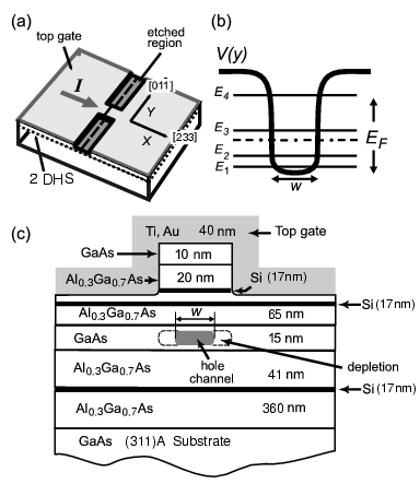
Our QPC device is based on a constriction made in a high-mobility, GaAs two-dimensional hole system (2DHS). The 2DHS is realized in a modulation-doped structure, grown on a GaAs (311)A substrate by molecular beam epitaxy. The 2DHS is confined to a GaAs quantum well flanked by un-doped (spacer) and Si-doped layers of Al0.3Ga0.7As. The top Al0.3Ga0.7As/GaAs interface is 112 nm below the surface. The layer sequence of the sample is schematically shown in Fig. 1(c) footnote1 . The 2DHS has a typical low-temperature mobility of cm2/Vs along the direction and cm2/Vs along at a 2D hole density of cm-2. The QPC is defined with a lithographic width of 300 nm and length of 400 nm. Figure 1(a) shows the sample geometry. The sample is etched 40 nm deep, using an electron cyclotron resonance plasma etcher with ZEP 520A resist as an etch mask, to fabricate a QPC with a strong confinement potential (Fig. 1b). A Ti/Au gate is then deposited on the top of the sample, covering the QPC channel as well as the adjacent 2DHS reservoirs. Applying a voltage bias, , to this gate changes the hole density in both the QPC channel and the reservoirs. We made measurements in a dilution refrigerator using the standard low-frequency AC lock-in techniques with an excitation of 10 V at 17 Hz.
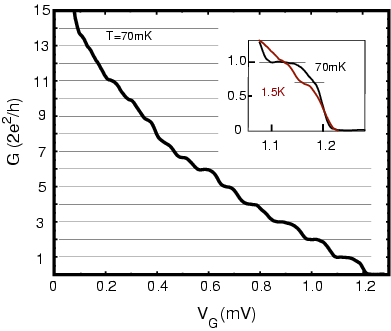
Figure 2 shows the conductance, , of the QPC device, measured at a temperature of = 70 mK as a function of . The QPC conductance exhibits 11 clear steps, most of which are well-quantized in multiple integers of . Note that in our structure, increasing leads to a narrowing of the constriction and also a lowering of the hole density in the 2D reservoirs and the QPC channel. As a result, the 1D hole subbands are depopulated one-by-one as is increased, and conductance plateaus are observed at , where is an integer denoting the number of occupied 1D subbands. The plateaus in our sample are quantized at the expected values for , except for = 7, 8, and 9. We do not know the origin of this anomaly, but we note that qualitatively similar anomalies have been observed in previous hole QPCs Rokhinson02 ; Koduv08 . In addition to the last non-zero plateau at , the device also shows the “0.7” structure which is more pronounced at higher temperatures as shown in the inset of Fig. 2.
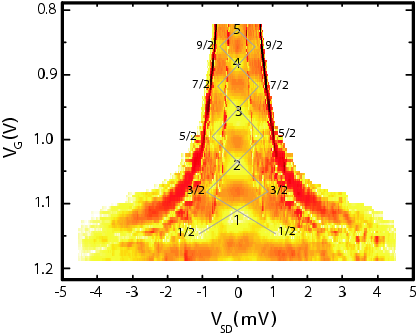
The separation between the 1D subband energies in a QPC channel can be extracted from measurements of the nonlinear conductance as a function of the source-drain bias, , applied across the QPC. In Fig. 3 we plot the differential transconductance of our device as a function of and the DC footnote2 . When is equal to the energy difference between the and subbands, an additional quantized conductance plateau with a value equal to an (2+1)/2 times appears. The subband energy spacing can then be deduced from the values at which these half-odd-integer plateaus are centered in Fig. 3. We find the energy spacings meV, meV, meV, and meV in our system. These are about 5 to 7 times larger than reported for other hole QPCs Danneau06 ; Koduv08 , likely because of the strong confinement potential in our device due to etching. Compared to the energy spacings in GaAs samples with similar, side-etched, QPC structures of Kristensen Kristensen00 , on the other hand, the spacings in our QPC are about 4 times smaller, qualitatively consistent with the much larger effective mass of holes compared to the electron effective mass.
Next, we describe a simple model for the potential landscape around the QPC, and compare its predictions to the experimental data. The model is similar to the one used by Gunawan AlAs to explain data for an AlAs electron QPC with a similar geometry, namely, a QPC which is side-etched and whose density is varied by biasing a top gate. Note that in our geometry (Fig. 1), as we decrease , increases and crosses the quantized energy levels in the QPC, leading to quantized conductance steps. We can deduce from the density () of the 2DHS reservoirs that surround the QPC; , in turn, can be determined from measurements of the Shubnikov-de Haas oscillations and the Hall resistance in the 2DHS reservoirs. Since the QPC confinement potential is strong and the quantized energies are small thanks to the large hole effective mass, we can estimate the 1D subband energy levels using an infinite square well model: , where is the hole effective mass and is the width of the (conducting) QPC channel. Assuming , where is the electron mass, we can then deduce the value of at the consecutive crossings of and . The width derived from this model is plotted in Fig. 4 as open circles. Now, it is also possible to estimate the channel width from the magneto-resistance of the QPC. When the QPC is subjected to a small perpendicular magnetic field, its resistance exhibits a strong negative magneto-resistance which ends with a pronounced kink at a characteristic field , marking the field at which the classical cyclotron diameter equals the channel width AlAs ; kink ; kink2 . Using one can then estimate the width of the QPC: , where is the Fermi wavevector. The filled diamonds in Fig. 4 show the width deduced from the kink positions in the magneto-resistance data for our sample; the error bars represent the uncertainty in determining the kink positions. Note that we have ignored the complications in hole bands arising from the spin-orbit interaction, i.e., we assumed that the holes in the QPC are spin degenerate and have a circular Fermi contour. Despite these simplifications, the channel widths deduced from two independent sets of data, namely the positions of the conductance plateaus and the field positions of the magneto-resistance kinks, are in good agreement.
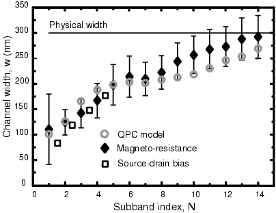
The source-drain bias data provide a third, independent measure of : The energy level spacing in the QPC is . Open squares in Fig. 4 represent deduced from source-drain data and are plotted vs. the average of each two consecutive . These width are also in agreement with determined from the other two techniques. It is also noteworthy that the deduced are smaller than the physical (lithographical) width of the QPC and decrease with decreasing subband index; this behavior is reasonable, as we expect that the depletion areas near the QPC channel grow as the hole density is lowered AlAs .
Our work was supported by the NSF MRSEC and DOE. We thank B. H. McGuyer for help with the measurements.
References
- (1) B. J. van Wees, H. van Houten, C. W. J. Beenakker, J. G. Williamson, L. P. Kouwenhoven, D. van der Marel, and C. T. Foxon, Phys. Rev. Lett. 60, 848 (1988).
- (2) D. A. Wharam, T. J. Thornton, R. Newbury, M. Pepper, H. Ahmed, J. E. F. Frost, D. G. Hasko, D. C. Peacock, D. A. Ritchie and G. A. C. Jones, J. Phys. C 21, L209 (1988).
- (3) D. Tobben, D. A. Wharam, G. Abstreiter, J. P. Kotthaus, and F. Schaffler, Semicond. Sci. Technol. 10, 711 (1995).
- (4) U. Wieser, U. Kunze, K. Ismail, and J. O. Chu, Appl. Phys. Lett. 81, 1726 (2002).
- (5) H. T. Chou, S. Luscher, D. Goldhaber-Gordon, M. J. Manfra, A. M. Sergent, K. W. West, and R. J. Molnar, Appl. Phys. Lett. 86, 73108 (2005).
- (6) O. Gunawan, B. Habib, E. P. De Poortere, and M. Shayegan, Phys. Rev. B 74, 155436 (2006).
- (7) I. Zailer, J. E. F. Frost, C. J. B. Ford, M. Pepper, M. Y. Simmons, D. A. Ritchie, J. T. Nicholls, and G. A. C. Jones, Phys. Rev. B 49, 5101 (1994).
- (8) A. J. Daneshvar, C. J. B. Ford, A. R. Hamilton, M. Y. Simmons, M. Pepper, and D. A. Ritchie, Phys. Rev. B 55, R13409 (1997).
- (9) L.P. Rokhinson, D. C. Tsui, L. N. Pfeiffer, and K. W. West, superlattices Microstruct. 32, 99 (2002).
- (10) R. Danneau, W. R. Clarke, O. Klochan, A. P. Micolich, A. R. Hamilton, M. Y. Simmons, M. Pepper, and D. A. Ritchie, Appl. Phys. Lett. 88, 12107 (2006).
- (11) S. P. Koduvayur, L. P. Rokhinson, D. C. Tsui, L. N. Pfeiffer, and K. W. West, Phys. Rev. Lett. 100, 126401 (2008).
- (12) R. Winkler, Spin-Orbit Coupling Effects in Two-Dimensional Electron and Hole Systems, (Springer, Berlin, 2003).
- (13) The 17 nm-thick Si-doping layers on the sides of the 15 nm GaAs quantum well have a Si densitiy of cm-3 and the top doping layer has a Si density of cm-3.
- (14) The data in Fig. 3 have been corrected for the voltage drop across the series resistance of the cryostat filtered wires.
- (15) A. Kristensen, H. Bruus, A. E. Hansen, J. B. Jensen, P. E. Lindelof, C. J. Marckmann, J. Ngård, C. B. Sørensen, F. Beuscher, A. Frochel, and M. Michel, Phys. Rev. B 62, 10950 (2000).
- (16) H. van Houten, C. W. J. Beenakker, P. H. M. van Loosdrecht, T. J. Thornton, H. Ahmed, M. Pepper, C. T. Foxon, and J. J. Haris, Phys. Rev. B 37, 8534 (1988).
- (17) K. F. Berggren, T. J. Thornton, D. J. Newson, and M. Pepper, Phys. Rev. Lett. 57, 1769 (1986).