Contact conductance between graphene and quantum wires
Abstract
The contact conductance between graphene and two quantum wires which serve as the leads to connect graphene and electron reservoirs is theoretically studied. Our investigation indicates that the contact conductance depends sensitively on the graphene-lead coupling configuration. When each quantum wire couples solely to one carbon atom, the contact conductance vanishes at the Dirac point if the two carbon atoms coupling to the two leads belong to the same sublattice of graphene. We find that such a feature arises from the chirality of the Dirac electron in graphene. Such a chirality associated with conductance zero disappears when a quantum wire couples to multiple carbon atoms. The general result irrelevant to the coupling configuration is that the contact conductance decays rapidly with the increase of the distance between the two leads. In addition, in the weak graphene-lead coupling limit, when the distance between the two leads is much larger than the size of the graphene-lead contact areas and the incident electron energy is close to the Dirac point, the contact conductance is proportional to the square of the product of the two graphene-lead contact areas, and inversely proportional to the square of the distance between the two leads.
pacs:
81.05.Uw, 73.63.Rt, 73.23.-b, 72.10.-d1. Introduction
The fabrication of graphene, a single atomic layer of graphite, is the first experimental realization of realistic two-dimensional crystal refNovoselov1 . In the effective mass approximation, valence electrons in such a carbon material obey the massless relativistic Dirac equation, rather than the Schrödinger equation. Consequently, graphene presents many unusual electronic transport properties, such as the half-integer quantum Hall effect refzheng ; refGusynin ; refYb.Zhang ; refNovoselov ; refPeres , the nonzero conductivity minimum at vanishing carrier concentration refNovoselov ; refM.I.Katsnelson1 ; refJ.Tworzydlo ; refAKGeim ; refFMiao ; refYW.Tan ; refK.Ziegler ; refK.Ziegler2 , the subtle weak localization refSuzuura ; refS.V.Morozov ; refA.F.Morpurgo ; refKhveshchenko ; refE.McCann ; refXiaosongWu , and the reflectionless transmission of the carrier through an arbitrarily high barrier refKrekora ; refM.I.Katsnelson ; refV.V.Cheianov .
The intriguing transport properties mentioned above are closely associated with the scattering of a Dirac electron by impurities, defects or gated barriers, etc. However, apart from these scattering effects, the contact between graphene and the metallic electrodes also influences the electronic transport spectrum to some extent. In other words, the measured conductance(conductivity) spectrum often includes a contact conductance, accompanying the scattering conductance. From the experimental viewpoint, such a contact conductance makes sense when graphene couples to the probes of the scanning tunneling microscope (STM) refKobayashi ; refNiimi ; refH.Amara , or ultrathin gold or tungsten wires; in particular, the multi-probe STM that was developed quite recently refJ.Onoe ; refK.Takami ; refO.Guise ; refM.Ishikawa ; refO.Kubo , which can be used to explore the surface structure of graphene. In these actual structures, the leads that connect graphene and electron reservoirs are the quantum wires which have only a few transverse modes to carry the current. This is in contrast with the infinitely many transverse modes in graphene. Thus, the electron will be reflected with certain probability when it enters the leads from graphene. Besides, such quantum wires couple locally to a finite number of the carbon atoms of graphene. As a result, the electronic tunneling between the leads and graphene depends sensitively on the coupling configuration at the contact. To sum up these facts, it can be anticipated that the coupling between graphene and a quantum wire will give a nontrivial contact conductance.
So far, relatively fewer works involve the contact conductance between graphene and the leads of different kinds refYMBlanter ; refSchomerus , in comparison with the scattering conductance. In fact, many aspects concerning this issue deserve further explorations. In the present work, we carry out a systematic investigation on the contact conductance between graphene and quantum wires which serve as the leads to conduct the current. There are many factors that influence the contact conductance, for example, the bandwidth and the band position of the quantum wire(lead) relative to the Dirac point of graphene, the coupling configuration between the leads and graphene, and the distance and the relative orientation between the two leads. To obtain a quantitative dependence of the contact conductance on these factors it is desirable to analyse the observed conductance spectrum in relevant experimental setups.
The rest of this paper is organized as follows: In Sec.2, the theoretical framework to formulate the contact conductance is elucidated. In Sec.3, the numerical calculations on the contact conductance are performed. Based on these numerical results, the dependence of the contact conductance on the relevant parameters is discussed. Finally, in Sec.4, we make some concluding remarks.
2. Model and theory
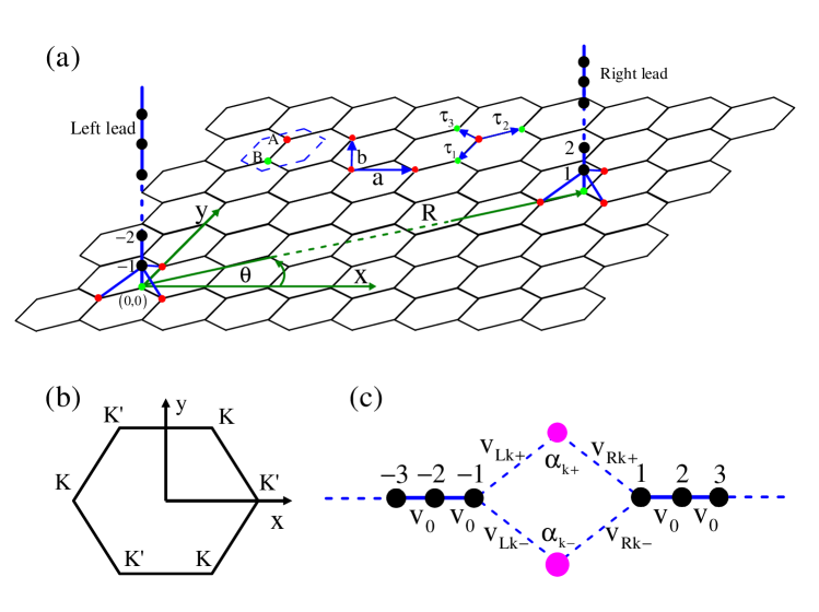
As illustrated in Fig.1, the electronic transport structure we consider consists of a graphene monolayer coupling to two quantum wires, which serve as two leads to conduct the current. We adopt a semi-infinite linear lattice to describe the band structure of a single transverse mode in each lead. Such a single mode lead couples to the finite number of the carbon atoms in graphene. Note: Some structure parameters are explained in Fig.1.
In such a model the tight-binding Hamiltonian of an electron is composed of three parts,
| (1) |
The first term is the Hamiltonian of the two semi-infinite linear lattices which model the two leads. It is given by
| (2) |
where () is the electron creation (annihilation) operator at the individual lattice points. For the ideal leads, both the on-site energy and the hopping energy are viewed as uniform parameters, denoted by and , respectively. The second term is the tight-binding Hamiltonian of the band electron in graphene. It takes a form as
| (3) |
where with or B is the electron creation(annihilation) operator associated with the local atomic orbits in graphene. The notation means that the summation is restricted between the pairs of the nearest neighbor carbon atoms. is the corresponding hopping energy. We choose the Dirac point as the energy reference point, hence the on-site energy of all lattice points in graphene is zero. Moreover, in what follows we use the units . The last term in the total Hamiltonian describes the electron tunneling between the leads and graphene. It is given by
| (4) |
where and denote the coupling strength between two leads and the individual carbon atoms in graphene. Note that we use L and R to denote the two leads respectively. As illustrated in Fig.1, only finite carbon atoms around the tip of each lead couple to the lead effectively.
To study the electronic transport properties, we need to calculate the linear conductance between the two leads. Based on the Landauer-Büttiker theory refLandauer ; refM.Buttiker , we can write the linear conductance formula as
| (5) |
where is the energy of the incident electron from one lead. The matrices of the retarded and advanced Green functions satisfy a relationship . The matrix element is given by and , just following the standard definition of a retarded Green function. We will often use an alternative notation to denote the retarded Green function in Fourier space for convenience, e.g. . In Eq.(5) two other matrices are defined as and , where the subscript “0” denotes that the corresponding Green function belongs to an individual lead, completely isolated from graphene. Besides, as we have done, we will often drop the energy dependence of these matrices to keep expressions compact.
To solve the Green functions in the conductance formula, we need to convert the Hamiltonian into the eigen-representation of the band electron of graphene. Doing so, we utilize the following transformations
| (6) |
and
| (7) |
where is the total number of unit cells in graphene; with being the electron wave vector measured from the center of the Brillouin zone of graphene. The creation (annihilation) operator () is associated with electron Bloch state in one sublattice of graphene. And the notation or , denotes the conduction or valence bands of graphene, respectively. is the creation (annihilation) operator of the eigen-states of the valence electron in graphene. Thus, the Hamiltonian of graphene becomes diagonal
| (8) |
where . Accompanying such a representation transformation, the tunneling Hamiltonian can be rewritten as
| (9) |
with
| (10) |
Meanwhile, the conductance expression changes into
| (11) |
The retarded Green function satisfies the following equation of motion
| (12) | |||||
where and with being a positive infinitesimal. Here, we can see that the Green functions are the relevant quantities to calculate the linear conductance, which are exactly solvable. Taking as an example, the set of the equation-of-motion with regard to this Green function consists of
| (13) |
and
| (14) |
In the above equations
| (15) |
By virtue of the property of a tri-diagonal matrix refKuo , we can solve analytically the above set of equations, which yields
| (16) |
with
| (17) |
and
| (18) |
In similar manner, we can obtain the analytical forms of Green functions , and . They are given by
| (19) |
| (20) |
and
| (21) |
Substituting these results into Eq.(12), we can then get the explicit form of the Green function . Subsequently, after some derivation, we obtain an analytical expression for the contact conductance. That is
| (22) |
| (23) |
with
| (24) |
and
| (25) |
So far we have obtained a conductance expression in terms of the self-energy terms . We will derive their the analytical forms in the Appendix. To calculate the conductance spectrum, the two parameters and ought to be taken the appropriate values to guarantee the energy band of the leads and the linear region of the band of graphene overlaps each other. Besides, the incident electron energy should also be restricted in the linear region of graphene band. Now we consider an extreme case that the graphene-lead coupling is far much smaller than the bandwidth of the leads, i.e. . From the above conductance expression, we can infer that the conductance formula in such a weak coupling limit reduces to
| (26) |
3. Results and discussion
After formulating the linear conductance, we are now in a position to perform the numerical calculation for the conductance spectrum, from which we can investigate the electronic transport properties dominated by the contacts between graphene and two quantum wires.
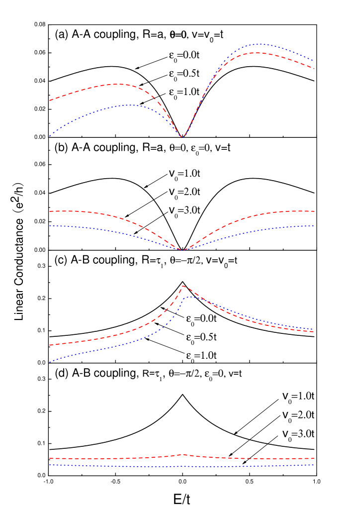
First of all, we consider the simplest case that only one carbon atom in graphene couples to each lead(Hereafter we call the tip of a lead a probe). For the numerical calculation, we fix the first probe(L) to couple to the atom at origin, and shift the second probe around. In Fig.2, we show the calculated contact conductance spectrum ( versus ) for the second probe(R) stopping at a specific A atom. In such a case we have and . We refer to such a configuration between graphene and two leads as A-A coupling. The most striking feature shown in this figure is that the contact conductance vanishes when the incident electron energy is aligned with the Dirac point of graphene. From the analytical results given in the Appendix, we can readily obtain the self-energy terms for the case of the simple A-A coupling
| (27) |
| (28) |
Owing to the chirality of the band electron in graphene, these self-energies vanish at Dirac point(). Then, this leads to the zero point of the contact conductance as shown in Fig.2. Therefore, we can attribute the zero contact conductance at the Dirac point to the chirality of the Dirac electron. As shown in Fig.2(a), we can shift the position of the band bottom of the leads relative to the Dirac point by varying the parameter . As a result, the conductance spectrum becomes asymmetric with respect to the Dirac point. In addition, Fig.2(c) shows that when the band of the leads is widened by increasing the parameter , the conductance becomes notably smaller. Such a dependence of the contact conductance spectrum on the band structure of the leads can be readily understood by analyzing the local density of states of the electron at the tip of a lead, which appears in the conductance formula, see Eqs.(22), (23) and (26). From Eq.(25) we can see that such a local density of states decreases as the bandwidth of a lead gets larger. Besides, when the parameter deviates from the Dirac point, the local density of states becomes asymmetric relative to the Dirac point. The variation of the conductance spectra with the parameters and shown in Fig.2(a) and (b) just reflects these features of the local density of states. In Fig.2(c) and (d) we show the contact conductance spectrum for the so-called A-B coupling which means that the second probe couples solely to a atom at a specific position. In such a case the band structure of the leads influences the conductance spectrum in the same way as the case of A-A coupling, namely, the conductance spectrum becomes asymmetric with the shift of and decreases globally with the increase of . However, for the case of A-B coupling a conductance peak occurs at Dirac point in place of the conductance zero in A-A coupling. This is due to that the self-energy for A-B coupling takes a different form. It is given by
| (29) |
By a simple derivation, we can further deduce that for the A-B coupling the self energies at the Dirac point are and
| (30) |
Then the contact conductance at the Dirac point takes a simple form as
| (31) |
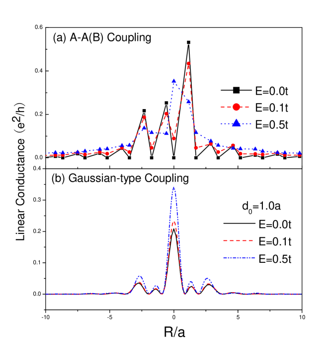
With the help of these self-energy terms we can discuss the dependence of the contact conductance on the distance between the two probes. In fact, from Eqs.(29)-(31) we can infer that initially with the increase of the distance between the two probes, the contact conductance near the Dirac point will decay rapidly. However, when the distance between the two probes becomes sufficiently large, the contact conductance tends to be inversely proportional to . In Fig.3(a) we plot the contact conductance as a function of by letting the second probe to move away from the origin (the position of the first probe) along the y axis. We can see that the contact conductance decreases drastically when increases within several times the lattice constant. Such a rapid decay has little to do with the variation of the incident electron energy.
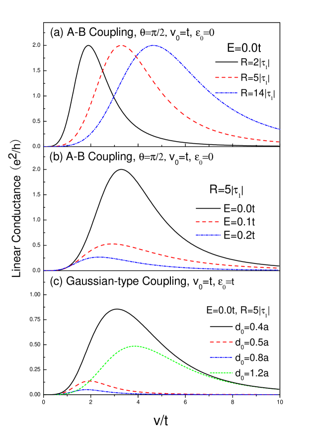
The explicit expression of the contact conductance at the Dirac point shown by Eq.(31) indicates a conductance peak occurs when . This implies that the resonance will occur when the distance between the two probes takes an appropriate value, which depends on the bandwidths of the leads and their coupling strengths to graphene. To study such a resonance in some details, we calculate the conductance as a function of the strength of the graphene-lead coupling, as shown in Fig.4. From Fig.4(a) we can see that a stronger graphene-lead coupling is required to observe resonance when the distance between the two probes gets larger. The calculated results shown in Fig.4(b) indicate that the resonant conductance peak is notably suppressed when the incident electron energy deviates from the Dirac point.
Now we turn to discuss the orientation dependence of the linear conductance when the second probe shifts around the origin where the first probe is located. For simplicity, we only consider the weak graphene-lead coupling limit, where the conductance expression takes a relatively simple form, given by Eq.(26). From Eqs.(28) and (29) we can see that the factors for A-A coupling and for A-B coupling determine the orientation dependence of the linear conductance. Our derivation in the Appendix indicates that such orientation factors originate from quantum interference between the K and K’ valleys. Consequently, when the length of (the distance between the two probes) is fixed, the maximum of the conductance appears when is along direction. Furthermore, considering the symmetry of the honeycomb lattice of graphene, when the second probe moves along a circle around the first probe, the conductance maximum will appear at the directions. In addition, we can readily infer that for A-A coupling the conductance pattern formed by shifting the second probe has reflection symmetry with respect to the x axis. In other words, when the second probe is located at the two symmetric A atoms relative to the x axis, the conductance gives the same value.
The above coupling manner that a quantum wire couples to a single carbon atom in graphene can only model the extreme situation that the probe aims at a specific carbon atom, but the coupling strength between the probe and the adjacent carbon atoms is negligibly small. To mimic the actual graphene-lead coupling configuration, we introduce the following Gaussian-type graphene-lead coupling
| (32) |
where denotes the arbitrary position of probe , and is the lattice vector of a carbon atom in the vicinity of the probe. is a decaying factor to determine the region in which the carbon atoms couple effectively to the probe. Obviously, when is far smaller than the lattice constant, such a Gaussian-type coupling changes into the single atom coupling configuration discussed above. On the other hand, when is comparable to or larger than the lattice constant, a probe will couple to multiple carbon atoms around it.
At first, we check whether the contact conductance vanishes at the Dirac point when the two probes are positioned at two carbon atoms of the same kind. As shown in Fig.3(b), we can see that such a chirality associated feature no longer exists when the effective coupling region gets larger. This is readily understood since in the Gaussian-type coupling configuration with a decay factor comparable to the lattice constant of graphene, the conductance is the averaging result of A-A and A-B couplings. Besides, the result shown in Fig.3(b) indicates that the rapid decay of the contact conductance with the increase of the probe interval still holds in such a Gaussian-type graphene-lead coupling. In Fig.4(c) we show the resonant contact conductance by changing the strength of the graphene-lead coupling in Gaussian type. We can infer that the resonant conductance peak is influenced by the decay factor intricately. Initially when we increase the decay factor( to 0.8) there is a notable decrease in the resonant peak. But when we increase further, the conductance peak turns to get larger. Such a complicated dependence of the conductance on the effective coupling size arises from the quantum interference between the different electron transmission paths. When an electron travels from the first probe to the second one, electronic tunnelings between graphene and the two probes can be realized via two carbon atoms of either the same kind or the distinct kind, which corresponds to the different electron transmission paths. These two distinct electron transmission paths result in destructive interference. At , besides the central B atom, three nearest neighbor A atoms begin to couple effectively to the second probe. As a result, the destructive quantum interference diminishes the resonant peak. When , six next-nearest neighbor B atoms enter the effective region to couple to the second probe, which compensate for the negative effect of the three nearest neighbor A atoms. As a result, there is a notable increase in the resonant peak.
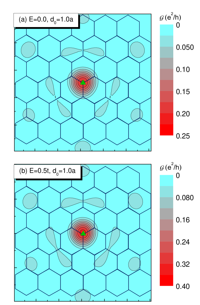
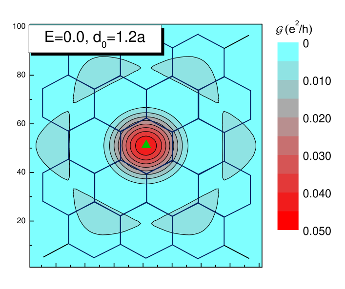
With such a Gaussian-type coupling manner we can plot the two-dimensional conductance pattern formed by shifting the second probe around the first one. In Fig.5 we plot such a conductance pattern for a relatively small decay factor in the Gaussian-type coupling function(). This case is in analogy to the single atom coupling configuration discussed above. From this figure we can see that the conductance pattern exhibits the group symmetry when the second probe rotates around the first probe. And such a rotation symmetry is independent of the incident electron energy. The strongest conductance appears when the second probe is located at the next-nearest neighbor B atoms, rather than the three nearest neighbor B atoms around the origin (Except for the conductance maximum at the origin when the incident electron energy is far away from the Dirac point, as shown in Fig.5(b)). According to the discussion on the relation between the resonant conductance peak and the probe interval, the strongest conductance can appear at different positions if we adjust the coupling strength between the probes and graphene. In Fig.6 we plot the conductance pattern corresponding to a relatively large decay factor(). We can see that the group symmetry remains in this conductance pattern. And conductance pattern does not vary notably with the variation of the incident electron energy. Unlike the case of where the conductance maxima always occur when the second probe points at an individual carbon atom, some discrete islands with different shapes form in Fig.6, labeling the regions with the relatively large conductance. As shown in Fig.7, if we move the first probe to the center of a hexagon of the graphene lattice, the conductance pattern formed by shifting the second probe around has the group symmetry instead of the group symmetry in the previous cases shown in Fig.5 and Fig.6. However, in such a case the conductance is far smaller than those in the previous cases. This is because that the first probe does not point at any atom carbon. Thus, according to the Gaussian-type coupling function, the coupling strength between the carbon atoms in graphene and this lead diminishes notably.
Finally, based on the above discussion, we can work out an approximate expression for the contact conductance, which is convenient for a rapid estimation of the contact conductance for some experimental setups if the following conditions are satisfied. First, if the distance between the two probes, symbolized by , is much larger than the size of the effective contact area around each probe, thus to calculate the self-energies from the formulae given in the Appendix, we can replace the exact distance between two individual carbon atoms around two probes by approximately. Second, when the incident electron energy is limited in the vicinity of the Dirac point, we can roughly view . Thus, according to the formulae shown in the Appendix, the dominant contribution to the self-energy arises from and . Consequently, we arrive at an approximate expression about the contact conductance in the weak coupling limit, which is given by
| (33) |
where denotes the number of the same kind in graphene which couple effectively to probe . Obviously, such a quantity is proportional to the contact area between graphene and the probe. If the probe interval is much larger than the lattice constance of graphene, we will have
| (34) |
where is the argument of . Therefore, we can conclude that the contact conductance is proportional to the square of the two contact areas between graphene and the two probes, and inversely proportional to the square of the probe interval, if the conditions given above are satisfied.
4. Conclusions
In this work we have systematically studied the contact conductance between graphene and two quantum wires which serve as the leads to connect electron reservoirs and graphene. The general conclusion we have obtained is that the contact conductance decays rapidly with the increase of the distance between the two leads. When each quantum wire couples to only one carbon atom in graphene, the contact conductance vanishes at the Dirac point if the two carbon atoms coupling respectively to the two leads belong to the same sublattice of graphene. And this conductance zero arises from the chirality of the Dirac electron in graphene. Also at the Dirac point, if two quantum wires couple to two carbon atoms of distinct kinds, a resonant path can be formed by adjusting the strength of the graphene-lead coupling. The inter-valley quantum interference causes the orientation dependence of the contact conductance. In the weak graphene-lead coupling limit, the carbon-carbon bond directions(i.e. directions) are the optimal directions to form the maximal contact conductance. In a more realistic situation, each quantum wire may couple effectively to multiple carbon atoms around it. To mimic such a situation, we introduce Gaussian-type graphene-lead coupling, by which we have worked out the two-dimensional conductance pattern formed by moving the second probe around the first one. We find that the conductance pattern does not vary sensitively with the incident electron energy. However, the symmetry of the conductance pattern changes from group to group when the first probe shifts from a carbon atom to the center of a hexagon of the graphene lattice. Finally, we obtain an approximative expression about the contact conductance when the probe interval is sufficiently large and the incident electron energy is in the vicinity of the Dirac point. We find that in such a case the contact conductance is proportional to the square of the two contact areas between graphene and the probes, and inversely proportional to the square of the probe interval.
Acknowledgements
This work was financially supported by the National Natural Science Foundation of China under Grant NNSFC10774055.
Appendix
Now we derive the explicit expression about the self-energy terms in terms of the structure parameters. Substituting Eq.(10) into Eq.(15) we have
| (35) |
In the above we have introduced four auxiliary functions which can be analytically treated by invoking the linear dispersion relation of graphene around the Dirac point.
| (36) | |||
| (37) |
| (38) |
and
| (39) |
where is the so-called Fermi velocity and
| (40) |
It should be noticed that in Eq.(37) the incident electron energy appears in the analytical result of the functions and as a prefactor. It arises from the chirality of the Dirac electron in graphene. This result implies that these two functions are equal to zero when the incident electron energy is aligned with the Dirac point. Besides, our derivation indicates that the quantum interference between K and K’ valleys in the band structure of graphene is responsible for the dependence of the four functions given above, hence the contact conductance, on the relative orientation between the two probes.
References
- (1)
- (2)
References
