Charge state of the O2 molecule during silicon oxidation through hybrid functional calculations
Abstract
We study the charge state of the diffusing O2 molecule during silicon oxidation through hybrid functional calculations. We calculate charge transition levels of O2 in bulk SiO2 and use theoretical band offsets to align these levels with respect to the Si band edges. To overcome the band-gap problem of semilocal density fuctionals, we employ hybrid functionals with both predefined and empirically adjusted mixing coefficients. We find that the charge transition level in bulk SiO2 occurs at 1.1 eV above the silicon conduction band edge, implying that the O2 molecule diffuses through the oxide in the neutral charge state. While interfacial effects concur to lower the charge transition level, our estimates suggest that the neutral charge state persists until silicon oxidation.
pacs:
71.55.-i, 71.15.Mb, 73.40.QvDetermining the nature and origin of point defects at semiconductor-oxide interfaces is a major step in the development of electronic devices.Sze Since direct experimental characterization of interfaces is often difficult, simulation methods based on density functional theory (DFT) are increasingly being used as an alternative tool for the investigation of atomic-scale properties. However, the study of defect levels within standard DFT schemes is still largely hindered by the well-known band-gap problem. Indeed, calculated band gaps and band offsets are generally severely underestimated and the alignment of defect levels with respect to the relevant band edges is consequently affected. A correct alignment is a prerequisite for understanding issues such as oxide charging,Robertson_RPP_2006 defect passivation, Fermi-level pinning,Broqvist_APL_2008 stress-induced leakage current,Bloechl_PRL_1999 charge state of defects, etc.
Silicon oxidation is a fundamental process in which charging issues are expected to play a key role.Sofield_SST_1995 Our understanding of this process relies to a large extent on the model proposed by Deal and Grove, in which oxide growth proceeds through the diffusion of the oxygen molecule across the oxide followed by its incorporation at the silicon substrate.Deal_JAP_1965 While supporting this general picture, DFT calculations have been instrumental to achieve an atomic scale description of various aspects of silicon oxidation, such as the diffusion mechanism, Bongiorno_PRL_2002 ; Bakos_PRL_2002 the oxidation reaction, Bongiorno_PRL_2004 ; Orellana_PRL_2001 the role of spin, Kato_PRL_1998 the layer-by-layer oxidation, Watanabe_PRL_1998 ; Tsetseris_PRL_2006 and the release of interstitial silicon.Kageshima_PRL_1998 However, the charge state of the O2 molecule during the oxidation process has so far remained elusive. This is expected to determine the nature of the oxygen species occurring at the interfaceStoneham_PRB_2001 and consequently the oxidation reaction and the atomic structure at the Si-SiO2 interface.Sofield_SST_1995 ; Bongiorno_PRL_2004 ; Stoneham_PM_1987
Experimental attempts to determine the charge state of the oxidizing molecule rest on the study of the oxide growth kinetics in applied electric fields, but result in conflicting conclusions.Jorgensen_JCP_1962 It should further be noted that the interpretation of such measurements is not trivial because of the complexity of the underlying atomic processes.Bongiorno_PRL_2002 Theoretical work based on gradient corrected DFT calculations concluded that the oxygen molecule diffuses through the oxide in a metastable neutral charge state, assuming the stable negatively charged state only in the vicinity of the substrate where electron tunneling can occur.Stoneham_PRB_2001 This leads to a description of silicon oxidation in which neutral and negatively charged oxygen species play competing roles.Stoneham_PRB_2001 This inference directly stems from the position of the charging level of the O2 molecule relative to the silicon band edges. However, the theoretical determination of such an alignment is subject to the band-gap problem.
In this work, we determine the charge state of the O2 molecule during silicon oxidation by locating its charge transition level with respect to the relevant band edges at the Si-SiO2 interface. To overcome the band-gap problem, we use hybrid density functionals which give enhanced band gaps compared to semilocal functionals.Muscat_CPL_2001 Our results indicate that the neutral state of the oxygen molecule is thermodynamically most stable in bulk SiO2 for electron chemical potentials lying in the Si band gap. In the vicinity of the substrate, the image-charge interactions and the higher oxide density concur to lower the charge transition level. Nevertheless, our estimates of their effects suggest that the O2 molecules preserve their neutral state until the onset of oxidation.
We considered the class of hybrid density functionals based on the generalized gradient approximation of Perdew, Burke, and Ernzerhof (PBE),PBE which are obtained by replacing a fraction of PBE exchange with Hartree-Fock exchange. The functional defined by = is referred to as PBE0 and has received some support from theoretical considerations.PBE0 In our calculations, core-valence interactions were described through normconserving pseudopotentials and valence wave functions were expanded in a plane-wave basis set. The basis set is defined by an energy cutoff of 70 Ry. The pseudopotentials were generated at the PBE level and used in all calculations. The electronic-structure calculations corresponding to large supercells were performed with a Brillouin-zone sampling restricted to the point. For bulk silicon, we determined the band edges using a converged -point sampling. The integrable divergence of the Hartree-Fock exchange term was explicitly treated.Gygi_PRB_1986 Structural relaxations were carried out at the PBE level. We used the quantum-espressoQE and cpmdCPMD codes.
For the Si-SiO2 interface, we used a superlattice structure, in which a crystalline Si layer (9 monolayers) and an amorphous SiO2 layer (17 Å) are periodically repeated.Giustino_PRL_2005 The interface structure was designed to incorporate a set of atomic-scale features inferred from experimental data.Bongiorno_PRL_2003 The simulation cell in the transverse directions corresponds to a Si(100) interface unit. The model contains 131 Si atoms and 86 O atoms. For bulk amorphous SiO2, we used a disordered 72-atom model structure obtained previously.Sarnthein_PRB_1995
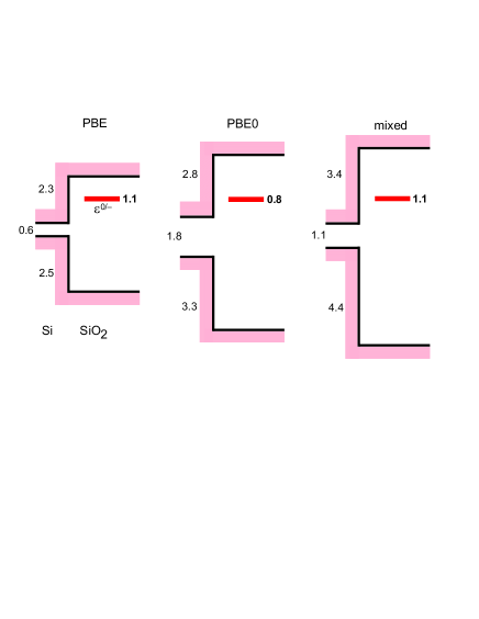
| PBE | 0.6 | 5.4 | 2.5 | 2.3 |
|---|---|---|---|---|
| PBE0 | 1.8 | 7.9 | 3.3 | 2.8 |
| Mixed | 1.1 | 8.9 | 4.4 | 3.4 |
| Expt. | 1.1 | 8.9 | 4.4 | 3.4 |
First, we addressed the band alignment at the interface, as detailed in Ref. Alkauskas_2008b, . Band gaps calculated at the PBE0 level are generally larger than the PBE values, but the agreement with experiment is not systematically improved (Table 1). We determined band offsets by aligning bulk band extrema through a local reference level determined in the interface calculation.Alkauskas_2008b For crystalline Si, we took the average electrostatic potential as reference, but used the semicore O 2 levels for amorphous SiO2 to overcome the difficulties associated with the structural disorder. As seen in Table 1, the valence and conduction band offsets calculated at the PBE level underestimate the experimental results by about 2 and 1 eV, respectively. The use of PBE0, reduces these discrepancies by a factor of 2. To achieve a better description of the band alignment, we also considered a mixed scheme in which, for each interface component, we tuned the Hartree-Fock exchange fraction to reproduce the experimental band gap.Alkauskas_2008b This resulted in =0.11 for Si and =0.34 for SiO2. The consistency of this scheme stems from the weak dependence of the interfacial dipoles on .Alkauskas_2008b The band offsets obtained in the mixed scheme show excellent agreement with experiment (Table 1).
Second, we determined the relevant charge transition level between the neutral and the negatively charged state of the interstitial O2 in bulk SiO2.Bongiorno_JPCM_2005 ; Stoneham_PRB_2001 The neutral O2 is repelled by the oxide network and is found at the center of interstitial voids.Bongiorno_PRL_2002 To account for the structural disorder in SiO2, we considered 10 different interstitial configurations corresponding to representative local minima of the diffusion path.Bongiorno_PRL_2002 The O attaches to the oxide network by forming a bond to a Si atom.Bongiorno_JPCM_2005 ; Stoneham_PRB_2001 Our study comprises 12 of such atomic configurations. Formations energies of the oxygen molecule in its charge state were determined as a function of electron chemical potential:VanDeWalle_JAP_2004
| (1) |
where , , and are the total energies of the defect cell, of the bulk oxide, and of the isolated oxygen molecule, respectively. The electron chemical potential is referred to the top of the SiO2 valence band , and is the correction needed to align the electrostatic potential far from the defect to that in the unperturbed bulk ( eV in our case). The total energies of the negatively charged species were corrected for the spurious interaction due to the periodic boundary conditions.Makov_PRB_1995 We set the charge transition level in correspondence of the value of the electron chemical potential for which the average formation energies of the neutral and the negatively charged oxygen species are equal.note-sigma Our PBE calculations yielded at 4.2 eV from the valence band edge, in accord with previous results obtained with gradient-corrected functionals.Bongiorno_PRL_2002 ; Stoneham_PRB_2001 At the PBE0 level, lies at 6.1 eV from the respective valence band maximum. In addition, we used a hybrid functional with =0.34 in order to reproduce the SiO2 band gap and obtained at 6.6 eV from the corresponding valence band maximum. The empirical adjustment of is consistent with the mixed scheme for the band offsets.Alkauskas_2008b . Furthermore, charge transition levels of the Si dangling bond obtained through such an adjustment of the band gap were found to agree with experiment within 0.06 eV,Broqvist_PRB_2008 lending support to this procedure.
Third, we consistently aligned the calculated charge transition levels to the Si band edges through the theoretical band offsets within each of the three considered schemes. The resulting alignment is shown in Fig. 1. The three schemes give a similar picture, situating between 0.8 and 1.1 eV above the Si conduction band minimum. Since the Fermi level at the Si-SiO2 interface falls within the Si band gap, this result provides convincing evidence that the diffusing O2 molecule is thermodynamically most stable in its neutral charge state.
We emphasize that this conclusion is naturally drawn provided the band offsets and the charge transition levels are calculated within the same theoretical scheme. For instance, the use of calculated at the PBE level in combination with experimental offsets gives a charge transition level falling below the valence band maximum, leading to a qualitatively different description.Stoneham_PRB_2001 Such an alignment scheme assumes that the position of the charge transition level with respect to valence band maximum is already well described in the semilocal DFT calculation. However, this is generally not the case. An improved description of the band gap results in significant shifts of both the valence and the conduction bands when referred to a reference potential external to the electron system.Shaltaf_PRL_2008 ; Alkauskas_2008a At variance, charge transition levels of localized impurities remain largely unaffected.Alkauskas_2008a This property suggests yet another alignment scheme not relying on the use of hybrid functionals. Assuming that the charge transition level calculated at the PBE level does not shift, we first determined valence band corrections relying on recent ( eV) and quasiparticle selfconsistent (2.8 eV) calculations.Shaltaf_PRL_2008 The respective levels are found at 0.5 eV and 1.5 eV above the silicon conduction band edge when aligned through experimental band offsets. This provides further support for the results in Fig. 1.
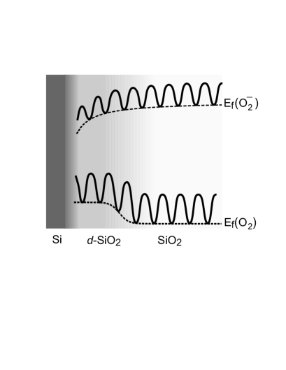
When the diffusing oxygen molecule approaches the Si substrate, two different interfacial effects acting on the neutral and the negatively charged O2 molecule need to be considered. -ray reflectivity measurements indicate the occurrence of a densified interfacial oxide, showing a density of 2.4 g/cm3 and extending over a distance of about 10 Å.Kosowsky_APL_1997 The occurrence of a densified oxide affects the incorporation energy of the neutral O2 molecule which depends on the size of interstitial voids.Bongiorno_PRL_2002 Consequently, the average formation energy of neutral O2 in the densified oxide increases by 0.6 eV.Bongiorno_JPCM_2003 ; Bongiorno_PRL_2002 This picture is confirmed by both selected calculations on our interface model and recent results in the literature.Ohta_PRB_2008 ; Tsetseris_PRL_2006 Figure 2 schematically illustrates this effect showing the evolution of the formation energy of the neutral O2 as it approaches the interface. In the following, we express the correction with respect to the bulk formation energy as , where is the distance to the substrate.
The formation energy of the negatively charged oxygen molecule mainly results from the formation of a bond with a Si atom of the oxide network and is therefore not very sensitive to the modified structural properties of the near-interface oxide. However, as the negatively charged species approaches the silicon substrate, it undergoes stabilization because of the image-charge interaction arising from the dielectric discontinuity at the interface. From classical electrostatics, the stabilization energy reads
| (2) |
where and are the static dielectric constants of Si and SiO2, respectively. This effect is also illustrated in Fig. 2.
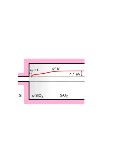
As a consequence of the two effects discussed above, the charge transition level also evolves as the O2 molecule approaches the interface:
| (3) |
where corresponds to the charge transition level in bulk SiO2. We remark that both effects concur to lower . To provide a quantitative estimate, we adopted for the position determined within the mixed scheme, viz. at 1.1 eV above the silicon conduction band minimum. The resulting evolution of is shown in Fig. 3. We found that the charge transition level lies above the Si conduction band edge as long as the distance of the O2 to the Si substrate exceeds 1 Å.note At this small distance the oxidation reaction is already under way,Bongiorno_PRL_2004 suggesting that the negatively charged oxygen molecule plays only a minor role during silicon oxidation. The presence of charged oxygen species had previously been invoked to explain the growth kinetics in the thin-oxide regime.Stoneham_PRB_2001 However, alternative mechanisms based on a spatially varying diffusion rate do not require the charging of the diffusing O2 molecule.Bongiorno_PRL_2004 ; Watanabe_PRL_2006 In the present picture, the neutral O2 interstitial is the dominating oxidizing agent. Other oxygen species can only occur upon the reaction of O2 with Si-Si bonds.Bongiorno_PRL_2004
In conclusion, we addressed the charge state of the O2 molecule during silicon oxidation overcoming the band-gap problem through a scheme based on hybrid density functionals. The oxygen molecule is found to diffuse in its neutral charge state until the onset of oxidation. More generally, the defect level alignment scheme proposed in this work is expected to be very useful for addressing charging issues associated to defects at interfaces.
Support from the Swiss National Science Foundation (Grants Nos. 200020-111747 and 200020-119733) is acknowledged. The calculations were performed on the Blue Gene of EPFL, at DIT-EPFL and CSCS.
References
- (1) S. M. Sze, Physics of Semiconductor Devices (John Wiley & Sons, New York, 1981).
- (2) J. Robertson, Rep. Prog. Phys. 69, 327 (2006).
- (3) P. Broqvist, A. Alkauskas, and A. Pasquarello, Appl. Phys. Lett. 92, 132911 (2008).
- (4) P. E. Blöchl and J. H. Stathis, Phys. Rev. Lett. 83, 372 (1999).
- (5) C. J. Sofield and A. M. Stoneham, Semicond. Sci. Technol. 10, 215 (1995).
- (6) B. E. Deal and A. S. Grove, J. Appl. Phys. 36, 3770 (1965).
- (7) A. Bongiorno and A. Pasquarello, Phys. Rev. Lett. 88, 125901 (2002); Phys. Rev. B 70, 195312 (2004).
- (8) T. Bakos, S. N. Rashkeev, and S. T. Pantelides, Phys. Rev. Lett. 88, 055508 (2002).
- (9) A. Bongiorno and A. Pasquarello, Phys. Rev. Lett. 93, 086102 (2004).
- (10) W. Orellana, A. J. R. da Silva, and A. Fazzio, Phys. Rev. Lett. 87, 155910 (2001).
- (11) K. Kato, T. Uda, and K. Terakura, Phys. Rev. Lett. 80, 2000 (1998).
- (12) H. Watanabe et al., Phys. Rev. Lett. 80, 345 (1998).
- (13) L. Tsetseris and S. T. Pantelides, Phys. Rev. Lett. 97, 116101 (2006).
- (14) H. Kageshima and K. Shiraishi, Phys. Rev. Lett. 81, 5936 (1998).
- (15) A. M. Stoneham, M. A. Szymanski, and A. L. Shluger, Phys. Rev. B 63, 241304 (2001); Solid-State Elec. 45, 1233 (2001).
- (16) A. M. Stoneham, C. R. Grovenor, and A. Cerezo, Phil. Mag. B 55, 201 (1987).
- (17) P. J. Jorgensen, J. Chem. Phys. 37, 874 (1962); D. N. Modlin and W. A. Tiller, J. Electrochem. Soc. 132, 1659 (1985).
- (18) J. Muscat, A. Wander, and N. M. Harrison, Chem. Phys. Lett. 342, 397 (2001).
- (19) J. P. Perdew, K. Burke, and M. Ernzerhof, Phys. Rev. Lett. 77, 3865 (1996).
- (20) J. P. Perdew, M. Ernzerhof, and K. Burke, J. Chem. Phys. 105, 9982 (1996).
- (21) F. Gygi and A. Baldereschi, Phys. Rev. B 34, 4405 (1986).
- (22) http://www.quantum-espresso.org.
- (23) CPMD, Copyright IBM Corp 1990-2006, Copyright MPI für Festkörperforschung Stuttgart 1997-2001.
- (24) F. Giustino and A. Pasquarello, Phys. Rev. Lett. 95, 187402 (2005).
- (25) A. Bongiorno et al., Phys. Rev. Lett. 90, 186101 (2003); A. Bongiorno and A. Pasquarello, Appl. Phys. Lett. 83, 1417 (2003).
- (26) J. Sarnthein, A. Pasquarello, and R. Car, Phys. Rev. B 52, 12690 (1995); Phys. Rev. Lett. 74, 4682 (1995).
- (27) A. Alkauskas et al., Phys. Rev. Lett. 101, 106802 (2008).
- (28) F. J. Himpsel et al., Phys. Rev. B 38, 6084 (1988).
- (29) A. Bongiorno and A. Pasquarello, J. Phys.: Condens. Matter 17, S2051 (2005).
- (30) C. G. Van de Walle and J. Neugebauer, J. Appl. Phys. 95, 3851 (2004).
- (31) G. Makov and M. C. Payne, Phys. Rev. B 51, 4014 (1995).
- (32) During diffusion, the distribution of O2 formation energies has a spread of 0.1 eV due to structural disorder (Ref. Bongiorno_PRL_2002, ). From our calculations, we estimated a spread of 0.4 eV for the O molecule, resulting in a spread of 0.4 eV for . Thermal effects at 1000 K are much smaller.
- (33) P. Broqvist, A. Alkauskas, and A. Pasquarello, Phys. Rev. B 78, 075203 (2008).
- (34) A. Alkauskas, P. Broqvist, and A. Pasquarello, Phys. Rev. Lett. 101, 046405 (2008).
- (35) R. Shaltaf et al., Phys. Rev. Lett. 100, 186401 (2008).
- (36) N. Awaji et al., Jpn. J. Appl. Phys. 35, L67 (1996); S. D. Kosowsky et al., Appl. Phys. Lett. 70, 3119 (1997).
- (37) A. Bongiorno and A. Pasquarello, J. Phys.: Condens. Matter 15, S1553 (2003).
- (38) H. Ohta, T. Watanabe, and I. Ohdomari, Phys. Rev. B 78, in press (2008).
- (39) Furthermore, the derived distance of 1 Å is likely overestimated because of the divergent nature of the image-charge potential in classical electrostatics.
- (40) T. Watanabe, K. Tatsumura, and I. Ohdomari, Phys. Rev. Lett. 96, 196102 (2006).