Scaling of 1/f noise in tunable break-junctions
Abstract
We have studied the voltage noise of gold nano-contacts in electromigrated and mechanically controlled break-junctions having resistance values that can be tuned from (many channels) to k (single atom contact). The noise is caused by resistance fluctuations as evidenced by the dependence of the power spectral density on the applied DC voltage . As a function of the normalized noise shows a pronounced cross-over from for low-ohmic junctions to for high-ohmic ones. The measured powers of and are in agreement with -noise generated in the bulk and reflect the transition from diffusive to ballistic transport.
pacs:
72.70.+m,73.63.Rt,73.40.Cg,85.40.Qx,66.30.QaI Introduction
The study of fluctuations (noise) in physical properties of condensed matter has been an active area of research for decades and has led to profound insights into time-dependent physical phenomena Bak87 ; vdZiel54 ; Kogan96 ; Blanter2000 ; Beenakker2003 . In case of charge transport, the noise shows up as a fluctuating time-dependent AC-voltage over the device with resistance . The most generic noise contributions stem from equilibrium thermal fluctuations of the electron-bath (Johnson-Nyquist noise) Johnson27 ; Nyquist28 , non-equilibrium shot noise caused by the granularity of charge Schottky18 , and resistance fluctuations Hooge69 ; Voss76 ; Bell80 ; Hooge81 ; Dutta_Horn_81 ; Keshner82 ; Giordano83a ; Giordano89 ; Weissmann88 ; Vandamme94 . Whereas thermal and shot noise are frequency independent, resistance fluctuations display a strong dependence which often closely follows a relation over a large frequency range. Because of the dependence, this noise contribution dominates over thermal and shot-noise at lower frequencies. -noise has intensively been studied for bulk and thin film conductors Hooge69 ; Voss76 ; Bell80 ; Hooge81 ; Dutta_Horn_81 ; Keshner82 ; Giordano83a ; Giordano89 ; Weissmann88 ; Vandamme94 , in particular as a diagnostic tool for the technologically relevant electromigration mechanism Sorbello91 ; Vandamme94a ; Dagge96 ; Dong2006 . Noise at low and high frequencies has also been explored in small constrictions Yanson82 ; Yanson84 ; Ralls91 ; Holweg92 , nano-electronic devices Martinis92 ; Birk95 , quantum point-contacts Liefrink92 , sub-micron interconnects Neri97 ; Bid05 , quantum coherent, quasi-ballistic and ballistic nanowires Birge89 ; Strunk98 ; Birge99 ; Neuttiens2000 ; Collins2000 ; Snow2004 ; Fuhrer2006 ; Onac2006 , as well as tunneling contacts Moeller89 ; Jiang90 .
The power-spectral density of resistance fluctuations can phenomenologically be described by Hooge’s law Hooge81 ; Hooge69 :
| (1) |
expressing proportionality of with a frequency dependence. The proportionality factor is ascribed to a material parameter containing the strength of elastic and inelastic scattering, on the one hand, and to an extensive variable , on the other hand. The constant denotes the number of statistically independent fluctuators in the volume. It is straightforward to derive this dependence by assuming a resistance network with resistors in series (or in parallel), all fluctuating independently. The total square fluctuation is then inversely proportional to . In bulk conductors, the total number of electrons has been used for the variable Hooge81 ; Giordano83a ; Hooge90 . Partial support for this view comes from semiconductors in which the carrier density can be changed over many orders of magnitude Hooge90 ; Tacano93 ; Vandamme2000 . Hooge’s law therefore states that -noise is a bulk phenomenon, originating homogeneously over the whole volume. In structures of reduced dimensionality, such as thin films and nanowires, where the surface may dominate over the bulk, the leading contribution to -noise may stem from surface roughness and its fluctuations Sah66 ; Hooge69 ; Vandamme89 ; Wong90 . The validity of bulk scaling of has therefore been questioned. However, there are no quantitative studies on the scaling behavior of -noise in nanocontacts with tunable cross sections in which this dependence could be explored.
In this paper we report on -noise measured in tunable metallic nano-constrictions obtained through electromigration (EM) Park1999 and mechanically controlled break-junctions (MCBJs) Ruitenbeek96 ; Scheer97 ; Agrait2003 . Our emphasis is on the role of the scaling parameter in nano-contacts in the regime of few transport channels where the transition from diffusive to ballistic transport takes place. This transition is observed in our experiments at room temperature and we demonstrate that even in nanocontacts with only a few transport channels, -noise is a bulk property.
II Experimental setup and calibration
Representative examples of EM junctions and MCBJs are shown in Fig. 1a-b. They are both fabricated using electron-beam lithography and metal deposition in a lift-off process. In both cases Au wires with narrow constrictions with typical dimensions of nm in length and nm in width are defined first. Each wire has four terminals enabling the accurate measurement of the electrical resistance. Au wires are fabricated on oxidized ( nm) Si substrates for EM junctions, and on a flexible substrate for MCBJs, onto which a several m thick insulating polyimide layer is cast Grueter2005 . To form an EM junction the four terminals are used in an automatic feedback controlled EM process which continuously shrinks the wire constriction down to an atomic-sized nanojunction as seen in Fig. 1a Wu2007 . In MJBJs the wire constriction is first transferred into a suspended bridge by etching the underlying polyimide layer in an oxygen plasma as seen in Fig. 1b. By bending the substrate the constriction can be narrowed in a controlled manner Ruitenbeek96 ; Scheer97 ; Agrait2003 .
Before narrowing the constrictions, the as-fabricated devices have a junction resistance of around at room temperature as determined in a four terminal setup. The two-terminal resistance , which includes the lead resistance on both sides, amounts to as much as . Because in virgin devices, the feedback-controlled process is mandatory to initiate a nondestructive narrowing by EM Wu2007 ; Trouwborst06 . In voltage-biased controlled EM, in which the voltage over the junction is stabilized by a fast analog feedback Wu2007 , a narrowing sets in at a voltage of V. The junction resistance then rapidly evolves from a few Ohms to . In this regime of active EM, can further be increased into the k-regime by increasing the junction voltage. An example of this process is shown in Fig. 1c. We emphasize that we do not measure the noise while EM proceeds. After narrowing the constriction at a ‘large’ voltage we switch the applied voltage back to values V. During noise measurements, the junctions remain stable. In contrast to EM junctions, MCBJs have the advantage that the junction size can be changed with an independent control parameter by mechanical bending. This allows to change the junction diameter while monitoring noise simultaneously.
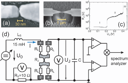
We perform noise measurement in a four terminal setup schematically shown in Fig. 1d. An adjustable low noise DC voltage source is connected via a series inductor and a series resistor to contacts and on the left side, driving a DC bias current through the junction. is used to measure and mH serves to decouple AC from DC. The impedance of the inductor prohibits the shunting of the AC voltage fluctuations (noise). This only works if ( is the angular frequency ), defining a lower cut-off for the useful frequency window. The frequency-dependent noise is simultaneously measured on terminal and and fed into two low-noise preamplifiers (EG&G5184) and a spectrum analyzer (HP89410A). Here, the effective input capacitance is diminishing the signal at high frequencies defining an upper cut-off for the frequency window through the relation . For a typical junction resistance of and effective capacitance nF, the useful frequency window spans approximately three orders of magnitude, i.e. kHz MHz. We describe the -dependence of the circuit analytically (see below) and use this model to fit the total capacitance which contains parts of the Si chip, the connecting wires and the amplifiers. When measuring noise, the two preamplifiers measure the same fluctuating signal in parallel. The spectrum analyzer is operated in the cross-spectrum mode and determines the Fourier transform of the cross-correlation signal from the two amplifiers:
| (2) |
where denotes the time dependent deviations from the average value of the junction voltage measured on amplifier and , and refers to averaging over . This signal is equivalent to the voltage power-noise spectral density. The correlation techniques can eliminate the voltage noises originating from the two amplifiers because the two amplifiers are independent.
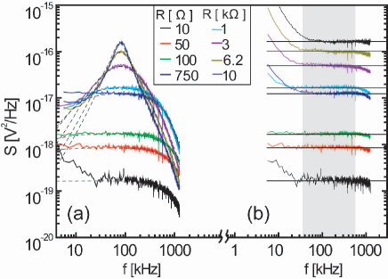
All measurements are done at room temperature ( K) and thermal noise is used to calibrate the setup. The thermal noise of a resistor of value is given by . Due to the -dependent elements in the circuit and the preamplifiers, the noise signal is in general attenuated. The attenuation factor has two components . is determined by the two circuits in Fig. 1d parallel to , the one with the inductor on the left and the one with the capacitor on the right. We obtain for this attenuation factor :
| (3) |
where and where we have assumed that . The second part is due to the frequency-dependent gain of the amplifiers. We have carefully measured this dependence in between Hz and MHz and found that the high-frequency roll-off can accurately be modelled by a first-order low-pass filter with a cross-over frequency of kHz. Hence, is given by:
| (4) |
All parameters , , and the overall gain can accurately be measured except . We therefore determine the capacitance by fitting the frequency dependence of the measured thermal noise to the expected value . A consistent single value of pF has been found for different junction resistances. The validity of this calibration procedure is demonstrated in Fig. 2. In Fig. 2a the frequency dependence of the measured thermal noise is shown for different metal-film calibration resistances ranging between to k which were used instead of a real junction. One can see that the -dependence is very strong for large junction resistance values, whereas a flat -independent part is clearly visible in the opposite case. The expected noise according to is plotted as dashed curves in Fig. 2a. A very good agreement with the measured noise is evident. In Fig. 2b we display the corrected data, i.e. the measured noise divided by the attenuation factor . This procedure works very well in the shaded frequency window over the whole resistance range as evidenced by the flat noise plateaus that coincide with the expected thermal noise (horizontal lines). For the noise study we will therefore restrict the frequency window to the shaded region of kHz.
III Results and Discussion
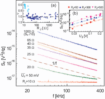
Figure 3 shows the -dependence of for a single EM junction in the ‘low’-ohmic regime with together with a curve representative for large junction resistances (here, k). To measure -noise we typically apply a voltage of mV. This is below the threshold for EM and enables the stable measurements of junctions. Except for the lowest two curves, the main panel of Fig. 3 shows that decays in a power-law fashion, but this decay is not exactly inversely proportional to . This fact has often been noted before: with ranging between and . The latter is expected for a single two-level fluctuator Holweg92 . In our case, the exponent is close to with an average of , taking all data with . What is remarkable, however, is the sample-to-sample fluctuation in the slope (particularly strongly visible in the curve) which we observe universally in all devices.
In addition to the sample-to-sample fluctuation of the slope around a mean-value of , we also see that the bottom curve for the smallest junction resistance of is flat and displays no -noise. This is also true for all devices: -noise only shows up for a sufficient large junction resistance and DC-bias . This is because the thermal noise of the series connection dominates at a small bias and small . After increasing at constant , the -dependence of sets in. The dependence shows up first on the low frequency side. At the high frequency side the thermal noise still dominates. This leads to the impression that the spectrum is flatter than in this transition regime from ‘low’ to ‘large’ values. The deduced power in the relation is shown in the inset (a) of Fig. 3. The open symbols belong to junctions with too low that do not display -noise in the given frequency interval and for applied voltage. Only the filled symbols correspond to junctions displaying full -noise. There is quite some scatter in , but all values stay close to .
In order to shed light on the origin of the -noise, the voltage dependence of has been analyzed. The second inset (b) of Fig. 3 shows taken at a fixed frequency of kHz as a function of . The different symbols refer to three representative samples with , and . There is a strong increase of with which is in quite good agreement with a quadratic dependence, i.e. , for not too large voltages ( V). This quadratic dependence agrees with our expectation for resistance fluctuations as the source of -noise. This expression can be understood by noting that the fluctuating junction resistance generates the fluctuating voltage over the junction at a constant DC bias current . The mean square fluctuation, i.e. the noise, is then proportional to and therefore also to .
Having established the dependence and confirmed resistance fluctuations as its origin, we consider next the prefactor . of many samples has been measured as a function of the junction cross-section, i.e. as a function of , and the contribution was extracted within the frequency interval kHz following the procedure described before. To compare the magnitude of for different samples and different junctions, we now take the normalized noise at a fixed frequency of kHz.
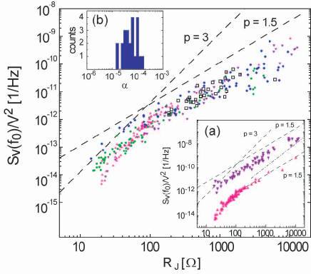
In Fig. 4 (main panel) we show a scatter plot of as a function of of a few samples in a double-logarithmic representation. Four sets were obtained with MCBJ samples and one with a EM one (open squares). Note, that EM samples typically cover only the regime , because when EM sets in, there is a relatively fast transition from the low-ohmic regime I in Fig. 1c to the intermediate resistance regime II. The scatter plot clearly displays a cross-over from a powerlaw dependence with a large power for low and a smaller one for large . This cross-over is better seen in inset (a). Although there are some sample to sample variations, we always observe a cross-over in all of our samples in the vicinity of . The deduced powers are consistent with and for large and low , respectively. The transition and the deduced values are in agreement with -noise generated in the bulk together with a transition from the diffusive to the ballistic transport regime with increasing as we will outline in the following.
It has been pointed out by Hooge Hooge90 , that -noise is a bulk phenomenon, whose scaling parameter (see eq. 1) should grow like the volume . Although this has been disputed and was discussed many times over the last two decades, we will assume scaling with volume and compare to scaling with the surface afterwards. Let us denote a characteristic length of the junction by . In order to refer to size-scaling, we use the terminology length, which reads “length scales with ”. Obviously, . In a diffusive wire of length and cross-section , the resistance is given by , where is the specific resistance. Hence, . Because (eq. 1), we expect in this transport regime. If the characteristic length of the junction becomes shorter than the momentum scattering mean-free path, one is entering the ballistic regime. In this regime, the conductance is determined by the number of transport channels which is proportional to the junction area. The corresponding junction resistance is the so called Sharvin resistance Sharvin65 . Hence, . Consequently, . The data in Fig. 4 shows a crossover which agrees with these derived exponents.
As a comparison, we also derive the expected power, if transport is ballistic and the fluctuators leading to -noise are only present on the surface. All transport channels in the interior of the junction are assumed to be noiseless. Now, will be inversely proportional to , where stands for the number of transport channels on the surface. This number scales as the circumference, and therefore . Using the Sharvin resistance for a ballistic contact we arrive at . Although is not much different than , we are able to distinguish between the two values. In inset (a) of Fig. 4 the dash-dotted line corresponds to . It is clear that the slope of the measured data points is smaller proving that even in small metallic junctions, in which only a few channels carry the charge current, all of them contribute to -noise and not only the channels close to the surface.
Finally, we can estimate the parameter in eq. 1. This parameter corresponds to the noise value for at Hz. If we associate with the number of electrons (which for Au is the same as the number of atoms), we have to look at the value for the single atom contact. Because is then given by the quantum resistance k, we find from Fig. 4 Hz-1. Multiplying with kHz yields . values deduced in this way are shown as a histogram in inset (b) of Fig. 4. This range of -values compares very well with parameters reported in the literature Holweg92 .
IV Conclusions
In conclusion, we have studied -noise at room temperature in tunable electromigration and mechanical controllable break junctions made from Au in a regime in which only a few number of transport channels () contribute to the overall conductance. The transition from the diffusive to the ballistic transport regime is clearly visible in the normalized noise when plotted against the junction resistance . This transition appears at . We find that even in the smallest junctions, -noise is a bulk property.
V Acknowledgement
This work has been supported by the Swiss National Center (NCCR) on Nanoscale Science , the Swiss National Science Foundation, and the University of Basel.
References
- (1) P. Bak, C. Tang, and K. Wiesenfeld Phys. Rev. Lett. 59, 381 (1987).
- (2) A. van der Ziel, Noise, (Prentice-Hall, Englewood Cliffs, 1954).
- (3) Sh. Kogan in ‘Electronic noise and fluctuations in solids’ (Cambridge Univ. Press, 1996).
- (4) Ya. M. Blanter and M. Büttiker, Phys. Rep. 336, 1 (2000).
- (5) C. Beenakker and C. Schönenberger, Phys. Today 56, 37 (2003)
- (6) M. B. Johnson, Phys. Rev. 29, 367 (1927).
- (7) H. Nyquist, Phys. Rev. 32, 110 (1928).
- (8) W. Schottky, Ann. Phys. (Leipzig) 57, 541 (1918).
- (9) F. N. Hooge, Phys. Lett. A 29, 139 (1969).
- (10) R. F. Voss and J. Clarke, Phys. Rev. B 13, 556 (1976).
- (11) D. A. Bell, J. Phys. C (Solid State Physics) 13, 4425 (1980).
- (12) F. N. Hooge, T. G. M. Kleinpenning and L. K. J. Vandamme, Rep. Prog. Phys. 44, 479, (1981).
- (13) P. Dutta and P. M. Horn, Rev. Mod. Phys. 53, 497 (1981).
- (14) M. S. Keshner, Proc. IEEE 70, 212, (1982).
- (15) D. M. Fleetwood, J. T. Masden, and N. Giordano, Phys. Rev. Lett. 50, 450 (1983).
- (16) N. Giordano, Rev. Solid State Science 3, 27 (1989).
- (17) M. B. Weissmann, Rev. Mod. Phys. 60, 537 (1988).
- (18) L. K. J. Vandamme, Xiasong Li, and D. Rigaud, IEEE Trans. Elect. Dev. 41, 1936, (1994).
- (19) R. S. Sorbello, in Material Reliability Issues in Microelectronics Symposium, page 3-13, J. R. Lloyd, F. G. Yost, and P. S. Ho (editors), 1991.
- (20) L. K. J. Vandamme, IEEE Trans. Elect. Dev. 41, 2176, (1994).
- (21) K. Dagge, W. Frank, A. Seeger, and H. Stoll, Appl. Phys. Lett. 68, 1198 (1996).
- (22) J. Dong and B. A. Parviz, Nanotech. 17, 5124 (2006).
- (23) I.K. Yanson, A.I. Akimenko and A.B. Verkin, Solid State Communications, 43, 765, (1982).
- (24) A. I. Akimenko, A. B. Verkin, and I. K. Yanson, J. Low Temp. Phys. 54, 1573 (1984).
- (25) K. S. Ralls and R. A. Buhrman, Phys. Rev. B 44, 5800 (1991).
- (26) P. A. M. Holweg, J. Caro, A. H. Verbruggen, and S. Radelaar, Phys. Rev. B 45, 9311 (1992).
- (27) G. Zimmerli, T. M. Eiles, R. L. Kautz, and J. M. Martinis, Appl. Phys. Lett. 61, 237 (1992).
- (28) H. Birk, M. J. M. de Jong, and C. Schönenberger, Phys. Rev. Lett. 75, 1610 (1995).
- (29) F. Liefrink, A. J. Scholten, C. Dekker, J. I. Dijkhuis, B. W. Alphenaar, H. van Houten, and C. T. Foxon, Phys. Rev. B 46, 15523 (1992).
- (30) B. Neri, C. Ciofi, and V. Dattilo, IEEE Trans. Elect. Dev. 44, 1454 (1997).
- (31) Aveek Bid, Achyut Bora and A. K. Raychaudhuri, Phys. Rev. B, 72, 113415, (2005)
- (32) N. O. Birge, B. Golding, W. H. Haemmerle, Phys. Rev. Lett. 62, 195 (1989).
- (33) C. Strunk, M. Henny, C. Schönenberger, G. Neuttiens, and C. Van Haesendonck, Phys. Rev. Lett. 81, 2982 (1998).
- (34) D. Hoadley, P. McConville, and N. O. Birge, Phys. Rev. B. 60, 5617 (1999).
- (35) G. Neuttiens, C. Strunk, C. Van Haesendonck, and Y. Bruynseraede, Phys. Rev. B 62, 3905 (2000).
- (36) P. G. Collins, M. S. Fuhrer, and A. Zettl, Appl. Phys. Lett. 76, 894 (2000).
- (37) E. S. Snow, J. P. Novak, M. D. Lay, and F. K. Perkins, Appl. Phys. Lett. 85, 4172 (2004).
- (38) M. Ishigami, J. H. Chen, E. D. Williams, D. Tobias, Y. F. Chen, and M. S. Fuhrer, Appl. Phys. Lett. 88, 203116 (2006).
- (39) E. Onac, F. Balestro, B. Trauzettel, C. F. J. Lodewijk, and L. P. Kouwenhoven, Phys. Rev. Lett. 96, 026803 (2006).
- (40) R. Möller, A. Esslinger, and B. Koslowski, Appl. Phys. Lett. 55, 2360 (1989).
- (41) Xiuguang Jiang, M. A. Dubson, and J. C. Garland, Phys. Rev. B 42, 5427 (1990).
- (42) F. N. Hooge, Physics B 162, 344 (1990).
- (43) M. Tacano, IEEE Trans. Electr. Dev. 40, 2060 (1993).
- (44) E. P. Vandamme and L. K. J. Vandamme, IEEE Trans. Electr. Dev. 47, 2146 (2000).
- (45) C. T. Sah and F. Hielscher, Phys. Rev. Lett. 17, 956 (1966).
- (46) L. K. J. Vandamme, IEEE Trans. Electr. Dev. 36, 987 (1989).
- (47) H. Wong, Y C Chng and G Ruan, J. Appl. Phys., 67, 312, (1990)
- (48) H. Park, A. K. L. Lim, J. Park, J., A. P. Alivisatos, and P. L. McEuen, Appl. Phys. Lett. 75, 301 (1999).
- (49) J. M. van Ruitenbeek, A. Alvarez, I. Pineyro, C. Grahmann, P. Joyez, M. H. Devoret, D. Esteve and C. Urbina, Rev. Sci. Instrum. 67, 108, (1996).
- (50) E. Scheer, P. Joyez, D. Esteve, C. Urbina, and M. H. Devoret, Phys. Rev. Lett. 78, 3535 (1997).
- (51) N. Agrait, A. L. Yeyati, and J. M. van Ruitenbeek, Phys. Rep. 377, 81 (2003).
- (52) Zheng Ming Wu, M. Steinacher, R. Huber, M. Calame, S. J. van der Molen, and C. Schönenberger, Appl. Phys. Lett. 91, 053118 (2007).
- (53) L. Grüter, M. T. Gonzalez, R. Huber, M. Calame, and C. Schönenberger, Small 1, 1067 (2005).
- (54) M.L. Trouwborst, S.J. van der Molen, and B.J. van Wees, J. Appl. Phys., 99, 114316, (2006)
- (55) Y. V. Sharvin, Soviet Phys. JETP, 21, 655, (1965)