Directional photoelectric current across the bilayer graphene junction
Abstract
A directional photon-assisted resonant chiral tunneling through a bilayer graphene barrier is considered. An external electromagnetic field applied to the barrier switches the transparency in the longitudinal direction from its steady state value to the ideal at no energy costs. The switch happens because the a.c. field affects the phase correlation between the electrons and holes inside the graphene barrier changing the whole angular dependence of the chiral tunneling (directional photoelectric effect). The suggested phenomena can be implemented in relevant experiments and in various sub-millimeter and far-infrared optical electronic devices.
pacs:
73.23.Hk, 73.63.Kv, 73.40.GkI Introduction
Electromagnetic properties of the bilayer grapheneKats-C ; Novos ; McCann ; Nilsson offer enormous opportunities for scientific research and various nanoelectronic applications. They emerge in spectroscopy of bound and scattering states, in the photon-assisted chiral tunneling and in direct probing of strong correlation effects. Potential applications include electromagnetic field (EF) spectral analyzers, receivers, detectors, and sensorsMy-PRB . The crystal lattice of the bilayer grapheneKats-C ; Novos ; McCann ; Nilsson consists of four equivalent sublattices of carbon atoms while the charge carriers behave there as massive ”chiral fermions”Kats-C ; McCann ; Nilsson . The chiral fermions (CF) in bilayer graphene have a finite mass , like conventional electrons () and holes () in metals and semiconductorsKats-C ; McCann ; Nilsson . The chirality relates the particles to certain sublattice and is responsible for various unconventional d.c. electronic and magnetic properties of the bilayer grapheneKats-C ; Novos ; McCann . In contrast to an ordinary tunneling through a conventional potential barrier, during the chiral tunneling (CT) an incoming electron is converted into a hole moving inside the graphene barrier in a reverse direction as indicated in Fig. 1(a) (Klein paradoxStrange ; Krekora ). This yields a finite transparency for incident electrons with energies below the barrier ( is the barrier height energy) occurringKats-C at finite particle incidence angles . On the other hand, the steady state chiral tunneling is blocked () in the longitudinal direction . The angle-dependent transparency makes the chiral tunneling being attractive for various nanoelectronic applicationsMy-PRB ; Torres . The potential barrier in graphene can either be induced by the gate voltage from a Si gate slab or can be formed by three overlapping graphene sheets as shown in Figs. 1(c,d). According to Ref. Kats-C , the d.c. gate voltage shifts the graphene barrier height, which controls the chiral tunneling. That process implies the wavefunction phases of electrons and holes being interconnected with each other in the graphene. The phase correlations during the chiral tunneling can also be directly tuned by applying of an external a.c. field. Controlling of the electron wavefunction phase by an a.c. field had not been accomplished yet and is the subject of this paper. The electronic properties are described by a spinor wavefunction , which components depend on the angle between the electron momentum and the -axis (see Fig. 1). Similar spinor description had formerly been used for Dirac fermionsStrange and for relativistic quasiparticles in single-layer grapheneKats-C ; Novos2 .
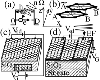
This paper is devoted to electromagnetic properties of a bilayer graphene junction shown in Fig. 1. One may expect that the differential tunneling conductance of ”clean” samples depends on the angle between the electric current and the -direction (see Fig. 1). The whole shape of versus the source-drain voltage is very sensitive to properties of the bilayer graphene barrier. We begin with computing of the steady state curves for a graphene barrier biased by . The steady state results are then utilized for studying of the a.c. properties. When an external electromagnetic field (EF) is applied, it strongly affects the directional diagram of . In particular we will see that the external electromagnetic field induces a finite conductance in the straightforward direction (), which had been blocked in the steady state. That happens because the electromagnetic field affects the electron-hole phase correlations inside the graphene barrier directly. In the steady state, when the a.c. field is off, the electric current is fully suppressed at (for typical gate voltage V and the SiO2 thickness nm one findsNovos2 meV).
II Photon-assisted chiral tunneling
Here we examine influence of an electromagnetic field to chiral tunneling and discuss the intrinsic noise. For studying of the non-stationary electric current across the bilayer graphene junction we implement methodsYeyati ; Keldysh ; Datta . The graphene bilayer is modelled as two coupled gexagonal lattices consisting of four non-equivalent sites A, B and Ã, B̃ in the bottom and top layers respectively [see Fig. 1(a)]. The chiral fermion Hamiltonian operates in space of the two-component wave functions . When the junction is exposed to an external electromagnetic field, the main part of the Hamiltonian is
| (1) |
where , , are the Pauli matrices, , the effective mass is expressed via coupling strength between and as , where , nm is the lattice constant, eV, are corresponding components of the time-dependent vector potential , is the graphene barrier potential controlled by the gate voltage . Eq. (1) describes interlayer coupling via a dimer state formed by pairs of carbon AB̃ atoms located in the bottom and top layers respectively as shown in Fig. 1(b). A weak direct AB̃ coupling and a small interaction due to the bottom and top layer asymmetry (which opens a minigap in the electron spectrumMcCann ) are both hereafter neglected.
For graphene junctions having finite dimensions, the motion of chiral fermions is quantized. The quantization imposes additional constrains on the directional tunneling diagram. Permitted values of the angle inside the graphene barrier are obtained from boundary conditions along the -direction, so the -component of the electron momentum is quantized as (where is the barrier width), which gives where . The last formula also means that depends on the electron energy variable . The electric current density ( is the electric current, is the bias voltage, and is the graphene stripe width) between the electrodes 1 and 3 is computed as where we introduced the factor . If 1 and 3 electrodes are made of a monolayer graphene or are metallic, then where and are corresponding Fermi velocity and the electron density of states at the Fermi level. However if the 1,3 electrodes are made of the bilayer graphene itself, which case we inspect in details below, then where and are the energy dependent velocity and the two-dimensional electron density of states in the bilayer graphene, is the -th electron energy level in the graphene barrier stripe, is the Keldysh Green functionKeldysh , is the electrode index, is the Kronecker symbol, is the distribution function of electrons with momentum . A straightforward calculation using methods of Refs. Yeyati ; Keldysh ; Datta gives
| (2) | |||||
Taking for simplicity from Eq. (2) one finds the zero-temperature steady-state conductance as
| (3) |
where is the graphene barrier transparency. In Eq. (3) we introduced the voltage-dependent dimensionless number of conducting channels . The dependence versus stems from the energy dependence of the electron velocity in the bilayer graphene . Eq. (3) coincides with well known Landauer formula with the number of conducting channels . The calculation results will be convenient to normalize to an auxiliary conductivity defined as (where we used at , being the graphene barrier height). The transmission amplitude across the voltage biased junction is obtained within a simple model which represents the chiral fermion wavefunctions via Airy functions. The Hamiltonian (1) yields a gapless semiconductor with massive chiral electrons and holes having a finite mass . Let us consider tunneling of those fermions with the energy incident on the barrier under the angle . Since the potential barrier is formed in the longitudinal direction, the -component of the momentum is conserved while the -component is not. The trial chiral fermion wavefunction takes a piece-wise formKats-C . The chirality has no significance for particles propagating above the barrier . An analytical steady state solutionKats-C is obtained at for a rectangular barrier expressing the electron and hole wavefunctions via combinations of plane waves. Matching the continuous boundary conditions one findsKats-C ; Novos ; McCann ; Nilsson the tunneling amplitude for a normal electron incidence () as
| (4) |
where the electron wave vector in the electrode is and inside the barrier is , is the phase drop across the graphene barrier, . For a classic rectangular barrier one instead obtains
| (5) |
Although Eqs. (4), (5) are instructive, the experimentally measured characteristics are relevant rather to a finite bias voltage () across the graphene barrier and finite incidence angles . The electric field in the latter case penetrates inside the bilayer graphene barrier and electrodes, forcing the charge carriers to accelerate. Simplest electron and hole wavefunctions in that case are represented via the Airy functionsKorn rather than via plane waves. The CF wavefunction is obtained from the Dirac equation where is the electron energy. For calculations one uses the tilted barrier potential where is the electric field, which penetrates into the graphene barrier. Then components of the fermion momentum are written as and , where is the barrier thickness, is the electron incidence angle in the electrode 1. The corresponding trial wavefunction is
where , is the electron wave vector in the electrode, is the electron wave vector inside the graphene barrier, , , , , , , , , , , , , , . In the above equations we introduced auxiliary matrices and (where means transpose). The chiral tunneling is pronounced at finite incidence angles and at energies below the barrier.
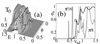
The steady state tunneling probability of a normally incident chiral particle vanishes below the barrier () while is finite above the barrier (when ). In Fig. 2(a) we plot versus the energy of an electron incident to the barrier under the angle . In Fig. 2(b) we show the steady state tunneling differential conductance for different incidence angles . Both the plots in Figs. 2(a,b) are related to meV, which corresponds to the surface charge density cm-2 induced by the gate voltage V across the SiO2 substrate with thickness nm [see Figs. 1(c,d)].
III Directional photo-electric current
The steady state characteristics of the d.c. biased graphene junction described above allow studying of the the external a.c. field influence to the graphene junction. We find that a most spectacular phenomenon occurs when the a.c. gate voltage modulates the height of graphene barrier where is the a.c. field frequency. Then the -component of the electron momentum inside the barrier becomes time-dependent which at gives . We emphasize that a mere factorizationMy-PRB of the electron wave function like [where is not working here since it does not properly incorporate the non-stationary behavior of . The puzzle comes from a non-analytical dependence of on . Therefore one should obtain a valid from corresponding non-stationary boundary conditions at the electrode/barrier interfaces. This gives a complex non-stationary and non-linear behavior of , from which one computes the observable characteristics of interest. The a.c. field induced time dependence yields two spectacular consequences. First, the a.c. field splits the sharp resonance in the energy-dependent transmission probability at as where is the number of photons absorbed during the chiral tunneling process. And second, the a.c. field strongly affects the angular dependence of the chiral tunneling since it renormalizes the angle between and inside the barrier as
| (7) |
In order to compute the time-dependent electric current one solves the non-stationary boundary conditions. In this way one finds the transmission coefficient . Analytical expressions for are obtained in a simplest case (no graphene barrier when the a.c. field is off). After the a.c. field is on, it induces an oscillating potential barrier via an a.c. gate voltage . Assuming a normal incidence () and setting , where is time-dependent one gets
| (8) |
where , . Eq. (8) corresponds to a setup where the graphene barrier is induced purely by the a.c. gate voltage. In the limit of small external a.c. field () from Eq. (8) one obtains
| (9) |
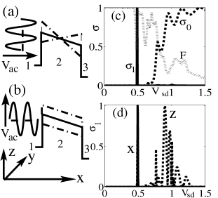
where and we introduced the auxiliary function . The transmission resonances correspond to vanishing denominator , . The Fourier transform of the above equation shows that the a.c. field splits the th chiral tunneling resonance as where is the number of photons absorbed (emitted) during the tunneling. One can see that the external field not only splits the resonances, but also strongly affects angular dependence of the chiral tunneling. That happens because the a.c. field causes no influence to the -component of the electron momentum since the graphene barrier is effectively one-dimensional. The time dependence takes also place when the a.c. field modulates the graphene barrier width as . Splitting of the chiral tunneling resonances, and the angular redistribution of the electric current under the a.c. field influence is better pronounced for a finite barrier height and . From Eq. (7) one can see that if . However if , one may observe a spectacular phenomena. In this case an external a.c. field induces a finite electric current for an almost normal incidence , which was inhibited when the field was off. When , the a.c. field actually causes additional photon-assisted chiral tunneling resonances to engage. The directional photoelectric effect (DPE) may be realized in two scenarios. One scenario assumes that an electron beam having a finite angular width enters the graphene barrier normally. A visible DPE can be achieved in the setup shown in Fig. 4(b) where the attached electrodes 1,3 are made of one-dimensional conducting wires. If the wire is much narrower than the width of graphene stripe (), one may consider the electric current as a result of one-dimensional propagation of of electron along the trajectories under influence of the bias voltage. Such method formerly had intensively been used in numerous works devoted to point contact junctionsKulik ; Yanson . If the electric current is sufficiently weak, the electrons coming from the wire into the graphene stripe introduce a negligible disturbance into the electron spectrum inside graphene. The translational invariance inside graphene is well preservedWildoer . Authors of Ref. Wildoer, used the STM tip for imaging of the electron wavefunction in carbon nanotube which showed a periodic pattern. The electrode 1 emits electrons under a small but finite angle (, ) which trajectories are focused/defocused by the external electromagnetic field as indicated in Fig. 4(b). The frequency dependence of the transparency is governed by the directional photoelectric effect. A significant directional photo-electric effect emerges even for a relatively long wavelength mm - m (which corresponds to the THz domain) if the condition is met. The deviation angle inside the graphene barrier considerably increases giving . This means that an ideal transparency taking place in the steady state at is redistributed over the angle after the a.c. field is applied. The transparency peaks are actually shifted from finite angles to the normal incidence angle . Another scenario involves an incident single electron which enters the graphene barrier strictly normally () under influence of a high frequency THz wave. In this scenario an electron absorbs a THz photon having the finite energy and momentum along the y-axis. Then the electron deviation angle just before entering the barrier is small, . For instance taking THz (which corresponds to the photon energy ) one gets . The photoelectric effect is well pronounced for an electron with energy after it gets inside the graphene barrier. There if the deviation angle increases considerably, since the photon energy is pretty high, , eV. Practically this means that one must set to get a strong photoelectric effect. In the above example the last condition also supposes that one should use meV. Below we consider two most important field polarizations along the and axes as shown in Figs. 3(a,b). The barrier transparency is affected by the a.c. field directly in either case. In particular, the barrier shape is modulated by the a.c. field polarized along the -direction as sketched in Fig. 3(a), since . On other side, if one applies an a.c. field polarized as , it modulates the barrier height since [ is the steady state gate voltage, is the a.c. field induced addition, see sketch in Fig. 3(b)]. Then the a.c. field induced correction to the d.c. tunneling current is , where the transmission amplitude is obtained from corresponding non-stationary boundary conditions at and . Physically, the directional photoelectric effect (DPE) comes from an ingenuous influence of the external electromagnetic field to the electron-hole phase correlations during the chiral tunneling. Technically, modulation of the barrier height by the a.c. field shifts positions of the sharp peaks in the energy-dependent barrier transparency . Besides, it also modifies the overall angular distribution of the electric current, so the electron-hole conversions occur with an additional phase shift. Numerical results for both the cases are presented in Fig. 3(c,d). Corresponding plots for the steady state differential conductance and for the photon-assisted chiral tunneling conductance both indicate the angular redistribution of the photon-assisted chiral tunneling current across the graphene barrier. The steady state conductance curve in Fig. 3(c) corresponds to meV while curve is computed for V and THz. The DPE is well illustrated by the sharp scattering resonance taking place in [see the crisp peak at the incidence angle and at the bias voltage in Fig. 3(c)]. When the a.c. field is off, the steady state tunneling at in the straightforward direction is suppressed [see the corresponding curve for ]. However, if one applies the a.c. field with frequency and , it opens tunneling channels in the straightforward direction as is evident from curve in Figs. 3(c). In Fig. 3(d) we compare two time-averaged conductance curves under influence of the a.c. field with two different polarizations along the (curve X) and (curve Z) axes correspondingly. In either case the curves show remarkable sharp peaks, which position however changes versus the field polarization.
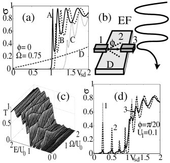
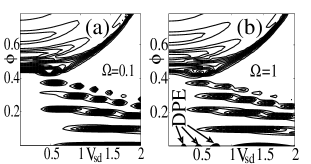
Although the above results are illustrative, they focus solely on the limit of a weak electromagnetic field . Influence of an external electromagnetic field of arbitrary amplitude on the a.c. transport properties of a bilayer graphene junction had been studied in this work using a numeric approach. We solved the non-stationary boundary conditions using the trial function (II) where we take with an arbitrary ratio . We emphasize again that a mere multiphoton approximation like used in Ref. My-PRB, is not working in this case. The graphene barrier transparency now is not assumed to be small, therefore the electron wavefunction cannot be simply factorized as . Therefore we use a straightforward numeric solution of the non-stationary boundary conditions for and compute the time-dependent transmission probability directly from that solution. Then we apply a fast Fourier transform algorithm for computing of numerically versus the external field frequency and the a.c. barrier amplitude . The obtained results for the differential conductance under influence of a strong electromagnetic field with are presented in Fig. 4. In Fig. 4(a) we show the time-averaged conductance of the bilayer graphene junction for the normal electron incidence and for different a.c. field amplitudes (curve A), (curve B), (curve C), and (curve D). One can see that if the external field amplitude is lower than the graphene barrier height (which corresponds to curves A-C) the junction′s conductance has a threshold character versus the bias voltage . If, however, , a finite transparency takes place even at , which corresponds to curve D. From the three-dimensional plot shown in Fig. 4(c) one can see that a visible transparency is achieved at frequencies , which is well consistent with the semi-qualitative consideration above. A more accurate estimation of the DPE magnitude follows from Fig. 4(d) where we plot for three different frequencies (curve 1), (curve 2), and (curve 3). The peaks of finite in curves 1-3 at are present because the electron incidence angle is finite though small (). The peak increase of the junction′s conductance is achieved at selected bias voltage values and , which corresponds to curve 1. One can see that the directional photo-electric effect increases the junction conductance at by a few orders of magnitude as compared to its steady state value at the same . Relevant increase of the conductance is however less significant at other a.c. field frequencies, i.e., (curve 2), and (curve 3). In Figs. 5(a,b) we show contour plots of the time-averaged conductance of a bilayer graphene junction versus the electron incidence angle and the source-drain bias voltage for two different a.c. field frequencies (a) and (b) . The conductance diagrams in either case have pretty spectacular complex structure where the dark spots correspond to . When the external field frequency is low [i.e., as shown in Fig. 5(a)], the tunneling for the incident electron energies is fully blocked. However, when the field frequency becomes higher, i.e., as indicated in Fig. 5(b), one may notice a series of sharp dark spots at discrete energies below the barrier () pronounced at the normal incidence angle . Those dark spots constitute the directional photoelectric effect discussed above and indicated as DPE in Fig. 5(b).
Intrinsic noise in the bilayer graphene junction originates as follows. The thermal noise comes from the phonons emitted in the electron-phonon collisions. Matrix element of the electron-phonon collisions according to Ref. Ando ; McEuen is where is the angle between initial and final states. The phase factor plays quite a different role in the bilayer graphene compared to the single layer grapheneAndo where it is rather instead. In the latter case, the factor ensures suppression of the electron-phonon and electron-impurity collisions and the transport of the change carriers remains ballistic up to room temperatures. In contrast, thermal noise in the bilayer graphene devices is rather high at room temperatures. Another intrinsic noise (Poisson noise) arises due to the ”Zitterbewegung” effect, which is linked to a jittering motion of the change carriers when electrons are randomly converted to holes forth and back. That produces noise even in zero temperature limit. The noise is characterized by the Fano factor , where is the tunneling probability in the -th channel and the summation is performed over all the conducting channels (in our setup this means just integration over ). From the plot shown in Fig. 3(d) for (in units of ) one infers that the Poisson noise becomes extremally low at .
IV Conclusions
In conclusion we computed the electric current across the bilayer graphene junction in conditions when an external electromagnetic field is applied. We have found that the threshold absorption of the external electromagnetic field strongly depends on the a.c. field frequency and amplitude. The electromagnetic field induces an ideal transparency of the graphene barrier in the longitudinal direction, which had been fully suppressed when the a.c. field was off. That directional photoelectric effect originates from an angular redistribution of the whole transparency diagram since the sidebands at finite angles are redirected to the normal incidence. An experimental observation of such a spectacular directional optoelectric phenomena would provide a strong evidence for existence of the massive chiral fermions in the bilayer graphene. We emphasize that the threshold absorption emerges purely from a quantum mechanical phase shift, and not from an inelastic excitation by the a.c. field. That means no heating is involved during the absorption. The a.c. current induced by the electromagnetic field across the graphene junction has a sharp angular dependence, which potentially can be exploited in sensor nanodevices of the external electromagnetic field. The directional photoelectric effect in the double layer graphene junctions is a unique phenomenon which exists in that system and had not been noticed in other systems, like junctions composed of single layer graphene or of normal metals. Most intriguing feature is the switch between zero and finite conductance occurring without energy absorption. The phenomena considered above have a great potential for various nanoelectronic applications.
I wish to thank V. Chandrasekhar and P. Barbara for fruitful discussions. This work had been supported by the AFOSR grant FA9550-06-1-0366.
References
- (1) M. I. Katsnelson, K. S. Novoselov, and A. K. Geim, Nature Phys. 2, 620 (2006).
- (2) K. S. Novoselov, E. McCann, S. Morozov, V. I. Falko, M. I. Katsnelson, U. Zeitler, D. Jiang, F. Schedin, and A. K. Geim, Nature Phys. 2, 177 (2006).
- (3) E. McCann and V. I. Falko, Phys. Rev. Lett. 96, 086805 (2006).
- (4) J. Nilsson, A. H. Castro Neto, F. Guinea, N. M. R. Peres, PRB 76, 165416 (2007).
- (5) S. E. Shafranjuk, Phys. Rev. B76, 085317 (2007).
- (6) L. E. F. Foa Torres, Phys. Rev. B 72, 245339 (2005); L. E. F. Foa Torres and G. Cuniberti, arXiv:0807.4953v2 (unpublished).
- (7) P. Strange, Relativistic Quantum Mechanics (Cambridge University Press, Cambridge, UK, 1998).
- (8) P. Krekora, Q. Su and R. Grobe, Phys. Rev. Lett. 92, 040406 (2004).
- (9) K. S. Novoselov, A. K. Geim, S. V. Morozov, D. Jiang, Y. Zhang, S. V. Dubonos, I. V. Grigorieva, A. A. Firsov, Science 306, 666 (2004);
- (10) A. L. Yeyati and M. Büttiker, Phys. Rev. B 52, R14360 (1995).
- (11) L. V. Keldysh, Sov. Phys. JETP 20, 1018 (1965).
- (12) S. Datta, Electronic Transport in Mesoscopic Systems (Cambridge University Press, Cambridge, UK, 1997).
- (13) G. A. Korn and T. M. Korn, Handbook for Scientists and Engineers, McGraw-Hill (1967).
- (14) I. K. Yanson, Zh. Eksp. Teor. Fiz. 66, 1035 (1974) [Sov. Phys. JETP 39, 506 (1974)].
- (15) R. I. Shekhter and I. O. Kulik, Fiz. Nizk. Temp. 9, 46 (1983) [Sov. J. Low Temp. Phys. 9, 22 (1983)].
- (16) L. C. Venema, J. W. G. Wildöer, J. W. Janssen, S. J. Tans, H. L. J. Temminck Tuinstra, L. P. Kouwenhoven, and C. Dekker, Science 283, 52 (1999).
- (17) T. Ando, T. Nakanishi, and R. Saito, J. Phys. Soc. Jpn., 67, 2857 (1998); T. Ando, T. Nakanishi, J. Phys. Soc. Jpn., 67, 1704 (1998).
- (18) P. L. McEuen, M. Bockrath, D. H. Cobden, Y. G. Yoon, and S. Louie, Phys. Rev. Lett., 83, 5098 (1999).