CdSe quantum dots in ZnSe nanowires as
efficient source for single photons up to 220 K
Abstract
ZnSe nanowire heterostructures were grown by molecular beam epitaxy in the vapour-liquid-solid growth mode assisted by gold catalysts. Size, shape and crystal structure are found to strongly depend on the growth conditions. Both, zinc-blende and wurtzite crystal structures are observed using transmission electron microscopy. At low growth temperature, cone-shaped nano-needles are formed. For higher growth temperature, the nanowires are uniform and have a high aspect ratio with sizes of 1–2 m in length and 20–50 nm in width as observed by scanning electron microscopy. Growing a nanowire on top of a nano-needle allows us to obtain very narrow nanorods with a diameter less than 10 nm and a low density of stacking fault defects. These results allow us the insertion of CdSe quantum dots in a ZnSe nanowire. An efficient photon anti-bunching was observed up to 220 K, demonstrating a high-temperature single-photon source.
An appealing application for semiconductor nanowires (NWs) is the inclusion of quantum dots (QDs) into the NW. Due to the narrow lateral size, NW QD heterostructures can be directly grown on defined positions and without the necessity of self-assembly. This is especially important for for II-VI materials, where self-assembled QD formation occurs only within narrow windows of growth conditions RobinAPL . Recently, II-VI compound semiconductor NWs have been synthesized by Au-catalysed metal-organic chemical vapour deposition (MOCVD) and molecular-beam epitaxy (MBE) methods NW-MOCVD ; NW-MBE ; Colli . QD devices can be utilized as emitters for the effective and controlled generation of single-photon states. Single-photon emission from a GaAsP/GaP NW QD was reported before at cryogenic temperature in ref. Zwiller_NW_AB . High-temperature experiments from individual Stransky-Krastanov (SK) grown QDs were reported from CdSe/ZnSe QDs Sebald and from GaN/AlN QDs Kako . Both experiments showed photon anti-bunching up to 200 K with normalized dip values of 81% and 53%, respectively. Other systems have demonstrated room temperature single photon emission: nanocrystals MichlerNC have the drawback that they suffer from blinking effect BrokmannBlinking ; colour centres in diamond Grangier ; Kurtsiefer have shown very reliable operation but with a very broad spectrum. Anyways, neither nanocrystals nor colour centres in diamond offer the possibility of electrical excitation, which is a very realistic and very promising perspective for semiconducting nanowires MinotNWLED .
In this paper, we report MBE growth of ZnSe NWs on Si and GaAs substrates and insertion of CdSe QDs in these NWs. The growth process is based on the Au-catalyzed VLS method. The morphology of the NWs depending on the growth parameters was examined by scanning electron microscopy (SEM) and high-resolution transmission electron microscopy (HRTEM). We found two different growth regimes, resulting in either narrow and uniform NWs, or cone-shape nano-needles. When combining these growth regimes, NWs with a very low density of defects can be achieved. As an important application of these NW QD structures, we present the generation of single photons from a single QD with a deep anti-bunching of the photon correlation even up to high a temperature of 220 K.

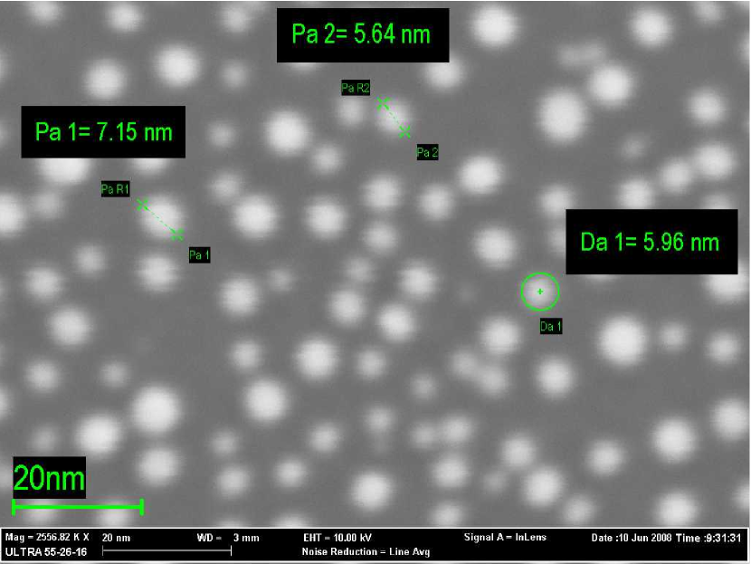
Prior to the growth, the substrates, (100)-, (111)-GaAs and (100)-Si, were annealed in an ultra-high vacuum (UHV) chamber to 580∘ C in order to degas the surfaces. Additionally, the GaAs surface deoxidizes at this temperature, while the Si substrate remains oxidized. A thin Au layer (0.2–1 nm thick) was then deposited on the substrate at room temperature by e-beam metal deposition. The samples were then introduced in a II-VI MBE chamber. The transfer between the MBE and metal deposition chamber were performed under UHV. In order to generate Au nanoparticles, the gold film was dewetted by annealing the substrate to 450∘ C for 10 min. At this temperature, the gold forms nanoparticles, as observed by SEM and AFM (Figure 1(a)). Next, growth of ZnSe wires at different sample temperatures was performed. All samples were grown by solid-source MBE. The growth parameters like growth temperature, Zn:Se flux ratio or gold thickness were varied independently. The growth rate is in the 0.5 nm/s range.

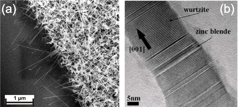
First we studied the effect of the sample temperature on the NW structure, while the beam pressure where kept constant (Zn (Se) flux: 2.5 (7.5) torr). When growing at a substrate temperature within 350-450∘ C, a dense carpet of uniform NWs covers the substrate (fig. 2(a). They have a diameter of about 20–50 nm and a length of 1–2 m. The structure is predominantly a wurtzite structure with [0001]-axis as growth direction. As seen in the TEM image in fig 2(b), stacking faults due to zinc blende insertions are repeatedly observed along the NW. Additionally to the NWs, the substrate is covered with highly irregular nano-structures. The formation of stacking faults and irregular nano-structures are explained by non-ideal growth conditions at the initial stages of the growth process. Possible reasons are the presence of non-uniform gold agglomerations instead of small gold beads and the insertion of impurities during the gold deposition process. The presence of both wurtzite and Zn-blende shows, that at the utilized growth conditions both phases are allowed.

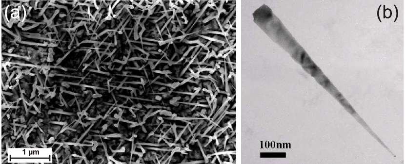
When growing at low temperature (300∘ C), HRTEM and SEM images reveal the formation of nano-needles with a wide base (80 nm diameter) and a sharp tip (5–10 nm diameter) covered by a gold particle as seen in fig. 3. Similar results are obtained at a growth temperature of 450∘ C but with inverted Zn:Se flux ratio. The structure is mainly a wurtzite type with [11-20]-axis as growth direction. Towards the base, the structures are again repeatedly intersected by zinc blende domains, while the tip has a pure wurtzite structure. The formation of nano-needles instead of NWs is well accounted for by the slower adatom mobility expected at low temperature, which promotes nucleation on the sidewalls before reaching the gold catalyst at the nano-needle tip. A similar idea was proposed in ref. Colli for the formation of nanosaws. In contrast to the NWs, the defect planes are here disoriented with respect to the nano-needle axis. It seems that this disorientation hinders the propagation of defects in the growth direction, especially for lower diameters. Defects zones are rapidly blocked on the side walls, providing a higher structural quality towards the nano-needle tip. Interestingly the nanowire structure and shape do depend only little on the underlying substrate.

The observation of a decreasing defect density from the base towards the top in the nano-needles motivated us to modify the growth recipe in the following way: In the first part, the sample is grown with excess of Zn for 30 min, leading to the formation of nano-needles. Next, the Zn- and Se-flux was inverted and NWs were grown for another 30 min on top of the nano-needles. Thus, the growth at the side-walls was aborted and re-growth started on defect-free and strain-relaxed nano-needle tips, where the high structural quality of the crystal lattice can be preserved along the narrow NW that is now formed in this second growth step. Fig. 4 shows results obtained from this sample. The structures have a broad base that tapers after a few ten nanometers to thin NWs with thickness of 10–15 nm. When studying single NWs by HRTEM, we see that the stacking faults indeed strongly reduce towards the thin part of the NW.

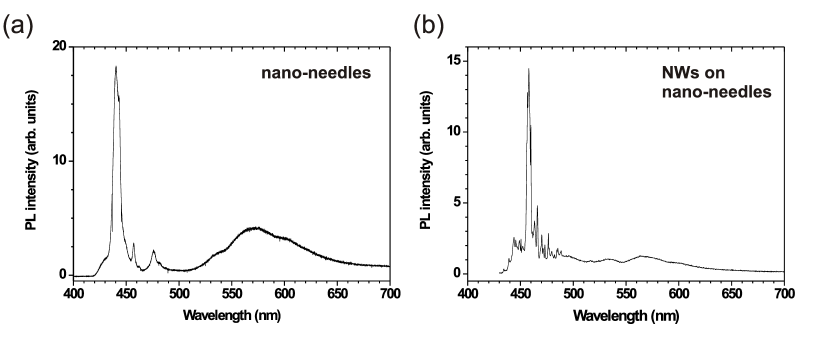
The suppression of such stacking faults becomes important, when observing the spectral properties of a single NW QD. The spectra were taken at a sample temperature of 5 K. The samples were excited by a cw laser at 405 nm via a microscope objective. Fig. 5(a) shows the spectra from an ensemble of nano-needles. The peak at 440 nm belongs to ZnSe bandedge emission. This is mostly due to bulk ZnSe that is grown in parallel to the nano-needles at the sample floor. Single nano-needles and NWs (not shown here) only show a very weak contribution of the ZnSe bandedge. More strikingly, we observed a broad emission within 500–600 nm. This can be attributed to excitons localized at the defect zones in the nano-needle Philipose2 . In contrast, for the combined NW/nano-needle structure, fig. 5(b), this emission is mostly suppressed leaving behind a only a small bunch of spectral lines between 450–500 nm. These are presumably from the broader base of these structures. When isolating single structures (see below), it will most likely break at the narrow NW part, which contains much less defects, so that we find single NWs, in which this broad emission is completely suppressed.
With these conditions, it finally becomes possible to grow and study single NW samples with an inserted CdSe QD. In order to prepare QDs, a small region of CdSe has been inserted in this high quality part of the ZnSe NW. This is done by interrupting the ZnSe growth after 30 min and changing to CdSe for 30 s. Next, the ZnSe growth is continued for another 15 min. The diameter size is of the order of the bulk exciton Bohr diameter for CdSe (11 nm). This means that the carriers in the CdSe QD are in the strong confinement regime. For the study of single NWs, the sample is put in a methanol ultra-sonic bath for 30 s, in which some NW broke off the substrate into the solution. This process allows also to detach mainly the high quality part of the NW from the nano-needles where many stacking faults are present. Droplets of this solution were next placed on a new substrate, leaving behind a low density of individual NWs. Metal markers have been made on the substrate using optical lithography technique in order to locate the NWs.

Fig. 6(b) shows the spectra from a NW QD at different temperatures. The spectral line can be attributed to a trion transition. With higher excitation intensity, also an exciton and biexciton transition become visible. Above 150 K, the spectral lines significantly broaden. We found that the light emission is highly polarized with a contrast of 80–90% (while exciting the NW with circularly polarized laser light). This striking polarization anisotropy of absorption can be explained by the dielectric contrast between the NW material and the surrounding environment, and the orientation of the dipole within the QD LieberPolNW ; NiquetPolNW .
We have carried out photon correlation measurements using a Hanbury Brown and Twiss setup. The sample (few NWs on a silicon substrate with micro-markers) was mounted in a He-flow cryostat. The QD’s were optically excited with a frequency doubled Ti:sapphire laser emitting 200-fs pulses with a repetition rate of 80 MHz. The laser was focused on the sample by using a microscope objective and the luminescence was collected with the same objective. The QD emission passed through a spectrometer and is then sent to a Hanbury Brown-Twiss correlator based on two silicon avalanche photodiodes (APDs) and a coincidence counter.
The graphs in fig. 6(a) are the raw histograms of measured coincidences without any correction for background count events. The area under each peak at time , was normalized with respect to the average area under the peaks at . Each peak area was calculated by integrating the coincidences within 12-ns windows (repetition time of the excitation laser). The correlation functions were taken at different temperatures between 4 K and 220 K. At 4 K, the peak at is suppressed to a normalized value of 7%, showing the high quality of the single-photon generation. With increasing temperature, this value only slightly increases to finally reach 36% at 220 K. This value is far below 50%, the emitted light field is thus clearly distinguished from states with 2 or more photons. Thus, even without correcting for background events, these emitters can be directly used as a high-quality single-photon device even when operating at high temperature, with a strongly suppressed probability for two-photon events. In the correlation measurement obtained at 220 K, a low resolution grating was used in the spectrometer so that all the photons coming from the broader line could be counted. This broader spectral window of integration leads to larger background, which is the main origin for the rise of the -peak above 150 K. In contrast to SK QDs which often grow with a high density on the substrate, the density of NWs in the microscope focus was much smaller and can be even reduced to only one within the microscope focus, which avoids contributions from neighbouring emitters that spectrally overlap with the transition under observation.
In summary, we have performed optical studies on single CdSe QDs in ZnSe NWs. The NWs were developed by MBE in a two-step growth recipe, where narrow, mostly defect-free NWs are grown on top of broader, cone-shaped NWs. The single-NW PL features narrow, isolated spectral lines. When filtering individual transitions, non-classical single-photon statistics were retrieved, indicated by strong anti-bunching, where the raw correlation function was reduced down to a normalized value of 7%. This behaviour remains even up to a temperature of 220 K, where this correlation peak is only slightly increased to 36%. For non-blinking QDs, this is the highest reported temperature for single-photon emission and for an anti-bunching-dip below 50%. At this temperature, Peltier cooling becomes an alternative to liquid helium or nitrogen cooling. Together with the possibility of integrating NWs into electro-optical circuits MinotNWLED , these emitters become an interesting candidate for developing compact, stable and cost-efficient quantum devices operating near room temperature.
Acknowledgements
T.A. acknowledges support by Deutscher Akademischer Austauschdienst (DAAD). Part of this work was supported by European project QAP (Contract No. 15848).
References
- (1) I.-C. Robin, R. André, C. Bougerol, T. Aichele, and S. Tatarenko, Appl. Phys. Lett. 88 (2006), 233103.
- (2) R. Solanki, J. Huo, J. L. Freeouf, and B. Miner, Appl. Phys. Lett. 81 (2002), 3864.
- (3) Y. F. Chan, X. F. Duan, S. K. Chan, I. K. Sou, X. X. Zhang, and N. Wang, Appl. Phys. Lett. 83 (2003), 2665;
- (4) A. Colli, S. Hofmann, A. C. Ferrari, C. Ducati, F. Martelli, S. Rubini, S. Cabrini, A. Franciosi, and J. Robertson, Appl. Phys. Lett. 86 (2005), 153103. .
- (5) M. T. Borgström, V. Zwiller, E. Müller, A. Imamoglu, Nano Lett. 5 5 (2005), 1439.
- (6) K. Sebald, P. Michler, T. Passow, D. Hommel, G. Bacher, and A. Forchel, Appl. Phys. Lett. 81 (2002), 2920.
- (7) S. Kako, C. Santori, K. Hoshino, S. Götzinger, Y. Yamamoto, and Y. Arakawa, Nature Mat. 5 (2006), 887.
- (8) P. Michler, A. Imamoglu, M. D. Mason, P. J. Carson, G. F. Strouse, and S. K. Buratto, Nature 406 (2000), 968.
- (9) X. Brokmann, J.-P. Hermier, G. Messin, P. Desbiolles, J.-P. Bouchaud, and M. Dahan, Phys. Rev. Lett. 90 (2003), 120601.
- (10) R. Brouri, A. Beveratos, J.-P. Poizat, and P. Grangier, Opt. Lett. 25 (2000) 1294.
- (11) C. Kurtsiefer, S. Mayer, P. Zarda, and H. Weinfurter, Phys. Rev. Lett. 85(2000), 290.
- (12) E. D. Minot, F. Kelkensberg, M. van Kouwen, J. A. van Dam, L. P. Kouwenhoven, V. Zwiller, M. T. Borgström, O. Wunnicke, M. A. Verheijen, and E. P. A. M. Bakkers, Nano Lett. 7 (2007), 367.
- (13) U. Philipose, S. Yang, T. Xu, and H. E. Ruda, Appl. Phys. Lett. 90 (2007), 063103.
- (14) J. Wang, M. S. Gudiksen, X. Duan, Y. Cui, and C. M. Lieber, Science 293 (2001), 1455.
- (15) Y. M. Niquet and D. C. Mojica, Phys. Rev. B 77 (2008), 115316.