Interlayer coupling in EuS/SrS, EuS/PbSe and EuS/PbTe magnetic semiconductor superlatices
Abstract
Neutron reflectivity studies of EuS/SrS, EuS/PbSe, and EuS/PbTe all-semiconductor superlattices were carried out in search for exchange interlayer coupling. A relatively weak antiferromagnetic coupling was found in EuS/SrS and in EuS/PbSe systems but no interlayer coupling was detected in EuS/PbTe superlattices. In EuS/SrS, where the SrS spacer is an insulator ( eV), a very weak and short range interlayer coupling is in agreement with the earlier theoretical predictions that the interlayer coupling strength in EuS-based magnetic semiconductor superlattices depends strongly on the energy gap of the nonmagnetic layer and should decrease with an increase of the energy gap of the spacer material. A weak coupling in EuS/PbSe and no coupling in EuS/PbTe, where both PbSe and PbTe are narrow-gap semiconductors ( eV), is in disagreement not only with the theoretical expectations but also in a stark contrast with earlier results for another narrow-gap spacer system – EuS/PbS, where pronounced antiferromagnetic coupling persists even in samples with PbS layer thickness as large as 200 Å. A possible influence of the increasing lattice mismatch between EuS and the spacer materials (0.5%, 0.8%, 2.5%, and 8.2% for PbS, SrS, PbSe, and PbTe, respectively) on the magnetic in-plane ordering of EuS layer and, consequently, on the interlayer coupling was investigated by polarized neutron reflectometry in the case of EuS/PbTe.
pacs:
61.05.fj, 75.50.Pp, 75.25.+z, 75.70.-i1 Introduction
EuS is a well-known ferromagnetic semiconductor. It has been extensively studied since the 1960s, so that its magnetic and electronic properties have been well characterized [1].
Because of its low Curie temperature, EuS ( K) is certainly not a good candidate for practical spintronics applications. However, since its magnetic and electronic properties are well understood, it may serve as a good “prototype” for investigating the fundamental physical mechanisms underlying phenomena that are highly interesting in the context of spintronics studies. Interlayer magnetic coupling in all-semiconductor superlattices is one such topic.
This work is a continuation of earlier studies of interlayer magnetic coupling in EuS/PbS and EuS/YbSe semiconductor superlattices [2, 3] in which a pronounced antiferromagnetic (AFM) interlayer coupling (IC) has been found. All the present and the previous neutron reflectometry experiments were carried out at the NIST Center for Neutron Research, Gaithersburg, USA on the NG-1 neutron reflectometer.
2 EuS/SrS superlattices
The origin of IEC phenomena in all-metallic multilayers is now quite well understood. As shown by a number of theoretical studies backed by experimental results (see, e.g., [4]), the interaction between two metallic FM blocks across a nonmagnetic metallic spacer is maintained by conduction electrons. However, this mode of interaction cannot give rise to any observable interlayer coupling effects in superlattices composed of semiconduting materials in which the concentration of mobile carriers is orders of magnitude lower than in metals.
In order to explain the origin of the pronounced interlayer coupling seen in all-semiconductor SL systems such as EuS/PbS, EuS/YBSe, and EuTe/PbTe, Blinowski and Kacman (B&K) proposed a model in which the exchange interactions are conveyed across the semiconductor spacers by valence band electrons [5]. The model does not assume any particular interaction mechanism, but attributes the interlayer coupling to the sensitivity of the superlattice electronic energies to the magnetic order in the layers – i.e., it accounts globally for the spin-dependent band structure effects. According to the Blinowski and Kacman model, the strength of the coupling between the EuS layers decreases exponentially with the spacer layer thickness. The model also predicts that that exponential decrease is faster for the systems where the energy gap of the spacer material is larger [6]. In other words, weaker and shorter range interactions should be seen in EuS/YbSe ( eV for YbSe) multilayers than in EuS/PbS ( eV for PbS) superlattices. This has been demonstrated experimentally by neutron reflectometry experiments performed in applied magnetic fields [3].
In order to further test the predictions of the B&K theory, we have carried out neutron reflectometry studies of EuS/SrS superlattices.

All three spacer materials, PbSe, YbSe and SrS, have the same structure (NaCl type) as EuS, and are nearly perfectly lattice-matched with EuS. The strain effects in the EuS/SrS system thus remain essentially the same as in EuS/PbS and EuS/YbSe superlattices. PbS is a narrow-gap semiconductor, YbSe is a wide-gap semiconductor, and SrS ( eV) is usually cosidered to be an insulator. Therefore, any changes in the strength and the range of IC in these three systems can be attributed, with a high degree of certainty, only to the differences in electronic band structure of the spacer material.
The results of neutron reflectivity measurements performed on four EuS/SrS superlattices with different structural parameters are presented in the Figure 1. The dot-dashed lines represent the reflectivity profile measured at 30 K, which assures that EuS is still in its paramagnetic phase. The solid lines show the reflectivity measured at 4.6 K (well below the Curie temperature of K) and in zero external magnetic field. In the case of the thinnest (7.5 Å) SrS spacer, two half-order ( and ) superlattice reflections prove the antiparallel alignment of adjacent EuS layer magnetizations. These AFM maxima disappear in sufficiently strong (saturating) applied magnetic field where the magnetization vectors in all EuS layers are aligned parallel to the field. In such a situatuation, the magnetic Bragg maxima occur at the same positions as the structural maxima – in practice it means that the structural Bragg peaks should increase in intensity due to the additional ferromagnetic (FM) contribution. It should be noted, however, that EuS/SrS is a special case of a superlattice system – namely, due to the very small nuclear scattering contrast between EuS and SrS layers (nuclear scattering lengths of Eu and Sr are fm and fm, respectively) the structural SL Bragg peaks are extremely weak and they are not visible against the background in neutron reflectivity spectra (they can be seen only in X-ray reflectivity spectra, and from such measurements one can accurately determine their positions). Magnetic and structural properties of EuS–SrS semiconductor multilayers were studied earlier by SQUID, magneto-optical Kerr effect magnetometry, and by X-ray diffraction methods [7].
On the other hand, due to the very large magnetic moment of the Eu2+ cation (7 ), the magnetic scattering contrast between EuS and nonmagnetic SrS is quite strong. Concsequently, the FM peaks measured at saturating field are clearly visible and well developed, which attests to the good structural quality of the samples.
The AFM SL peak becomes less and less pronounced as the SrS spacer layer grows thicker (to 13 and 27 Å), reflecting the decrease of the AFM interlayer coupling strength with increasing spacer thickness. For the sample with the SrS layer 55 Å thick there is no longer any visible trace of the AFM interlayer ordering.
3 Interlayer coupling in EuS/PbSe and EuS/PbTe superlattices
A similar experimental procedure, to that described above, was applied to the set of EuS/PbSe superlattices. The results obtained from those measurements are summarized in Figure 2.

In contrast to the EuS/SrS data, the spectra from EuS/PbSe specimens exhibit well-developed structural SL Bragg peaks. This comes from the fact that the scattering length values for both constituent elements of the spacer layers are larger than the scattering length values of Eu and S ( fm and and fm, compared to and fm), giving rise to a much larger scattering length density contrast than in the case of EuS/SrS system.
The presence of clearly visible maxima at AFM positions is clear evidence for the existence of significant AFM interlayer coupling in the EuS/PbSe system. The dependence of the AFM peak intensity on the spacer thickness closely resembles the situation seen in the EuS/SrS SL system. However, one would expect much stronger IC effects in EuS/PbSe, considering that the PbSe spacer is a narrow gap semiconductor with an value very close to that in PbS – and in the EuS/PbS system much stronger and longer range IC was in fact observed [3].
As it was decribed earlier [3, 8], in order to evaluate quantitatively the IC strength the AFM peak intensity was measured as a function of applied magnetic field. The results of such experiments performed on EuS/PbS, EuS/PbSe, and EuS/SrS samples are shown in Fig. 3.

The measurement procedure is the following: the sample is first cooled down to the desired temperature in zero magnetic field, and then is kept constant throughout the entire experiment. The intensity of the AFM peak is recorded. Then a magnetic field is applied and increased in constant increments, and the AFM peak intensity is recorded for each value. The procedure is continued until reaches the saturation value (i.e., where the AFM peak completely disappers). The field is then decreased in the same manner back to zero. Next, the field direction is reversed, again increased to the saturation value, and decreased back to zero – then again reversed, and one more up-down cycle is performed. This allows us to measure the ’hysteresis loop’ of the antiferromagnetically coupled superlattice.
All samples we have investigated so far (with the exception of one EuS/PbS (30/4.5) Å specimen which showed essentially no hysteresis effects) remained in the ferromagnetic configuration after the first cycle of the field. Further application of the magnetic field in the opposite direction leads to a partial restoration of the intensity of the AFM peak. From the latter it can be inferred that the antiferromagnetic interlayer configuration can be restored only in a fraction of the sample. How large this fraction is depends on the nonmagnetic spacer type (PbS, YbSe, PbSe or SrS) and its thickness. Thus, for a sufficiently thin PbS spacer (12 Å, see Figure 3(a)) one can observe a full restoration of the initial AFM state (in this particular example the fraction of the AFM coupled sample is even higher than it was in the initial zero-field-cooled state). In the case of PbSe, another narrow-gap semiconductor spacer, the degree of restoration is lower than for a PbS layer of approximately the same thickness (see Fig. 3(b)). This suggests that the AFM coupling strength in the EuS/PbS samples is considerably stronger than in the EuS/PbSe samples with the same spacer thickness. In the case of SrS, which is actually an insulator, the degree of recovery of AFM intensity is far lower than for PbS and lower than for PbSe spacers (see Figure 3(c)) despite the fact that the thickness of SrS layer is considerably smaller, only 7.5 Å. The weakness of IC strength in EuS/SrS is most dramatically visualized in Figure 3(d) for EuS/SrS sample with an 11 Å spacer, where there is no recovery of the AFM peak.
Thus, in summary, for superlattices with PbS, YbSe and SrS spacers, which are all very well lattice-matched with EuS, interlayer interactions systematically decrease as the energy-gap of the spacer material increases. This finding fully corroborates the theoretical predictions of Blinowski-Kacman tight-binding calculations [5, 6].
The results of unpolarized neutron beam reflectivity measurements on the EuS/PbTe system are presented in Figure 4.

As can be seen from these plots, no AFM interlayer ordering was detected even for the thinnest PbTe spacer. This appears to be in a stark contrast with previous results from narrow-gap spacer systems, EuS/PbS and EuS/PbSe, where pronounced IC was detected. The presence of chemical structural SL Bragg peaks and large FM contributions in applied magnetic field attest to the good quality of the SL specimens. The bulk unstrained lattice parameters of EuS, PbS, PbSe, and PbTe are, respectively, 5.968 Å, 5.936 Å, 6.12 Å, and 6.460 Å, so the lattice misfits between EuS and the three spacer materials are about 0.5 %, 2.5%, 8%, respectively. The apparently weaker IC in EuS/PbSe compared to EuS/PbS, and the fact that no interlayer coupling is seen in EuS/PbTe, clearly suggest that there exists a correlation – the larger the lattice misfit strain, the lower the degree of AFM interlayer correlations in the system. This observation will be addressed in closer detail in the next section.
4 Misfit strain in EuS/PbSe and EuS/PbTe superlattices
In the process of epitaxial deposition of one monochalcogenide on the top of a layer of another monochalcogenide, the deposited layer’s in-plane interatomic distances initially coincide with those of the substrate. In this so called pseudomorphic stage, the layer with the larger lattice parameter is compressed and the layer with the smaller one is expanded. The value of the stress depends on the misfit parameter between lattice constants and of the two materials. When the thickness of the deposited layer exceeds some critical magnitude , the accumulated elastic energy of the layers is partially released through the formation of misfit dislocations. The higher the misfit , the smaller the critical thickness , (see e.g., [9, 10, 11]).
In the case of EuS/PbSe systems the crical thickness is about 150 Å; thus all superlattices with layer thicknesses below this value grow pseudomorphically with the common in-plane lattice parameter. The results of X-ray diffraction experiments carried out on a number of EuS/PbSe SL’s with approximately constant EuS layer thickness, equal to about 50 Å, and PbSe spacers in the range from 10 to 140 Å are shown in Figure 5. The (200) reflection obtained in transmission geometry yields the value of the in-plane, common for the both EuS and PbSe layer, lattice parameter. The diffraction maximum shifts towards the bulk-PbSe (200) peak position as the thickness of the PbSe layer increases, clearly showing that EuS layer is under increasing tensile, in-plane, strain from the increasingly thicker PbSe spacers.
It is well known that any strain deformation of a magnetic multilayer structure significantly modifies its magnetic properties (see e.g. [12, 13]). The influence of uniaxial and hydrostatic strain on interlayer coupling in EuS-based SL’s has been theoretically investigated in [6]. Although the case of in-plane uniaxial strain has not been considered in that work, the results of model calculations performed for other distortion types lead to the conclusion that any deformation which increases the distances between the magnetic ions in the SL structure results in a reduction of IC. Thus, the faster decay of IC strength vs nonmagnetic spacer thickness in EuS/PbSe compared to EuS/PbS can be attributed to the tensile deformation of the EuS layers in the EuS/PbSe system. The fact that the deformation increases with growing PbSe spacer thickness further enhances the rate at which IC deteriorates. In EuS/PbS SL’s the lattice misfit is much smaller, the deformations are negligible and the decrease of the IC vs PbS layer thickness depends on the spacer thickness only.

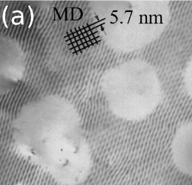
A completely different situation takes place in the EuS/PbTe superlattices. Here, due to the very large misfit, the critical thickness is so small that only one monolayer of the material (EuS or PbTe) can be grown pseudomorphically on the other. Thus, in the case of EuS/PbTe SL’s one never can obtain a pseudomorphic system – instead, after the first monolayer is deposited, the growth proceeds in the Stransky-Krastanov mode. The deposition process produces not a continuous layer, but separate islands. In each such island relatively short-range edge misfit dislocation grids are formed, as shown in Figure 6(a).
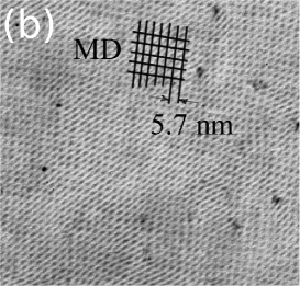
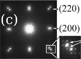
As the thickness of the deposited layer increases, the islands coalesce. A continuous layer is formed and the misfit dislocations order into a long range periodic grid at the interface between the two layers. The periodicity of the grid is inversly proportional to the misfit parameter and equals 57 Å for EuS/PbTe. An example of such a grid formed in a EuS/PbTe bilayer can be seen in in the electron microscope image presented in Figure 6(b). And in Figure 6(c) an electron diffraction image from the same bilayer is presented, showing a number of superstructure reflections corresponding to the periodicity of the dislocation grid.
The dislocation grids release much of the misfit strain in the multilayer. The remaining unrelaxed strain is now sinusoidally modulated in two ortogonal directions in the plane of the interface. The distribution of the elastic deformation of the EuS lattice in the interface plane, is illustrated in Refs. [14, 15], (in Figures 10 and 5, respectively).
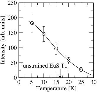
One can expect that the presence of such dislocation grids in the EuS layers may give rise to highly interesting magnetic phenomena. The sinusoidally modulated strain exerts alternating compresive and tensile pressure on the magnetic material near the interfaces. Further away from the interface regions, in the middle of the layer, the influence of the interfacial strain may be greatly reduced (see Figure 5 in [15]) leaving that portion of the EuS layer essentially unchanged. The actual strain distribution depends on the lattice misfit and on the thicknesses of both, magnetic and nonmagnetic, layers [15, 16]. Neutron diffraction under sufficiently high hydrostatic pressure has shown that the Curie temperature of EuS is very sensitive to the applied pressure. A pressure of 20 GPa shifts the EuS from 16.6 K to about 150 K [17]. The peak value of the interplanar distance modulation due to 8% lattice misfit between EuS and PbTe in a multilayer system is equivalent to an applied uniaxial pressure of about 25 GPa. Consequently, the near-interface areas of the EuS layer that experience compresive strain should stay magnetically ordered at temperatures considerably higher than the Curie point of an unstrained EuS layer. By the same token, the-near interface portions of the EuS layer which are under tensile strain should remain magnetically disordered at temperatures well below the of unstrained EuS.
5 Polarized neutron reflectivity investigation of EuS/PbTe
Our attempts to directly demonstrate the magnetization modulation by magnetic neutron diffraction measurements have so far been unsuccessful. A possible reason may be the relatively low volume of the stress modulated EuS. A significant modulation may only be confined to relatively small portions of the EuS layers in the vicinity of the PbTe-EuS interfaces – which results in a very low diffracted intensity. Below larger, unmodulated part of the layer plays a dominant role, masking the much weaker signal produced by the smaller modulated part on the diffracted intensity. Above the main, unmodulated, part of the layer becomes magnetically disordered, and only the most compressed regions still remain magnetically ordered, forming a regular array of “nanomagnets”. It does not appears likely that such "nanomagnets" can interact with each other across the unmagnetized regions separating them. Therefore, in order to observe coherent magnetic diffraction from the array one should apply a sufficiently strong magnetic field that would allign all the magntization vectors in individual “nanomagnets”.
However, even in such circumstances the detection of a magnetic diffraction signal from the array poses a substantial challenge because this maximum occurs at the same position as the overwhelmingly stronger nuclear Bragg peak from the SL structure. Fortunately, the technique of polarized neutron diffraction offers the possibility to extract small magnetic signals superimposed on strong nuclear diffraction maxima. In brief, this method is based on the fact that for non-spin-flip scattering of a polarized neutron beam from a magnetized ferromagnet, the magnetic and the nuclear scattering components interfere – either constructively or destructively, depending on whether the neutron spins are parallel, or antiparallel to the sample magnetization vector. The difference between the intensities observed in these two scattering modes – which are conventionally denoted as and is proportional to the sample magnetization.
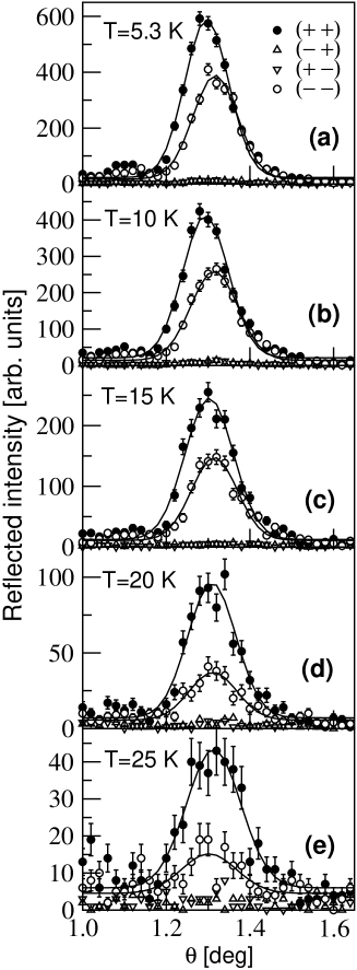
Figure 7 presents the results of polarization analysis applied to the 1st order SL Bragg peak from the EuS/PbTe (50/50) Å superlattice. The sample was placed in an applied magnetic field of 0.5 Tesla. All four scattering processes, the two non-spin-flip and , and the two spin-flip and have been measured. (The NIST NG-1 cold neutron reflectometer in polarized mode of operation was used.) As can be seen from the Figure 7, the very low and flat spin-flip, and , intensities prove that the sample is in a saturated state, with no transverse components of the magnetization.
The difference between the non-spin-flip, and , intensities is proportional to the sample magnetization [18]. In Figure 8 the difference between and intensities is plotted vs. temperature. As can be seen from Figure 7(d)–(e) and Figure 8, the magnetic contribution to the scattering persists well above the Curie point of the unstrained EuS (16.6 K).
6 Summary
In this paper the trends in interlayer coupling for two EuS-based families of all-semiconductor superlattices were investigated.
In one group of the studied SL’s, EuS/PbS, EuS/YbSe, and EuS/SrS, the nonmagnetic spacer materials are very well lattice matched (the misfit ) to EuS. Due to the very small , and consequently large , the layers in all these superlattices grow pseudomorphically and are negligibly stretched/expanded and have no dislocation grids formed on the interfaces. As a result, the EuS layers are magnetized uniformly, without modulation in the interface vicinity. The energy-gap of these spacers systematically increases from about 0.3 eV for narrow-gap PbS, through 1.6 eV for wide-gap YbSe, to about 4 eV for insulating SrS. The experimentally observed strength of the interlayer coupling in this series of SL’s decreases monotonically as the energy gap of the spacer increases. These findings strongly support the prediction of the tight-binding calculations by Blinowski and Kacman [5, 6].
In the other group of studied SL’s, EuS/PbS, EuS/PbSe, and Eus/PbTe, all the spacers are narrow gap semiconductors with an energy gap of the order of 0.2 - 0.3 eV and have lattice misfits to EuS which monotonically increase from about 0.5% for PbS through 2.5% for PbSe to about 8% for PbTe. Although, the EuS/PbS and EuS/PbSe systems are both pseudomorphic, the considerably higher tensile strain of EuS in EuS/PbSe SL’s leads to a noticible decrease of the IC strength in the latter system as compared with EuS/PbS SL’s. In EuS/PbTe no AFM IC was observed, most likely due to the drastic modifications of the EuS magnetic properties around the interfaces. In addition, Stransky-Krastanov, island-like, growth of the layers contribute to the increased roughness of the interfaces and, very likely, discontinuities or pin-holes in the thinner PbTe spacers. The latter may be responsible for the weak ferromagnetic interlayer coupling, due to the direct contact between adjacent EuS layers, seen in some EuS/PbTe SL samples.
An enhanced EuS in EuS/PbTe superlattices has been found by neutron polarization analysis performed, on the first-order SL Bragg peak, in a saturating magnetic field. The origin of this enhancement was attributed to the existence of highly compressed EuS regions in the vicinity of EuS-PbTe interfaces due to the misfit dislocation grid in EuS/PbTe system.
References
References
- [1] P. Wachter, Europium chalcogenides: EuO, EuS, EuSe and EuTe, in Handbook on the Physics and Chemistry of Rare Earth, edited by K. A. Gschneider and L. R. Eyring, volume 2, pages 507–574, North Holland, Amsterdam, 1979.
- [2] H. Kępa et al., Europhys. Lett. 56, 54 (2001).
- [3] H. Kępa, C. F. Majkrzak, P. Sankowski, A. Y. Sipatov, and T. M. Giebultowicz, J. Alloys and Compounds 401, 238 (2006).
- [4] P. Bruno, Phys. Rev. B 52, 411 (1995).
- [5] J. Blinowski and P. Kacman, Phys. Rev. B 64, 045302 (2001).
- [6] P. Sankowski and P. Kacman, Acta Phys. Polon. A 103, 621 (2003).
- [7] M. Szot et al., Acta Phys. Polon. A 112, 419 (2007).
- [8] P. Sankowski et al., Acta Phys. Polon. A 105, 607 (2004).
- [9] I. V. Markov, Crystal Growth for Beginners: Fundamentals of Nucleation, Crystal Growth, and Epitaxy, World Scientific, Singapore, 2003.
- [10] J. Venables, Introduction to Surface and Thin Film Processes, Cambridge University Press, Cambridge, 2000.
- [11] S. Jain, M. Willander, and R. V. Overstraeten, editors, Compound Semiconductors Strained Layers and Devices, Kluver, Boston, 2000.
- [12] A. Stachow-Wójcik et al., Phys. Rev. B 60, 15220 (1999).
- [13] T. Story, physica status solidi (b) 236, 310 (2003).
- [14] N. Y. Fogel et al., Phys. Rev. B 66, 174513 (2002).
- [15] I. F. Mikhailov, B. A. Savitskii, A. Y. Sipatov, A. I. Fedorenko, and L. P. Shpakovskaya, Sov. Phys. Solid State 25, 668 (1983).
- [16] A. I. Fedorenko, B. A. Savitskii, A. Y. Sipatov, and L. I. Shpakovskaya, Sov. Phys. Crystallogr. 27, 569 (1982).
- [17] I. N. Goncharenko and I. Mirebeau, Phys. Rev. Lett. 80, 1082 (1998).
- [18] R. M. Moon, T. Riste, and W. C. Koehler, Phys. Rev. 181, 920 (1969).