Highly transparent superconducting – normal junctions in a homogeneous superconductor induced by local fields of magnetic domains
Abstract
Using the highly inhomogeneous fields of a magnetic substrate, tunable junctions between superconducting and normal state regions were created inside a thin film superconductor. The investigation of these junctions, created in the same material, gave evidence for the occurrence of Andreev reflection, indicating the high transparency of interfaces between superconducting and normal state regions. For the realization of this study, a ferromagnet with magnetic stripe domains was used as a substrate, on top of which a superconducting transport bridge was prepared perpendicular to the underlying domains. The particular choice of materials allowed to restrict the nucleation of superconductivity to regions above either reverse-domains or domain walls. Moreover, due to the specific design of the sample, transport currents in the superconductor passed through a sequence of normal and superconducting regions.
pacs:
74.45.+c, 75.60.Ch, 74.78.DbI Introduction
There is a wealth of physical phenomena inherent to junctions between superconducting (S) and normal (N) matter, such as the Josephson effect Josephson:1974 , quasi-particle tunneling Meservey:1970 and Andreev reflection (AR) Andreev:1964 . Traditionally, SN junctions are either based on composites of superconducting and normal-conducting materials, or on constrictions/thickness modulations of superconducting films. A common feature of these junctions is their fixed character, since they are static constructions that can not be modified any more once they are fabricated. However, recent works have shown that the highly inhomogeneous fields of ferromagnetic domains can be used to locally suppress superconductivity in thin S-films, resulting in the states of domain-wall superconductivity Yang:2004 (DWS) or reverse-domain superconductivity Fritzsche:2006 (RDS). In these two states, the superconductor can be seen as a network of SN junctions, which can exhibit the same flexibility as the underlying magnetic domains. In this article, we demonstrate that tunable SN junctions can be created in a controlled way by using the highly inhomogeneous fields of ferromagnetic domains. In particular, we show that in such junctions, the interfaces between the superconducting and the normal parts are highly transparent for incident electrons, which is a consequence of creating superconducting and normal state regions inside the same material.
In order to experimentally investigate SN interfaces that are induced by stray magnetic fields, a specially designed superconductor/ferromagnet (S/F) hybrid Buzdin:2005 ; Lyuksyutov:2005 ; Aladyshkin:2009 system was needed, exhibiting the following two qualities: (i) The opportunity to specifically realize superconductivity either above the magnetic domain walls (DWS) or above the reverse domains (RDS) of the substrate. (ii) Transport currents had to cross effectively the interfaces between the induced superconducting and normal-state regions. The preparation of such system is challenging as several strict requirements need to be fulfilled. First of all, formation of magnetic stripe domains in the template is desirable Belkin:2008 . Alignment of a transport bridge perpendicular to such domains guarantees a bias current to cross them successively. Second, the magnetic domain pattern of the template must not change significantly when subjected to external fields, required for setting up the different states (e.g. RDS) in the S-layer. Finally, the out-of plane component of the stray field above magnetic domains has to reach the upper critical field of the superconductor Sonin:1988 . Thereby, realization of DWS is possible down to temperatures well below .
II Experimental
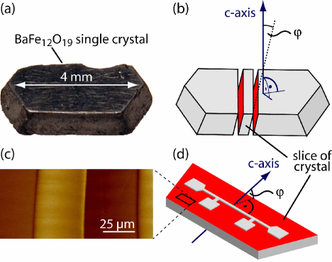
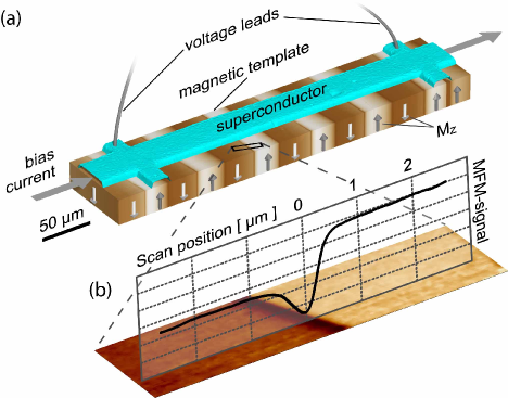
Accounting for the above requirements, S/F hybrid systems were prepared by slicing a single crystal of barium hexaferrite (BaFe12O19) under a small tilt to its c-axis (Figure 1(b)), and then processing superconducting aluminium bridges of 50 nm thickness on the cut surfaces perpendicular to the c-axis (Figure 1(d)). The superconducting and ferromagnetic components were electrically isolated by 5 nm SiO2 in order to prevent any proximity effect. The ferromagnetic crystal (Figure 1(a)) was grown from a sodium carbonate flux, following a recipe after Gambino:1961 . When cut along the proper crystallographic axis, single crystals of BaFe12O19 exhibit a one-dimensional stripe-type domain structure (Figure 1(c)) with dominant in-plane magnetization and relatively small out-of-plane component Hubert:403 .
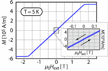
To demonstrate that these magnetic domains do not change significantly in perpendicular external magnetic fields mT, the magnetization of one slice of the single crystal was measured with a vibrating sample magnetrometer as a function of (see Figure 2). Apparently, the magnetization of the ferromagnet depends almost linearly on the perpendicular applied magnetic field and saturates at 1.7 T. From the slope Am-1T-1, one can indeed expect only minor changes of the domain structure for mT, since the corresponding variation of the magnetic moment is less than 7 of the saturated magnetization ( Am-1T-1).
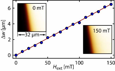
Furthermore, the influence of the external magnetic field on the size and position of the magnetic domains was studied at low-temperatures (77 K) with a scanning Hall-Probe microscope Bending:1999 . As it is shown in Figure 3, the width of the parallel domains increases linearly for mT with a rate of approximately 43 nm/mT. In accordance with the very small coercivity of these ferromagnets (see Figure 2), the observed domain walls returned to their initial positions within the experimental resolution of 1 m, each time was reduced to zero.
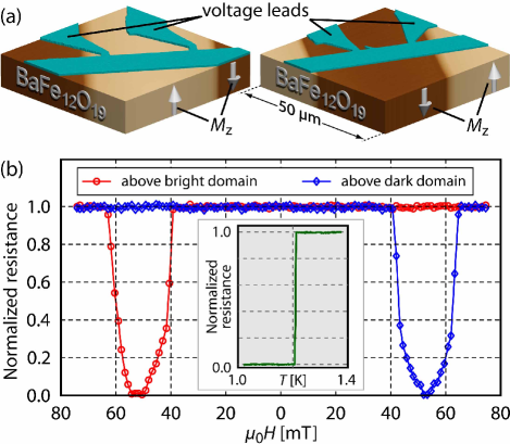
In order to show that the prepared S/F hybrid systems are suitable for the study of stray field induced SN interfaces, Figure 4(b) shows the normalized resistance ( being the normal state resistance) of two transport bridges as a function of . Both curves were measured at 340 mK, i.e. well below the critical temperature K of the used aluminum (see the insert of Figure 4). From the corresponding atomic and magnetic force microscopical images (AFM and MFM, respectively) of Figure 4(a), it can be seen that the measured parts of the bridges lay entirely above magnetic domains of opposite magnetization. The difference in the MFM signal above the two kinds of domains indicates a non-zero out-of plane component of the stray magnetic field. Note that above the wide domains results directly from a finite cutting angle to the c-axis of the crystal. Therefore, by choosing , the strength of can be adapted to match the critical fields of the superconductor. For the present case, it was found that aluminium as a superconductor and are a good match. For the case of the bridge above the bright domain (left panel of Figure 4(a)), drops to zero around -53 mT (see the red curve with circles). In a symmetric manner, of the bridge above the dark domain shows a similar behavior around +53 mT (see the blue curve with diamonds). These observations prove the possibility to realize the state of RDS by applying compensation fields of mT to the designed Al/BaFe12O19 hybrids. Moreover, it becomes clear that in the state of RDS at 340 mK, the superconducting order parameter is completely suppressed above the corresponding parallel domains (i.e. above magnetic domains with magnetization in the same direction as ).
Next, a long transport bridge of was investigated, which – due to its relatively large size – had to cross several magnetic domain walls of the substrate. Inspection of the sample with a magnetic force microscope revealed indeed nine domain walls underneath the bridge (Figure 5(a)). Figure 6 displays the normalized dc-resistance of the bridge well below , measured as a function of bias current and . As can be expected from the above presented results, two pronounced minima in resistivity are seen around mT, indicating that stray fields above magnetic domains are compensated by . Application of these compensation fields thus induces the RDS state in the S/F hybrid system. Furthermore, a second key feature can be seen in Figure 6. While beyond the compensation fields the resistance quickly rises towards its value in the normal state, parts of the bridge remain superconducting when subjected to external fields lower than the compensation fields. Particularly, in the case of zero applied field, when superconductivity is likewise suppressed above domains of opposite magnetization, the reduced resistance is a clear fingerprint of DWS. Moreover, the insert in Figure 6 shows the transitions of the bridge from the normal state to the states of DWS and RDS (at 0 mT and 53 mT, respectively) as a function of temperature. The significant difference of the onsets of the transitions reflects the confinement of the superconducting order parameter above wide magnetic domains (RDS) and narrow domain-walls (DWS) Aladyshkin:2006 .
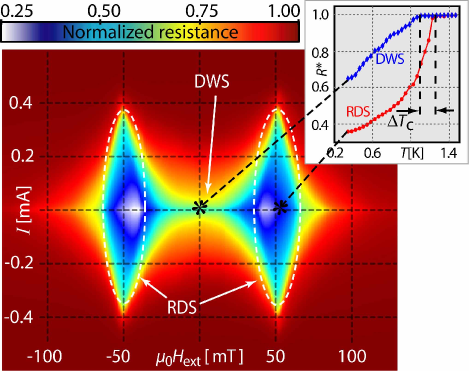
Above, the occurrence of the minima in Figure 6(a) has been discussed, along with the reduction of resistance at zero applied field. However, surprising are the values of the resistance reached at these points: As can be seen from Figure 5(a), approximately half of the area of the bridge is covered by each kind of domains. Nucleation of superconductivity above one type of domains should thus cause the bridge to loose roughly half of its resistance in the normal state. By contrast, for compensation fields of both polarities, only half of the expected resistance is seen.
A similar observation can be made at when superconductivity survives above domain walls only. In that case, the drop in resistance is, a priori, expected to be equal to the ratio between the width of magnetic domains and domain walls. But from detailed MFM studies it becomes clear that all changes in stray fields are confined to approximately 1 around domain walls (Figure 5(b)), whereas the domains are typically 25 wide (Figure 5(a)). Therefore, in absence of external fields, the observed reduction of resistance by % is surprising.
In order to investigate these remarkable features in more detail, the differential resistance of the transport bridge was measured as a function of bias current and temperature in both states, RDS and DWS. Simultaneously, the voltage drop over the bridge was also detected. Measurements were carried out via standard lock-in techniques at a frequency of 33 Hz and an ac-modulation current of 2 A. The normalized differential conductance is shown in Figure 7 as a function of voltage for mT (RDS). In that diagram, results are shown twice for clarity: the left 2D-panel displays a few conductance curves that are vertically shifted, whereas all obtained curves are given in a 3D-representation at the right. Here, at lowest temperatures, is sharply peaked at zero voltage, declining symmetrically to its minima at before recovering to its normal value at higher voltages. Together with some smaller local minima, these features gradually collapse with increasing temperature.
III Discussion
In order to interpret the conductance spectra of Figure 7, several aspects must be taken into account:
(i) The whole transport bridge is in the normal state for 2 mV even at the lowest temperature (340 mK). The reason for this is that the critical current density is exceeded due to the low resistance of the bridge. Therefore, in a certain low-voltage region where , a higher value for is expected, since the parts of the bridge above reverse-domains (RD) are superconducting.
(ii) The normalized differential conductance reaches 2.8 at 340 mK and zero voltage. Assuming that this increase of was solely caused by the N S transition mentioned under point (i), approximately 64% of the transport bridge had to become superconducting. However, the hybrid system behaves similar for both polarities of (see Figure 6), meaning that an unequal distribution of parallel and reverse domains can not be the reason for the high conductances observed at positive and negative compensation fields. Moreover, as discussed above, the external field increases the width of the parallel domains by 43 nm/mT (see Figure 3). Accordingly, at 53 mT, a normalized conductance of only 1.8 instead of 2 should be expected, provided that parallel and reverse domains are equally distributed at . Finally, the characteristic length , over which the Cooper pair amplitude decays exponentially with the distance from an SN interface, is in the present case of the order of 400 nm 111An estimation of the diffusion coefficient is m2/s, with the Fermi velocity m/s Ashcroft and the electron mean free path nm ( and are electronic mass and charge, m-3 is the density of conduction electrons Ashcroft ). The residual resistance was estimated according to , with the resistivity m of Al at 295 K Kittel .. Due to this proximity effect, the superconducting state extends into the normal regions and vice versa, but the corresponding increase of at is only minor.
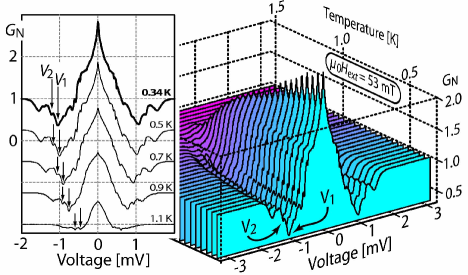
Taking account of the above considerations, the observed conductance of 2.8 can not be explained by a corresponding expansion of the superconducting state along the transport bridge. However, below the superconducting gap (i.e. for ), an excess of the conductance can generally result from Andreev reflection processes at SN-interfaces, if the latter are highly transparent for incident electrons. In the present case, normal and superconducting states are created inside the same material and, therefore, the presence of higly transparent SN-interfaces is reasonable. Accordingly, the observed excess of conductance suggests that the mechanism of charge transfer across the SN-interfaces is affected by AR.
The theory of Blonder, Tinkham and Klapwijk (BTK) Blonder:1982 describes the effects of AR on the conductance of a single SN junction for the particular case of ballistic transport in the normal-state region. From that theory it follows that inside the gap, the conductance can be enhanced up to twice its above-gap value. In the present case, as discussed above, the above-gap conductance in the RDS-state at 53 mT can be estimated to be 1.8. Therefore, the observed zero-voltage conductance of 2.8 is smaller than twice the above-gap conductance (), meaning that these findings are not in contradiction with the BTK-theory.
Moreover, the BTK-theory predicts for highly transparent interfaces a flat conductance below the gap, which has been verified experimentally with superconducting point contacts (see for example Soulen:1998 ). By contrast, the -curves of Figure 7 are sharply peaked at zero voltage. Such anomalies in the conductance spectra in the form of zero-bias peaks have been reported before in systems that deviate from the model of BTK, such as for example planar Nb/Au contacts Xiong:1993 , junctions between superconductors and semiconductors Kleinsasser:1990 ; Nguyen:1992 ; Kastalsky:1991 and series of SNS-junctions Kvon:2000 . In the present case, the used sample differs also significantly from the model system of BTK, since the bridge crosses nine domain walls (see Figure 5(a)), each of them inducing one SN interface. Moreover, due to the large size of the domains, the electric transport in the normal-state regions is not ballistic. A theoretical description of such series of diffusive SNS junctions will go beyond the ballistic theories Blonder:1982 ; Octavio:1983 , and will have to include nonlocal coherent effects in the normal-state regions Wees:1992 ; Nazarov:1996 .
(iii)
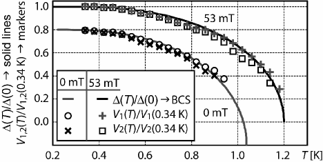
Two of the local minima of the conductance spectra of Figure 7, marked as and , can be traced from 340 mK to nearly . Their relative position on the -axis was compared to the superconducting gap function
of the BCS-theory Tinkham:63 , using a value of 423 K for the ratio between cut-off frequency and Boltzmann constant Gschneidner:1964 . A solution of the above equation can be found by iteration, integrating numerically over energies while treating as a fitting parameter. As illustrated in Figure 8 (upper curve), follow strictly the superconducting gap in temperature.
For the ideal case of a single ballistic SNS junction, it is known
that multiple Andreev reflection (MAR) leads to minima in the
conductance curves at voltages smaller than the gap
(). Their positions follow in the same way
as . However, the present case is quite different in that
the measured -curves belong to a series of diffusive SNS
junctions. When dividing by the number of SN
interfaces Baturina:2002 and considering that dropped
mainly over the normal-state regions of the bridge, it could be
concluded that lay inside the gap and originate from MAR
(typical values for are 200 V for
Al Giaever:1961 ). However, it is also possible that series
of AR processes lead to multiplication effects and to different
effective voltages across subsequent SN interfaces. Therefore,
even if caused by the same process, features in could
repeatedly appear at different voltages, and result in the
observed set of local minima. Moreover, a multiplication effect in
series of junctions might also lead to an increase of the
conduction by factors higher than two Shan:2003 .
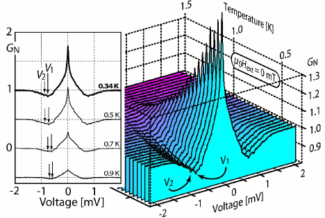
Intriguingly, all observations described above can be made not only in the case of RDS but also in absence of external fields when DWS is realized (Figure 9). In that case, local minima are less pronounced, but nonetheless, two of them can be traced up to higher temperatures (lower curve in Figure 8). As before, their positions in the conductance spectra follow the collapse of . It is remarkable that values of obtained by fitting are significantly different in the cases of RDS ( K) and DWS ( K). These findings reflect directly that due to quantum size effects, values of superconducting micro-structures differ significantly from those of bulk superconductors Moshchalkov:1995 – an effect that leads to the reduction of when superconductivity is confined above the domain walls of a underlying ferromagnet Gillijns:2007PRB76 .
IV Conclusions
In conclusion, there are two major findings of this work: On one hand, it has been demonstrated that tunable SN junctions inside superconducting thin films can be created in a controlled manner by using magnetic templates. This first conclusion is a direct result from the successful fabrication of a S/F hybrid system, that allows for setting up DWS and RDS in the S-layer, without changing the actual configuration of magnetic domains. On the other hand, the occurrence of Andreev reflection, observed in the conductance of the S-layer of the hybrid system, proves the high transparency of SN interfaces induced by magnetic stray fields. This result is based on the innovative approach to create SN junctions in the same material via local suppression of superconductivity.
From a technological point of view, generation of SN junctions via ferromagnets is attractive due to both, the natural tunability of magnetic domain structures and the here demonstrated high quality of SN interfaces. Potentially, inclusion of magnetic templates with pure in-plane magnetization will make it possible to invert the scheme of DWS and to suppress superconductivity in a very narrow region above domain walls, realizing the domain-wall normal state (DWN). Such configuration may lead to controllable phase coupling effects between two superconducting reservoirs, separated by a thin DWN region, and pave the way for the development of new types of tunable quantum interference devices.
Acknowledgements.
This work is supported by the FWO, GOA and IAP projects and the ESF-NES Research Networking Programme.References
- (1) B. D. Josephson, Rev. Mod. Phys. 46, 251 (1974).
- (2) R. Meservey, P. M. Tedrow and P. Fulde, Phys. Rev. Lett. 25, 1270 (1970).
- (3) A. F. Andreev, Sov. Phys. JETP 19, 1228 (1964).
- (4) Z. Yang, M. Lange, A. Volodin, R. Szymczak and V. V. Moshchalkov, Nature Mater. 3, 793 (2004).
- (5) J. Fritzsche, V. V. Moshchalkov, H. Eitel, D. Koelle, R. Kleiner and R. Szymczak, Phys. Rev. Lett. 96, 247003 (2006).
- (6) A. I. Buzdin, Rev. Mod. Phys. 77, 935 (2005).
- (7) I. F. Lyuksyutov and V. L. Pokrovsky, Adv. Phys. 77, 67 (2005).
- (8) A. Yu. Aladyshkin and A. V. Silhanek and W. Gillijns and V. V. Moshchalkov, Supercond. Sci. Technol. 22, 053001 (2009).
- (9) A. Belkin, V. Novosad, M. Iavarone, J. Fedor, J. E. Pearson, A. Petrean-Troncalli and G. Karapetrov, Appl. Phys. Lett. 93, 072510 (2008).
- (10) É. B. Sonin, Pis’ma Th. Tekh. Fiz. 14, 1640 (1988).
- (11) R. J. Gambino and F. Leonhard, J. Am. Ceram. Soc. 44, 221 (1961).
- (12) A. Hubert and R. Schäfer, Magnetic Domains, Springer-Verlag Berlin Heidelberg 1998, ch. 5, p. 403.
- (13) S. J. Bending, Adv. Phys. 48, 449 (1999).
- (14) A. Yu. Aladyshkin and V. V. Moshchalkov, Phys. Rev. B 74, 064503 (2006).
- (15) N. W. Ashcroft and N. D. Mermin, Solid State Physics , Brooks/Cole 1976, ch. 2, p. 38.
- (16) C. Kittel, Introduction to Solid State Physics, John Wiley & Sons Inc 1976, ch. 6, p. 171.
- (17) G. E. Blonder, M. Tinkham and T. M. Klapwijk, Phys. Rev. B 25, 4515 (1982).
- (18) R. J. Soulen Jr. and J. M. Byers and M. S. Osofsky and B. Nadgorny and T. Ambrose and S. F. Cheng and P. R. Broussard and C. T. Tanaka and J. Nowak and J. S. Moodera and A. Barry and J. M. D. Coey, Science 282, 85 (1998).
- (19) P. Xiong, G. Xiao and R. B. Laibowitz, Phys. Rev. Lett. 71, 1907 (1993).
- (20) A. W. Kleinsasser, T. N. Jackson, D. McInturff, F. Rammo, G. D. Pettit, Appl. Phys. Lett. 57, 1811 (1990).
- (21) C. Nguyen and H. Kroemer and E. L. Hu, Phys. Rev. Lett. 69, 2847 (1992).
- (22) A. Kastalsky and A. W. Kleinsasser and L. H. Greene and R. Bhat and F. P. Milliken and J. P. Harbison, Phys. Rev. Lett. 67, 3026 (1991).
- (23) Z. D. Kvon and T. I. Baturina and R. A. Donaton and M. R. Baklanov and K. Maex and E. B. Olshanetsky and A. E. Plotnikov and J. C. Portal, Phys. Rev. B 61, 11340 (2000).
- (24) M. Octavio, M. Tinkham, G. E. Blonder and T. M. Klapwijk, Phys. Rev. B 27, 6739 (1983).
- (25) B. J. van Wees, P. de Vries, P. Magnee and T. M. Klapwijk, Phys. Rev. Lett. 69, 510 (1992).
- (26) Yu. V. Nazarov and T. H. Stoof, Phys. Rev. Lett. 76, 823 (1996).
- (27) T. Tinkham, Introduction to Superconductivity, Dover, New York 1996, ch. 3, p. 63.
- (28) K. A. Gschneidner, Solid State Phys. 16, 275 (1964).
- (29) T. I. Baturina, D. R. Islamov and Z. D. Kvon, JETP 75, 326 (2002).
- (30) I. Giaever and K. Megerle, Phys. Rev. 122, 1101 (1961).
- (31) L. Shan, H. J. Tao, H. Gao, Z. Z. Li, Z. A. Ren, G. C. Che and H. H. Wen, Phys. Rev. B 68, 144510 (2003).
- (32) V. V. Moshchalkov, L. Gielen, C. Strunk, R. Jonckheere, X. Qiu, C. Van Haesendonck, and Y. Bruynseraede, Nature 373, 319 (1995).
- (33) W. Gillijns, A. Yu. Aladyshkin, A. V. Silhanek and V. V. Moshchalkov, Phys. Rev. B 76, 060503(R) (2007).