Picovoltmeter for probing vortex dynamics in a single weak-pinning Corbino channel
Abstract
We have developed a picovoltmeter using a Nb dc Superconducting QUantum Interference Device (SQUID) for measuring the flux-flow voltage from a small number of vortices moving through a submicron weak-pinning superconducting channel. We have applied this picovoltmeter to measure the vortex response in a single channel arranged in a circle on a Corbino disk geometry. The circular channel allows the vortices to follow closed orbits without encountering any sample edges, thus eliminating the influence of entry barriers.
I Introduction
The dynamics of vortices in confined superconductor geometries has generated much interest in recent years, with studies of both fundamental properties of vortex matter as well as devices based on the motion of vortices. Nanoscale channels for guiding vortices through superconducting films with a minimal influence from pinning have been developed for explorations of vortex melting Besseling et al. (2003), commensurability Pruymboom et al. (1988), mode locking Kokubo et al. (2002), and ratchets Yu et al. (2007). These channels are typically arranged across the width of a superconducting strip, so that the vortices enter the channel at one edge of the strip and exit at the other edge, resulting in edge barriers to the vortex motion through the channels Vodolazov and Maksimov (2000); Plourde et al. (2001); Benkraouda and Clem (1998). The strip geometry also allows for the use of multiple channel copies in parallel to boost the flux-flow signal strength for measurement with a room-temperature amplifier.
It is possible to eliminate the edge barriers characteristic of a strip arrangement by using a Corbino geometry, consisting of a superconducting disk, with current injected radially between the center and the perimeter. Vortices in such a disk experience an azimuthal Lorentz force and can flow in closed circular orbits without crossing any edges. The Corbino geometry has been used for many studies of vortex matter in different superconductors, including bulk crystals of YBCO López et al. (1999) and NbSe2 Paltiel et al. (2000). We have patterned thin-film Corbino disks with submicron circular channels for probing vortex dynamics in a narrow region free from edge barriers. Because the current density decreases radially in a Corbino geometry, such that vortices at different radii experience a different Lorentz force Babaei Brojeny and Clem (2001), we have designed our devices to have only a single channel. This poses a challenge for the amplifier used to detect the vortex motion. In this article, we present a scheme for driving a small number of vortices through a single, circular submicron channel and a picovoltmeter for resolving the ensuing flux-flow voltages.
II Channel fabrication
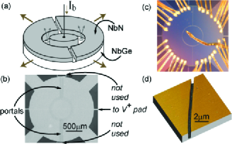
We fabricate our channels from bilayers of nm-thick films of amorphous-NbGe, an extremely weak-pinning superconductor ( K), and nm-thick films of NbN, with relatively strong pinning ( K), on a Si substrate. After patterning and etching a mm-diameter Corbino disk into such a bilayer, we define a nm-wide channel in a circle with a m diameter using electron beam lithography (Fig. 1). We etch this region down to a depth of nm using a reactive ion etch with CF4, thus completely removing the NbN in this region and etching partially into the NbGe layer. In addition to the circular channel, we etch two radial channels (portals) that extend from opposite sides of the circular channel out to the edge of the Corbino disk. These portals allow for the introduction of vortices into the channel by field-cooling from temperatures , as they break up the circulating supercurrent in the outer NbN region.

We attach leads for driving the bias current through the Corbino disk using mil Al wirebonds, with bonds around the perimeter of the disk. The connection to the center consists of a superconducting Nb wirebond using annealed mil Nb wire [Fig. 1(c)]. The azimuthal Lorentz force from causes the vortices to flow around the channel when this force exceeds the residual pinning in the NbGe channel. The ensuing vortex dynamics in the channel can be characterized by measuring the radial voltage drop across the channel, , which is proportional to the vortex velocity and density.
III Picovoltmeter design and characterization
The flux-flow voltage for vortices moving in a single channel at a low velocity can be quite small. For example, vortices with a density corresponding to a magnetic induction of G in the channel moving at a velocity of m/s, less than one percent of the typical Larkin-Ovchinnikov instability velocity for NbGe Larkin and Ovchinnikov (1975); Babić et al. (2004), produce a flux-flow voltage of pV. In order to resolve such signals, we have developed a voltmeter, based on a Nb dc SQUID, which we obtained from ez SQUID. Sensitive voltmeters were one of the original applications of SQUIDs Clarke (1966), and SQUID voltmeters have been used previously to probe the nature of the vortex state in bulk crystals of YBCO Gammel et al. (1991) and BSCCO Safar et al. (1992). To the best of our knowledge, our scheme is the first application of a dc SQUID to form a picovoltmeter for resolving vortex dynamics in a patterned thin-film structure, as well as in a Corbino geometry.

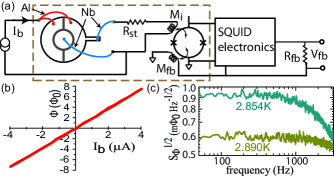
We connect the voltage leads across the NbGe channel to the SQUID input coil with a resistor, , consisting of a segment of brass foil ( x x mm3). This converts the flux-flow voltage to a current through the input coil, which has a self inductance and a mutual inductance to the SQUID [Fig. 2(a)]. Except for , all of the voltage connections are superconducting. We make the voltage contacts on the Corbino disk with Nb wirebonds, where the connection shares the superconducting Nb wire to the center of the Corbino disk with the connection, while the Nb wirebond is attached to a pad of the NbGe/NbN bilayer that extends from the perimeter of the Corbino disk [Fig. 1(b)]. The other ends of these Nb wirebonds are attached to superconducting solder-tinned copper traces on our chip carrier using Pb washers. The connection is soldered to , then the traces are attached to a twisted pair of mil Nb wire with a second set of screw terminals using Pb washers. Finally, this Nb twisted pair is coupled to the input circuit on the SQUID holder with superconducting screw terminals.
We operate the SQUID in a conventional flux-locked loop, using a MHz electronics system from ez SQUID, with the feedback signal supplied through a feedback resistor to a wire-wound coil with a mutual inductance to the SQUID. The SQUID holder is mounted in a Nb cylindrical shield that is closed on one end. The entire bottom end of the experimental insert is enclosed in a Pb cylindrical shield, and the dewar is surrounded by a -metal shield that is closed on the bottom.
A simple circuit analysis leads to the following expression relating to the voltage across the channel :
| (1) |
The ratio can be obtained in the usual way by measuring the difference in with the SQUID locked in adjacent wells ( mV), and was measured to be nH through a separate calibration. We estimate to be m based on the size of the brass foil, but we can obtain a more careful calibration of the voltmeter gain through a series of low-temperature measurements. We first measure the current-voltage characteristic of the Corbino channel at K, where the NbGe channel is in the normal state, while the NbN banks are superconducting. Figure 2(b) shows the flux coupled to the SQUID plotted against the bias current , which was monitored by tracking the voltage drop across a room-temperature current-sensing resistor. Because the channel is in the normal state, divides between the channel, with resistance , and the SQUID input coil with series resistance . Based on K measurements of similar NbGe channels of various geometries, we estimate for this Corbino disk to be m.
The flux noise at and zero field is essentially white with a high-frequency roll-off determined by and the relevant resistance in the voltmeter circuit. By comparing the flux noise below this roll-off for temperatures above and below , we can obtain measurements of both and . Above , the flux noise is determined by the Nyquist noise current generated by flowing through , while for , the only resistance is [Fig. 2(c)]. In both cases the flux noise is more than an order of magnitude larger than the intrinsic flux noise for the SQUID, at Hz and K from a separate measurement with the voltmeter circuit disconnected from the input coil. This analysis leads to m and m, consistent with our rough estimates. In addition, the location of the flux noise roll-off corresponds to nH, consistent with the design of the input coil on this particular SQUID.
Applying our measured circuit and SQUID parameters with Eq. 1 yields a gain of . The measured flux noise at K can be referred back as a voltage noise across the Corbino channel of pV/Hz1/2. Integrating over the kHz bandwidth of the voltmeter yields an rms noise level of pV. Of course, this noise could be reduced further, simply by using a smaller value of , with a concomitant reduction in the measurement bandwidth.
IV Measurements of Flux-Flow in Corbino Channel with Picovoltmeter
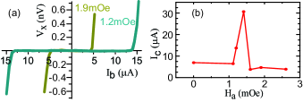
We have applied our voltmeter to measure the current-voltage characteristics (IVCs) of our single Corbino channel at K for several different cooling fields . During our measurements, the Corbino disk and SQUID circuitry are immersed in a pumped helium bath. For each value of , the insert was raised just above the bath and heated to K, above , and was then cooled in , generated with a superconducting coil. We recorded and with a digital oscilloscope, taking averages per point. The IVCs [Fig. 3(a)] exhibit a zero-voltage region at small followed by an increasing flux-flow voltage for beyond a depinning critical current . Using a voltage criterion of pV, we extract , which has a peak around mOe. This peak points to zero absolute field, or the limit of no vortices trapped in the channel. In contrast to a superconducting strip, which has a moderate critical current even in zero applied field corresponding to the entry of vortices and anti-vortices at the strip edges from the self-field of the strip Vodolazov and Maksimov (2000); Benkraouda and Clem (1998), the Corbino disk should have a large critical current when no vortices are present, as in this case would correspond to the breakdown of superconductivity in the entire disk.

While the values of in our measurements are rather small, the intermediate field-cooling scheme generates substantial flux-focusing effects into the NbGe channel due to the superconducting NbN. A rough estimate, considering screening currents around the central disk of NbN inside the channel, and along the outer NbN banks Clem and Sanchez (1994); Vodolazov and Maksimov (2000), indicates the enhancement of may be of the order of x . Thus, cooling in an absolute applied field of mOe should nucleate at least vortices in the channel, where the effective area includes not only the channel, but the penetration of the vortex circulating currents into the NbN banks as well. A more detailed treatment of this flux focusing in the channels is beyond the scope of this paper.
Our measurements presented here have been performed close to , where the residual pinning in the channels was especially weak. This was necessary because of our wiring configuration, where the lead was shared with the connection to the center of the Corbino disk along a superconducting Nb wirebond. This Nb wirebond had a somewhat small critical current, thus requiring us to operate at temperatures where was below the Nb wirebond critical current. In future Corbino measurements, it should be possible to separate these leads attached to the center of the disk, with the Nb wirebond used only for the SQUID input connection, which does not need to sustain large currents because of the presence of , with separate Al wirebonds for the connection, which does not need to be superconducting.
In summary, we have demonstrated a SQUID picovoltmeter circuit for resolving vortex dynamics in a single, weak-pinning superconducting channel in a Corbino geometry. This technique will be useful for investigations of small numbers of vortices moving at low velocities in nanofabricated structures, such as vortex ratchets.
ACKNOWLEDGMENTS
We thank R. McDermott and M. Mück for stimulating discussions. This work was supported by the National Science Foundation under Grant DMR-0547147. We acknowledge use of the Cornell NanoScale Facility, a member of the National Nanotechnology Infrastructure Network, which is supported by the National Science Foundation (Grant ECS-0335765).
References
- Besseling et al. (2003) R. Besseling, N. Kokubo, and P. H. Kes, Phys. Rev. Lett. 91, 177002 (2003).
- Pruymboom et al. (1988) A. Pruymboom, P. H. Kes, E. van der Drift, and S. Radelaar, Phys. Rev. Lett. 60, 1430 (1988).
- Kokubo et al. (2002) N. Kokubo, R. Besseling, V. Vinokur, and P. H. Kes, Phys. Rev. Lett. 88, 247004 (2002).
- Yu et al. (2007) K. Yu, T. W. Heitmann, C. Song, M. P. DeFeo, B. L. T. Plourde, M. B. S. Hesselberth, and P. H. Kes, Phys. Rev. B 76, 220507 (2007).
- Vodolazov and Maksimov (2000) D. Y. Vodolazov and I. L. Maksimov, Physica C 349, 125 (2000).
- Plourde et al. (2001) B. L. T. Plourde, D. J. Van Harlingen, D. Y. Vodolazov, R. Besseling, M. B. S. Hesselberth, and P. H. Kes, Phys. Rev. B 64, 014503 (2001).
- Benkraouda and Clem (1998) M. Benkraouda and J. R. Clem, Phys. Rev. B 58, 15103 (1998).
- López et al. (1999) D. López, W. Kwok, H. Safar, R. Olsson, A. Petrean, L. Paulius, and G. Crabtree, Phys. Rev. Lett. 82, 1277 (1999).
- Paltiel et al. (2000) Y. Paltiel, E. Zeldov, Y. Myasoedov, M. L. Rappaport, G. Jung, S. Bhattacharya, M. J. Higgins, Z. L. Xiao, E. Y. Andrei, P. L. Gammel, et al., Phys. Rev. Lett. 85, 3712 (2000).
- Babaei Brojeny and Clem (2001) A. A. Babaei Brojeny and J. R. Clem, Phys. Rev. B 64, 184507 (2001).
- Larkin and Ovchinnikov (1975) A. I. Larkin and Y. N. Ovchinnikov, Zh. Eksp. Teor. Fiz. 68, 1915 (1975).
- Babić et al. (2004) D. Babić, J. Bentner, C. Sürgers, and C. Strunk, Phys. Rev. B 69, 92510 (2004).
- Clarke (1966) J. Clarke, Philosophical Magazine 13, 115 (1966).
- Gammel et al. (1991) P. L. Gammel, L. F. Schneemeyer, and D. J. Bishop, Phys. Rev. Lett. 66, 953 (1991).
- Safar et al. (1992) H. Safar, P. L. Gammel, D. J. Bishop, D. B. Mitzi, and A. Kapitulnik, Phys. Rev. Lett. 68, 2672 (1992).
- Clem and Sanchez (1994) J. R. Clem and A. Sanchez, Phys. Rev. B 50, 9355 (1994).