Size Dependence of Current Spin Polarization Through Superconductor/Ferromagnet Nanocontacts
Abstract
The spin polarization of the transport current through the interface between superconducting Al and ferromagnetic Fe is determined by means of Andreev reflection at nanostructured point contacts. We observe a systematic decrease of with decreasing contact resistance. Our data provide evidence for the reduction of by spin-orbit scattering and thus establish a link between density-of-states and transport spin polarizations.
pacs:
74.45.+c, 72.25.-b, 73.63.RtThe spin-dependent electronic transport in magnetic heterostructures is an emergent field because of potential applications in spintronics zut04 ; par04 . The knowledge of the current spin polarization of materials is a key issue for the functionality pri95 . This is particularly important for high- materials such as half-metallic alloys, e. g., Heusler compounds gal05 ; wur06 . The spin polarization of ferromagnets can be measured by various techniques, including spin-polarized photoemission joh97 , spin-dependent electron tunneling mes94 , and point-contact Andreev reflection (AR) between a ferromagnet F and a superconductor S jon95 . An issue of considerable importance is how the current spin polarization obtained by AR and64 is related to the ferromagnet’s bulk spin polarization xia02 .
AR has been widely used to extract the current spin polarization in a variety of materials sou98 ; upa98 ; nad00 ; ji01 ; ray03 ; par02 . In particular, Upadhyay et al. upa98 employed the type of contacts also used by us. AR at an interface between a normal metal N and S is the coherent process by which an electron from N incident on S is retro-reflected as a hole, thus creating a Cooper pair in S. The theoretical analysis of these experiments is usually carried out in the spirit of the Blonder-Tinkham-Klapwijk (BTK) theory blo82 . The ordinary reflection at the N/S interface is parametrized by a phenomenological parameter . The sensitivity of the Andreev process to the spin of the carriers originates from the spin content of a Cooper pair ( in conventional superconductors) and the conservation of the spin direction at the interface. Employing a ferromagnet as the nonsuperconducting electrode leads to a reduction of the AR probability for spin-singlet superconductors because incoming electron and outgoing hole must have opposite spins jon95 . Two major approaches have been suggested to extract from AR datas: (i) the AR current is decomposed into a fully spin-polarized and fully unpolarized current xia02 ; maz01 ; woo04 , (ii) spin-dependent transmission coefficients and are introduced, hence per04 . For a comprehensive recent review of different models to extract the AR spin polarization, see Ref. cha07, . In this letter, we report on AR spectra obtained on a series of nanostructured Al/Fe contacts that show a distinct dependence on contact size. A possible origin of this systematic size dependence is spin-orbit scattering, shedding light on the origin of the differences in the spin polarization determined by different experimental methods. We chose Fe in this work because it does not show surface degradation of when prepared under UHV, in contrast to many Heusler compounds that show a reduced at the surface.
We employ nanostructured Al/Fe point contacts (PCs) that are formed by two metal films connected by a tiny hole in an insulating membrane in between ral89 . These contacts are very stable and reproducible spectra are obtained even after several thermal cycles. Furthermore, in-situ preparation of the metal films in a single run avoids oxidation or degradation of the interface between the two electrodes. Holes of radius between 7.5 and 25 nm were fabricated by e-beam structuring of a 50-nm thick Si3N4. was determined from the contact resistance (see below) after evaporation in UHV of a 200-nm thick Al layer on the side of the membrane with a bowl-like funnel towards the hole, and of a 12-nm thick Fe layer topped by a Cu layer of thickness nm on the opposite (flat) side (see Refs. ral89, ; per04, for details). By variation of the process parameters for the e-beam lithographical prestructuring and subsequent reactive ion-etching, contacts with resistance between and are obtained. Low-ohmic PCs () implying a large contact diameter usually show clear evidence of non-ballistic transport and therefore were not used for the present investigation. The differential conductance vs. applied bias voltage was measured in a dilution refrigerator between mK and 2 K.
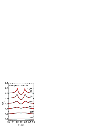
Fig. 1 exemplarily shows the differential conductance of a PC with at various temperatures below of the Al film. is normalized to the normal-state conductance . The data are analyzed in terms of two spin-dependent transmission coefficients and for the majority and minority charge carriers in F, respectively. We assume that the PC can be described with a single pair of transmission coefficients mar01 ; per04 which contain the microscopic properties relevant for the transport, i. e., the spin-split band structure of F, the electronic structure of S, and the interface properties. For , an electron experiences ordinary reflection with a finite probability . This leads to a minimum of at zero bias and sharp maxima at voltages corresponding to the superconducting energy gap . Using , , and as free parameters for each , the model yields excellent least-squares fits to the Andreev spectra over the whole range below and the entire voltage range, as shown in Fig. 1. Only at the lowest nominal mK, where the fit yields , , and eV, can the fits be distinguished from the data, the calculated maxima appear somewhat sharper than experimentally observed. This might be caused by a levelling-off of the electron due to heating by electromagnetic stray fields or a small pair-breaking effect by Fe. The excellent agreement between experiment and theory is also reflected in the dependence of the zero-bias resistance shown in Fig. 3a. is found to be 0.482 for this particular sample. The characteristic parameters for a total of six contacts are listed in Table 1.
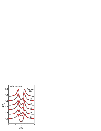
Shown in Fig. 2 are curves obtained at K for all samples. One clearly sees a systematic reduction of the amplitude of the AR-related features when going from sample 1 (small ) to sample 6 (large ), indicating a systematic increase of .Again, the quality of the fits is excellent over the whole voltage range up to .
| Sample | |||||||
|---|---|---|---|---|---|---|---|
| No. | (nm) | (meV) | (mK) | ||||
| 1 | 2.68 | 24.7 | 0.174 | 971 | 0.371 | 0.983 | 0.452 |
| 2 | 6.98 | 14.3 | 0.175 | 903 | 0.362 | 0.984 | 0.460 |
| 3 | 7.29 | 13.9 | 0.157 | 1009 | 0.349 | 0.993 | 0.480 |
| 4 | 9.59 | 12.0 | 0.190 | 970 | 0.361 | 0.984 | 0.462 |
| 5 | 18.4 | 8.4 | 0.166 | 1174 | 0.348 | 0.997 | 0.482 |
| 6 | 24.2 | 7.3 | 0.174 | 1115 | 0.343 | 0.994 | 0.487 |
The high stability of our PCs, together with the high quality of the fits, allows a detailed investigation of the dependence of and as displayed in Fig. 3b and 3c. is normalized to the experimental of each sample in order to account for the minor variation of from sample to sample. has been determined from the sudden drop of the zero-bias resistance (see Fig. 3a). follows the standard BCS dependence (solid line in Fig. 3b). At first sight, this might be surprising because the superconductor is in direct contact with a ferromagnet. Apparently, pair breaking plays a minor role as also inferred from the small rounding of the AR spectra mentioned above. Here, the small dimensions of the S/F contact are instrumental, because they limit the AR laterally to a tiny region and thus do not strongly affect S. Indeed, appears to be somewhat lower for low , i. e., larger contacts (see Table 1). The current spin polarization for each sample is independent of within the error of the least-squares fitting procedure (Fig. 3c). Only close to where the spectra become very shallow does the scatter in increase. The finding that is independent of strongly supports our assignment of as an intrinsic parameter of the particular S/F PC under study.
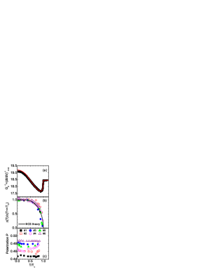
Inspection of Table 1 reveals that indeed depends on in a systematic fashion, i.e., larger contact resistances go along with larger . We interpret this finding as follows. In view of the fact that all samples were prepared in the same fashion, we are confident that it is chiefly the contact radius that determines . In particular, we recall that the interface between Al and Fe was never exposed to air. The radius of a circular homocontact can be calculated from for different regimes of current flow through the contact, depending on the ratio of to the electron mean free path of the material, with the limiting cases of the ballistic or Sharvin regime if and the thermal or Maxwell regime if . For the intermediate regime an interpolation for was suggested by Wexler wex66 . Here is a slowly varying function of with and and the Maxwell () and Sharvin limits () are given by and sha65 , respectively. Using arithmetically averaged parameters and m rem1 , and solving the Wexler formula iteratively for self-consistent values of , is found to vary between 7.3 and 24.7 nm, i.e., the change in corresponds to a change in by a factor of 3 (see Table 1).
decreases systematically as displayed in Fig. 4. The error bars reflect the statistical error of typically 6-8 measurements, all taken below 200 mK for each sample. We note that the overall trend of does not depend on the details of how was calculated. A possible explanation of the dependence is as follows. For large the incident electrons probe a larger volume before being retro-reflected as a hole than for a small . Any scattering process affecting will therefore have a stronger effect for larger contacts nai04 . We suggest that spin-orbit scattering with a constant scattering length is operative as the main source of the reduction of , and model the dependence by a simple exponential decay, . We obtain a spin-orbit scattering length nm from a fit to the data in Fig. 4. This value is very reasonable albeit somewhat lower than the spin diffusion length - 1000 nm found for Al bec04 , which – apart from the error introduced by the scatter of the data – may be attributed to a smaller elastic mean free path of our Al films or minor interdiffusion at the Al/Fe interface bra06 . We note that using the model of Mazin et al. maz01 with the fit parameters , , and , the same systematic trend of with even smaller is obtained with no systematic correlation between and . With this interpretation, our data constitute the first instance of a clear relation between the spin polarization of the Andreev current and the bulk spin polarization. almost reaches the value obtained by spin-polarized photoemission spectroscopy on polycrystalline Fe films bus71 and on the surface of single-crystalline Fe eib78 yielding and , respectively. The domain structure of the Fe film is expected to play no appreciable role for our PCs because both the domain size and the thickness of domain walls are much larger than the contact size hub98 .

For Pb/Co and Pb/Ni nanostructured PCs the current polarization was reported to be independent of the contact size with at any (fixed) voltage upa98 . We note that our systematic variation of at any voltage is also of that order. However, given the fact that Pb exhibits larger spin-orbit scattering, a larger variation would be expected. Possibly, the different behavior originates from a different microscopic structure of the interface and/or disorder in the PC region, perhaps from interfacial spin-dependent scattering whose importance was demonstrated by investigations of the influence of the Co film thickness on the spin-filtering effect in nanostructered Pb/Co contacts upa99 . Indeed obtained for the Pb/Co and Pb/Ni contacts is substantially lower than of our Al/Co per04 and Al/Fe contacts. This underscores the need to prepare samples under identical conditions in order to determine the dependence of the current spin polarization on the contact radius as done in the present work.
In conclusion, we have found a systematic dependence of the spin polarization of the Andreev current in S/F contacts on the contact size. We suggest that this size dependence arises from spin-orbit scattering which reduces and is most effective in large contacts. This size effect must be taken into account when determining via Andreev reflection.
We thank J. C. Cuevas, W. Belzig, and K. Samwer for helpful discussions.
References
- (1) I. Zutic, J. Fabian, and S. Das Sarma, Rev. Mod. Phys. 76, 323 (2004).
- (2) S. S. P. Parkin, Proceedings of the International Electron Devices Meeting 2004 (IEEE Cat. No. 04CH37602) IEEE 2005, p. 903.
- (3) G. A. Prinz, Phys. Today 48, 58 (April 1995).
- (4) I. Galanakis, P. H. Dederichs (Eds.), Half-metallic Alloys, Lecture Notes in Physics, Vol. 676, Springer Berlin (2005).
- (5) S. Wurmehl et al., Appl. Phys. Lett. 88, 32503 (2006).
- (6) P. D. Johnson, Rep. Prog. Phys. 60, 1217 (1997).
- (7) R. Meservey, P. M. Tedrow, Phys. Rep. 238, 173 (1994).
- (8) M. J. M. de Jong and C. W. J. Beenakker, Phys. Rev. Lett. 74, 1657 (1995).
- (9) A. F. Andreev, Sov. Phys. JETP 19, 1228 (1964).
- (10) K. Xia, P. J. Kelly, G. E. W. Bauer and I. Turek, Phys. Rev. Lett. 89, 166603 (2002).
- (11) R. J. Soulen Jr. et al., Science 282, 85 (1998).
- (12) S. K. Upadhyay, A. Palanisami, R. N. Louie, R. A. Buhrman, Phys. Rev. Lett. 81, 3247 (1998).
- (13) B. Nadgorny et al., Phys. Rev. B 61, R3788 (2000).
- (14) Y. Ji et al., Phys. Rev. Lett. 86, 5585 (2001).
- (15) P. Raychaudhuri, A. P. Mackenzie, J. W. Reiner, M. R. Beasley, Phys. Rev. B 67, 020411(R) (2003).
- (16) J. S. Parker, S. M. Watts, P. G. Ivanov, P. Xiong, Phys. Rev. Lett. 88, 196601 (2002).
- (17) G. E. Blonder, M. Tinkham, T. M. Klapwijk, Phys. Rev. B 25, 4515 (1982).
- (18) I. I. Mazin, A. A. Golubov, B. Nadgorny, J. Appl. Phys. 89, 7576 (2001).
- (19) G. T. Woods et al., Phys Rev. B 70, 054416 (2004).
- (20) F. Pérez-Willard et al., Phys. Rev. B 69, 140502(R) (2004).
- (21) P. Chalsani, S. K. Upadhyay, O. Ozatay, R. A. Buhrman, Phys Rev. B 75, 094417 (2007).
- (22) K. S. Ralls, R. A. Buhrman, R. C. Tiberio, Appl. Phys. Lett. 55, 2459 (1989).
- (23) A. Martin-Rodero, A. Levy Yeyati, J. C. Cuevas, Physica C 352, 67 (2001).
- (24) A. Wexler: Proc. Phys. Soc. 89, 927 (1966).
- (25) Yu. V. Sharvin, Sov. Phys. JETP 21, 655 (1965).
- (26) The contact resistance of a heterocontact is naturally defined as the sum of the contributions of both metals nai04 , i. e. for the resistivity is assumed. was calculated from the Drude theory.
- (27) Yu. G. Naidyuk and I. K. Yanson, Point-Contact Spectroscopy, Springer Berlin (2004).
- (28) D. Beckmann, H. B. Weber, H. v. Löhneysen, Phys. Rev. Lett. 93, 197003 (2004).
- (29) R. Brajpuriya et al., J. Phys.: Condens. Matter 18, 1197 (2006)
- (30) G. Busch, M. Campagna and H. C. Siegmann, Phys. Rev. B 4, 746 (1971).
- (31) W. Eib, B. Reihl, Phys. Rev. Lett. 40, 1674 (1978).
- (32) A. Hubert, R. Schäfer, Magnetic Domains, Springer Berlin (1998).
- (33) S. K. Upadhyay, R. N. Louie and R. A. Buhrman, Appl. Phys. Lett. 74, 3881 (1999).