Interplay between one-dimensional confinement and crystallographic anisotropy in ballistic hole quantum wires
Abstract
We study the Zeeman splitting in induced ballistic 1D quantum wires aligned along the and axes of a high mobility (311)A undoped heterostructure. Our data shows that the -factor anisotropy for magnetic fields applied along the high symmetry direction can be explained by the 1D confinement only. However when the magnetic field is along there is an interplay between the 1D confinement and 2D crystal anisotropy. This is highlighted for the wire by an unusual non-monotonic behavior of the -factor as the wire is made narrower.
pacs:
71.70.Ej, 75.30.Et, 73.21.HbSpintronics aims to enhance the functionality of conventional electronics by utilizing spin rather than charge for processing information WolfSci01 . The spin-orbit interaction in semiconductors DresselhausPR55 ; RashbaJETP84 is of particular interest as it allows spins to be manipulated with the electrostatic gating techniques used in conventional field-effect transistors DattaAPL90 . For many years, narrow band-gap semiconductors such as InGaAs have been used to study spin-orbit effects in semiconductor devices MeierNatPhys2007 . However, hole systems in p-type GaAs are attracting increasing attention, since holes come from -like valence band states with orbital angular momentum , and have a much stronger spin-orbit interaction. GaAs hole systems also have a larger Schottky barrier giving more stable, less leakage-prone gates compared to InGaAs, combined with long ballistic transport lengths due to their high mobility (of order cm2/Vs) SimmonsAPL97 .
Most interestingly, the -like nature of the valence band states means that the lowest energy hole bands have a total angular momentum (spin) , which give holes some remarkable spin properties compared to equivalent electron systems WinklerBook03 . This has already been studied in two dimensions, where the hole spin-splitting in (311) GaAs/AlGaAs heterostructures is anisotropic, with different effective Landé -factor for in-plane magnetic fields oriented along the and crystallographic directions WinklerPRL00 ; PapadakisPRL00 . More recently it has become possible to make high quality 1D hole systems, in which it is found that is also anisotropic and increases with the strength of the 1D confinement DanneauPRL06 .
Although 1D systems are the building blocks of mesoscopic electronics, the properties of 1D holes are still far from being understood. For example, what happens to hole states in quantum wires with both a 2D crystal anisotropy and changing 1D confinement? How does the spin-splitting depend on the relative orientations of the wire, the magnetic field, and the crystallographic axes?
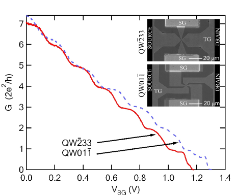
To answer these questions, we have studied a device consisting of two orthogonal 1D hole wires on a single Hall bar oriented along the high-mobility direction of an undoped (311)A AlGaAs/GaAs heterojunction. Electron micrographs of the two 400nm long wires, one aligned along and the other along , are shown in Fig. 1(inset), referred to hereafter as QW and QW. All measurements were performed with a top-gate voltage V corresponding to a hole density of cm-2. The width of the wire and its conductance can be gradually reduced by applying a positive voltage to the two side-gates (SG), as shown in Fig. 1 , until the wire is ‘pinched off’ at V. In each case, we observe the classic ‘staircase’ of quantized conductance plateaus at , where is the number of occupied 1D sub-bands, indicating ballistic transport through the wire vanWeesPRL88 ; KlochanAPL06 . Moving from left to right in Fig. 1 corresponds to strengthening the 1D confinement, taking the device from being quasi-2D (large and large ) to quasi-1D (small and small ). The similar pinch-off voltages for the two wires indicate that they have similar dimensions.
We study the spin properties of the 1D holes by measuring the Zeeman spin-splitting for different orientations of the wire and magnetic field with respect to the crystallographic axes. To obtain the -factor for the various 1D sub-bands , we use a technique that compares the 1D sub-band splitting due to an applied d.c. source-drain bias GlazmanEPL89 (see Fig. 2) and in-plane magnetic field PatelPRB91 (see Fig. 3). These two sets of measurements are repeated in two cool-downs (to rotate the sample) for the four different combinations of wire and magnetic field orientation with respect to the crystal axes.
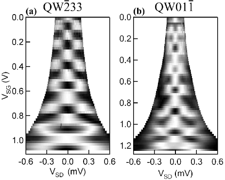
We first discuss the source-drain bias measurements shown in Fig. 2. We take the derivative of the conductance, (the transconductance), and plot it as a greyscale against and the voltage drop across the wire. The black regions correspond to high transconductance (the risers between plateaus) and white regions correspond to low transconductance (the plateaus themselves). As is increased the plateaus at multiples of evolve into plateaus at odd multiples of . The subband spacing is obtained from the source-drain bias at the centre of these odd-index plateaus The subband spacings for QW vary from 365 V () to 140 V (). The subband spacings for QW are slightly smaller, ranging from 282 V to 98 V. We repeated the subband spacing measurements on the second cooldown, and obtained identical results to within 10 V, confirming the stability and reproducibility of measurements obtained from these devices KlochanAPL06 .
The effect of an in-plane magnetic field on the 1D subbands is shown in Fig. 3 for different orientations of the quantum wire and magnetic field. The transconductance is plotted as a greyscale versus and . Again the black regions mark the 1D subband edges. For most orientations measured, the applied field causes spin-splitting of the 1D subbands, as in Fig. 3(c): Initially as is increased the subband edges move apart, and the conductance plateaus occur at multiples of PatelPRB91 ; DanneauPRL06 . If is increased further, 1D subbands with different spin orientations can cross, as seen in the right-hand side of Fig. 3(c), and the conductance plateaus then occur at odd multiples of . We were unable to observe this crossing in all orientations as the ohmic contacts degrade rapidly at T.
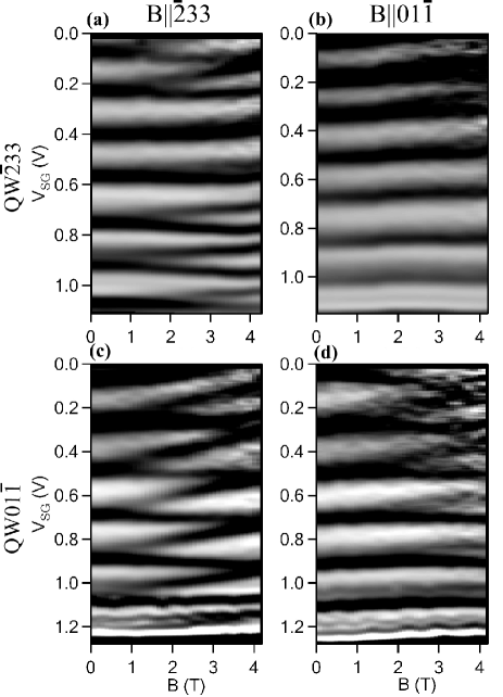
We now examine the spin-splitting for different orientations, starting with the wire aligned along . In Fig. 3(a) is aligned along the wire and spin-splitting is clearly observed (although the spin-splitting is not uniform for all 1D subbands, which we will discuss later). In contrast, for perpendicular to the wire, no splitting is observed up to the highest measured in any of the 1D subbands (Fig. 3(b)). These results are consistent with Ref. DanneauPRL06 , where 1D sub-band splitting was only visible for parallel to the wire. However for QW when is applied perpendicular to the the wire, strong spin-splitting is observed for all subbands, as shown in Fig. 3(c). For parallel to the wire, (Fig. 3(d)) spin-splitting is still observed, albeit weaker than in Fig. 3(c). Therefore, the anisotropy of the spin-splitting for QW is actually opposite to that of QW.
The anisotropic spin splitting in hole systems arises due to strong spin-orbit coupling, which means that these systems are best described by the total angular momentum . Strong spin-orbit coupling forces the quantization axis for the angular momentum to point perpendicular to the 2D plane, so the effective -factor takes different values depending on the relative orientation of and . For a 2D hole system grown on a high symmetry crystal plane, such as (100), this means that there is a spin-splitting if the magnetic field is applied perpendicular to the 2D plane, and no spin splitting if is applied in the 2D plane (). For lower symmetry growth directions, such as (311), cubic terms in the Hamiltonian due to crystallographic anisotropy result in a finite in-plane -factor WinklerBook03 with for and for . Confinement of the holes to a 1D wire causes the quantization axis for to lie along the wire in the 1D limit. In this case one expects that the -factor will be suppressed to lowest order if is not applied parallel to the wire.
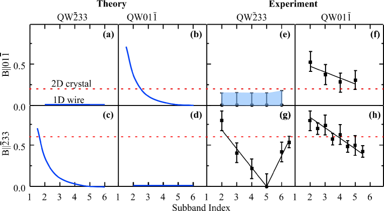
The expected behavior of is shown schematically in the first four panels of Fig. 4 as a function of the 1D subband index , for the different orientations of the wire and . The solid blue lines show the effect of the 1D confinement ignoring cubic crystal anisotropies. In the spherical approximation ZulickePSSC07 , the in-plane -factor is in all orientations in the 2D limit, and only becomes non-zero if is aligned along the wire (Figs. 4(b),(c)). For parallel to the wire, increases as the system becomes more 1D (lower ) and the quantisation axis aligns with the applied . The dashed red lines show the theoretical -factor in the 2D limit (large ) taking cubic crystal anisotropies into account. In our experiments we thus expect the -factor to show anisotropies due to a combination of the underlying properties of the (311) crystal and the 1D confining potential.
The stability of our devices and the high quality of the data allow us to compare our experimental data with these theoretical expectations by using the results in Figs. 2 and 3 to calculate for the four combinations of wire and field orientation, as shown in Figs. 4(e-h). The values of are obtained in two different ways DanneauPRL06 : For integer , we combine the subband splitting rate due to an applied d.c. bias, from Fig. 2, to the splitting rate due to an applied field, from Fig. 3, to obtain . The values obtained are plotted as solid symbols, with error bars marking the uncertainty in measured . The average -factor for two adjacent subbands can also be calculated using the 1D subband spacing and the field at which two subband edges of different spin orientations cross, giving where and are the d.c. bias and at the subband crossing. Data obtained in this way are plotted at half-integer values of . Finally, if the spin splitting is small it is difficult to extract . In such cases, we can only obtain an upper bound, indicated by the shaded region in Fig. 4(e).
The data in Fig. 4 indicate a complex dependence on wire and field orientation: We begin by considering for QW (Fig. 4(e)). In the 2D (large ) limit, the quantization axis points perpendicular to , and , as indicated by the dashed red line. This is consistent with our measurements, where the splitting is so small that we can only determine an upper bound for . In the 1D (small ) limit, the quantization axis is perpendicular to , strongly suppressing the Zeeman splitting, again giving very small -factors. Considering the wire aligned along with (Fig. 4(f)). At large , takes its expected 2D value of . Decreasing rotates the quantization axis from out-of-plane to along the axis of the wire, giving a corresponding enhancement of the spin splitting and an increase in . Note that this is not due to exchange enhancement, which is strongly suppressed for WinklerPRB05 .
For the remaining two cases, where lies along , the physics is more complex. For 2D holes in (311) heterostructures, the Zeeman term for the topmost heavy-hole subband contains three terms: , and , where the , and axes are the crystallographic directions , and , and are the relevant Pauli spin matrices (see Eqn. 7.13 of Ref. WinklerBook03 for details). The third term gives an anomalous out-of-plane spin polarization in response to along (which does not occur for ) WinklerPRB05 . It is this third term that causes the in-plane -factor anisotropy for (311) 2D hole systems, such that for is three times for , as indicated by the red dashed lines in Fig. 4 WinklerPRL00 . The anomalous spin polarization for also explains the difference in the -factor anisotropies between the two wires. For QW with (Fig. 4(h)), to first order we expect that since the quantization axis points out-of-plane in the 2D limit, should be suppressed (as in Fig. 4(f)). However, the term results in an out-of-plane spin polarization that enhances the Zeeman splitting so that . This is consistent with the measured data at large . We note a gradual increase in with decreasing in this orientation, which cannot be due to the 1D confinement because the quantization axis is perpendicular to the wire axis. The increased may be due to an exchange enhancement as the wire becomes more 1D – similar behavior is observed in 1D electron systems PatelPRB91N2 . Such an exchange enhancement can only happen for (311) holes for if the wire is perpendicular to WinklerPRB05 .
Finally, we come to QW and (Fig. 4(g)) which is the most complex and interesting case. The data clearly show a striking and unexpected non-monotonic behavior, with large for large and small , with dropping sharply for intermediate (confirmed with measurements of a second sample). The large and small limits are relatively straightforward to interpret. For large , the spin splitting is enhanced and due to the term caused by crystallographic anisotropy, as in Fig. 4(h). For small , the spin-splitting is also enhanced, but this time the 1D confinement tries to point the quantization axis along the wire and parallel to , in the same way as in Fig. 4(f). The complication comes at intermediate , because unlike in Fig. 4(f), where gradually increases as is reduced, in Fig. 4(g) it instead drops sharply almost to zero and then rises sharply with decreasing . This suggests that the transition between the initial 2D state and the final 1D state is made via an intermediate state with near-zero spin polarization (). One possibility is that this non-monotonic behavior is due to competition between the crystal anisotropy at large and the 1D confinement at small . Another possibility is that it may be due to orbital effects, since the shape of the wavefunction is affected both by the 1D confinement and the field applied along the wire. These results highlight the rich nature of spin-orbit coupling in 1D hole systems, and it would be extremely interesting to perform detailed calculations of the hole band-structure beyond the spherical approximation to shed further light on the anisotropic spin splitting in hole quantum wires ZulickePSSC07 .
Note: During completion of this paper related experimental work on hole quantum point contacts has appeared RokhinsonPRL2008 . In that work ’anomalous’ non-quantized plateaus were observed when both the quantum wire and were aligned along , in contrast to both this study and previous work on extremely high quality 1D holes where clean conductance plateaus are seen DanneauPRL06 . In addition Ref. RokhinsonPRL2008, finds the opposite behaviour of for quantum wires than reported here: A maximum in was found when is aligned along the wire, in contrast to the clear and unexpected minimum in shown in Fig. 4(g), where drops close to zero ().
This work was funded by Australian Research Council (ARC). O.K. and L.H.H. acknowledge support from UNSW and the CSIRO. A.R.H acknowledges an ARC Professorial Fellowship. We thank U. Zülicke and I.S. Terekhov for many helpful discussions and J. Cochrane for technical support.
References
- (1) S. A. Wolf, D. D. Awschalom, R. A. Burhman, J. M. Daughton, S. von Molnár, M. L. Roukes, A. Y. Chtchelkanova, & D. M. S. A. Treger, Science 294, 1488-1495 (2001).
- (2) G. Dresselhaus, Phys. Rev. 100, 580-586 (1955).
- (3) Yu. A. Bychkov & E.I. Rashba, JETP Lett. 39, 78 (1984).
- (4) S. Datta & B. Das, Appl. Phys. Lett. 56, 665-667 (1990).
- (5) L. Meier, G. Salis, I. Shorubalko, E. Gini, S. Schön, & K. Ensslin, Nature Physics 3, 650 (2007).
- (6) M. Y. Simmons, A. R. Hamilton, S. J. Stevens, D. A. Ritchie, M. Pepper & A. Kurobe, Appl. Phys. Lett. 70, 2750 (1997).
- (7) R. Winkler, Spin-orbit coupling effects in two-dimensional electron and hole systems (Springer Tracts in Modern Physics, Vol. 191, Springer, Berlin, 2003).
- (8) R. Winkler, S.J. Papadakis, E.P. de Poortere & M. Shayegan, Phys. Rev. Lett. 85, 4574 (2000).
- (9) S.J. Papadakis, E.P. de Poortere, M. Shayegan & R. Winkler, Phys. Rev. Lett. 84, 5592 (2000).
- (10) R. Danneau, O. Klochan, W. R. Clarke, L. H. Ho, A. P. Micolich, M. Y. Simmons, A. R. Hamilton, M. Pepper, D. A. Ritchie, & U. Zülicke, Phys. Rev. Lett. 97, 026403 (2006).
- (11) B.J. van Wees, H. van Houten, C. W. J. Beenakker, J. G. Williamson, L. P. Kouwenhoven, D. van der Marel, & C. T. Foxon, Phys. Rev. Lett. 60, 848 (1988).
- (12) O. Klochan, W. R. Clarke, R. Danneau, A. P. Micolich, L. H. Ho, A. R. Hamilton, K. Muraki, & Y. Hirayama, Appl. Phys. Lett. 89, 092105 (2006).
- (13) L. I. Glazman & A. V. Khaetskii, Europhys. Lett. 8, 263 (1989).
- (14) N. K. Patel, J. T. Nicholls, L. Martin-Moreno, M. Pepper, J. E. F. Frost, D. A. Ritchie, & G. A. C. Jones, Phys. Rev. B 44, 13549 (1991).
- (15) U. Zülicke, Phys. Stat. Sol C 3, 4354 (2007).
- (16) R. Winkler, E. Tutuc, S. J. Papadakis, S. Melinte, M. Shayegan, D. Wasserman, & S. A. Lyon, Phys. Rev. B 72, 195321 (2005).
- (17) N. K. Patel, J. T. Nicholls, L. Martin-Moreno, M. Pepper, J. E. F. Frost, D. A. Ritchie, & G. A. C. Jones, Phys. Rev. B 44, 10973 (1991).
- (18) S. P. Koduvayur, L. P. Rokhinson, D. C. Tsui, L. N. Pfeiffer, & K. W. West, Phys. Rev. Lett. 100, 126401 (2008).