Suspended single-electron transistors: fabrication and measurement
Abstract
We have fabricated aluminum single-electron transistors in which the island is not in contact with the substrate. This new type of device, which can be called suspended single-electron transistor (SUSET), displayed well-defined I-V and dI/dV-V features typical for high-quality standard SET’s.
The single-electron transistor (SET), a device proposed by Averin and Likharev in 1986 and first built by Fulton and Dolan in the next year averinlikharev , consists of a small metalic island connected to two leads (electrodes) by two tunnel junctions. The device is controlled through the voltage applied on a gate electrode capacitively coupled to the island.
The SET was proposed for a variety of applications, including counting electrons directly for a capacitance standard electrometer , direct measurements of single electron tunneling and co-tunneling, Bloch oscillations blochoscillations , and microwave photon detection sawphoton . There has been a lot of interest recently in the use of this device or relatively similar ones as quantum bits for a solid-state quantum computer squbits or as read-out systems for quantum circuits readouts . Finally, multiple-island devices such as Cooper pair pumps and single-electron turnstiles could find applications as metrological standards for current currentstandard or for measuring decoherence times in nanoscale superconducting systems jukka .
The Hamiltonian of an SET contains typically two parts: a tunneling Hamiltonian and a charge Hamiltonian. The first one can be either single-electron tunneling, if the SET is operated in the normal regime, or Josephson tunneling, in the case of a superconducting SET (Cooper-pair transistor). The charge Hamiltonian is given by the total energy associated with the electrostatic energy of the island plus the work done by sources to move the charge around the circuit. This energy contains also a phenomenological quantity usually called ”offset charge”, which brings an extra contribution to the energy even at zero voltages applied. This quantity takes different values for each device and cooldown and it fluctuates in time with an 1/f spectral density.
This effect limitates dramatically the usefulness of the device in many applications, for example it is the main constraining factor for the sensitivity of low-frequency SET electrometers (currently of the order of e/ lowfelectrometry ); the r.f.-SET improves this figure by paying the price of going up to higher frequencies, thus making the device more difficult to operate.
It is believed quantumamplifier that this phenomenon is caused by the trapped charge fluctuators in the oxide junction and the substrate; further careful investigations have led to the conclusion that the noise coming from the substrate dominates 1/f .
One idea to overcome these problems would be to try diferent substrates than the usual SiO2; indeed, the existing noise measurements in SET’s seem to suggest that there is a correlation between the type of substrate used and the minimum sensitivity achieved. This paper proposes a more radical approach to this issue: to eliminate the substrate itself. We demonstrate that it is indeed possible to fabricate working high-quality devices Al superconducting SET’s in which the island is not in contact with the substrate.
Although related free-standing structures have been fabricated before, most notably with semiconducting and metallic nanowires and carbon nanotubes suspended , active devices such as superconducting transitors have been available only on membranes or other types of specially designed supports. Besides immediate applications for present mesoscopic electrical circuits requiring low levels of substrate noise, one can speculate that these devices are relevant for building future hybrid solid state - atom (ion) systems which were recently proposed in the context of quantum computing zoller .

The suspended Al SET was fabricated using conventional two-angle evaporation on a nitridized Si wafer of 300 nm thickness followed by reactive ion etching. A double layer resist of PMMA-P(MMA-MAA) was spinned on the top of the SiN2 substrate and baked at 160∘C for 45 min (the bottom layer) and 60 min (the upper one). The resulting thicknesses of the PMMA and P(MMA-MAA) were approximately 250 nm and 350 nm, respectively. The mask was drawn using a scanning electron microscope (JEOL, JSM 840A) with acceleration voltage of 20 kV. The minimum width of the pattern in the island region was 50 nm; after the whole process, the thickness of the metalic wires increased to 100 nm. Then the resists were developed in a mixed solution (1:2) of methyl-iso-butylketon (MIBK) alcohol with isopropanol for about 30 s (the upper layer of PMMA) followed immediately by rinsing in isopropylic alcohol, and then in a mixture (1:2) of methyl glycol and methanol for roughly 8 s (the lower layer of P(MMA-MAA)). The chip was further cleaned in a reactive ion etcher (AXIC BENCHMARK) at 30 mTorr pressure with 50 sccm flow of O2 and 48 W RF-power for 30 s, a process that removes the resist leftovers from the SiN2 surfaces. The aluminum was evaporated in an UHV chamber at pressure of 2–4 mbar with an evaporation rate of 0.5 nm/s for both the island and the electrodes. The film, with a thickness of 40 nm, was then oxidized in a steady flow of O2, at a pressure of 20 mbar for three minutes. The junctions were formed by depositing another layer of 60 nm Al at a different angle. In the sample presented here, the 40 nm and 60 nm correspond to the island and the leads, respectively. The process was completed by lift-off, with the sample being slowly heated in acetone up to the boiling point (56C).
Finally the SET was put into a RIE (AXIC BENCHMARK) and etched in a two step process. The power was 10% (60 Watts), and the flow of O2 and CF4 was 10 % (5 sccm) and 50% (10.5 sccm) respectively. The first step was anisotropic etch at a pressure of 40 mTorr for 3 minutes (ion bombardment to break the surface of the nitride). The second step (isotropic etch) was at a pressure of 70 mTorr for 7 minutes.
The resulting structure is shown in Fig. 1 and Fig. 2. The length of the island is about 1m, and the thickness is approximately 100 nm.

The SUSET was measured in an electrically shielded room using a Nanoway PDR-50 dilution refrigerator with the lines filtered with commercial -filters at 4.2 K and a combination of -filters and RC-filters at room temperature. The conductance was measured using a lock-in amplifier technique. The results are presented in Fig. 3. The sample presented here had a room-temperature resistance k.
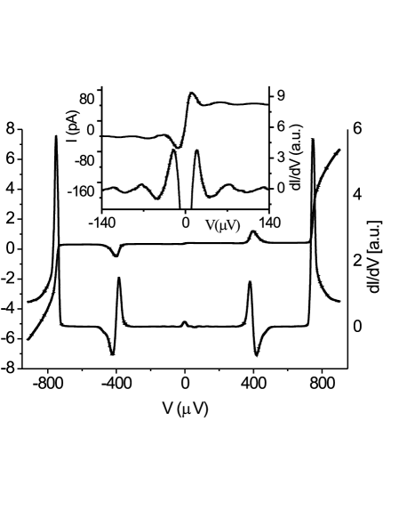

From the threshold voltage of the quasiparticle branch at 0.755 meV we can determine the gap of Al ( meV). The charging energy of the sample was derived from the Coulomb-blockade conductance measured at 4.2 K; we found a change in the zero-bias conductance peak , yielding a charging energy eV, where is the usual definition for the total capacitance of the island.
The critical Josephson current from Fig. 3 is approximately 70 pA; switching-current measurements, which are more precise, gave a value pA for this sample. This corresponds to a quite small Josephson energy eV. The Ambegaokar-Baratoff formula , where k is the quanta of resistance (von Klitzing constant), yields eV, significantly larger than the measured value. These are a well-known discrepancies for small-junction superconducting SET’s, caused by the sensitivity of the Josephson effect for small junctions to the external electromagnetic environment JJ . They occur when is larger or of the same order of magnitude as (therefore the phase of the island is not a good quantum number and the current has strong fluctuations), which is indeed the case for our sample.
In Fig. 3 the two symmetric peaks in the current are due to a combined Josephson and quasiparticle (JQP) tunneling in the junctions; this effect is predicted to happen at a bias voltage jqp . For our sample, this gives 0.391 meV 0.418 meV, in excellent agreement with the position of the peak in the experimental data. The JQP features are quite broad, as expected from the theory of this process for samples with small JQP-Tinkham .
Finally, a measurement at low bias voltages (inset of Fig. 3) reveals a finer structure of resonances in the current, corresponding to oscillations in the conductance. According to the theory of resonant tunneling of Cooper pairs resonances , the spacing between consecutive peaks peaks should be , i.e. 54 eV. Although the data were quite noisy, it was still possible to estimate the distance between peaks as being indeed 50-60 eV.
The SUSET is affected by temperature in the same way as conventional SET’s. Fig. 4 presents I-V measurements from 0.2 K to about 0.9 K, close to the critical temperature of Al. The low-temperature features get more rounded and they are displaced towards lower bias voltages, in agreement with the decrease of the gap of Al.
In conclusion, we have fabricated and measured a suspended SET. We did not observe any decrease in the quality of the device due to the extra etching process. Therefore, we believe that this new device can be useful in applications that require a precise control of the island charging as well as for investigations of the origin of the noise in single-electron transistors.
G. S. P. was supported by an EU Marie Curie Fellowship (HPMF-CT-2002-01893); A. P. H. was supported through the SQUBIT project (IST-1999-10673) of the European Union and the Academy of Finland Center of Excellence in Condensed Matter and Nuclear Physics at the University of Jyväskylä.
References
- (1) D. V. Averin and K. K. Likharev, J. Low Temp. Phys. 62, 345 (1986); T. A. Fulton and G. J. Dolan, Phys. Rev. Lett. 59, 109 (1987).
- (2) R. J. Schoelkopf, P. Wahlgren, A. A. Kozhevnikov, P. Delsing, and D. E. Prober, Science 280, 1238 (1998).
- (3) L. S. Kuzmin and D. B. Haviland, Phys. Scr. T 42, 171 (1992); J. Delahaye, J. Hassel, R. Lindell, M. Silanpää, M. Paalanen, H. Seppä, and P. Hakonen, Science 299, 1045 (2003).
- (4) J. M. Hergenrother, J. G. Lu, M. T. Tuominen, D. C. Ralph, and M. Tinkham, Phys. Rev. B 51, 9407 (1995); S. Komiyama, O. Astafiev, V. Antonov, T. Kutsuwa, and H. A. Hirai, Nature 403, 405 (2000).
- (5) Y. Nakamura, Y. A. Pashkin, and J. S. Tsai, Nature, 398, 786 (1999); J. E. Mooij, T. P. Orlando, L. Levitov, L. Tian, C. H. van der Val, and S. Lloyd, Science 285, 1036 (1999); J. R. Friedman, V. Patel, W. Chen, S. K. Tolpygo, and J. E. Lukens, Nature 406, 43 (2000); D. Vion, A. Aassime, A. Cottet, P. Joyez, H. Pothier, C. Urbina, D. Esteve, and M. H. Devoret, Science 296, 886 (2002); I. Chiorescu, Y. Nakamura, C. J. P. M. Harmans, and J. E. Mooij, Science 299, 1869 (2003); Yu. A. Paskin, T. Yamamoto, O. Astafiev, Y. Nakamura, D. V. Averin, and J. S. Tsai, Nature 421, 823 (2003).
- (6) Y. Makhlin, G. Schn, and A. Shnirman, Nature 386, 305 (1999); Yu. Makhlin, G. Schn, and A. Shnirman, Rev. Mod. Phys. 73, 357 (2001).
- (7) K. K. Likharev and A. B. Zorin, J. Low Temp. Phys., 59, 347 (1985); J. P. Pekola, J. J. Toppari, M. Aunola, M. T. Savolainen, and D. V. Averin, Phys. Rev. B 60, R9931 (1999).
- (8) J. P. Pekola and J. J. Toppari, Phys. Rev. B 64, 172509 (2001); R. Fazio, F. W. J. Hekking, and J. P. Pekola, Phys. Rev. B 68, 054510 (2003).
- (9) M. Tinkham, Introduction to Superconductivity, 2nd ed. (McGraw-Hill Inc., New York, 1996); M. T. Tuominen, J. M. Hergenrother, T. S. Tighe, and M. Tinkham, Phys. Rev. Lett. 69, 1997 (1992).
- (10) E. N. Visscher, S. M. Verbrugh, J. Lindeman, P. Hadley, and J. E. Mooij, Appl. Phys. Lett. 66, 305 (1995); V. A. Krupenin, D. E. Presnov, M. N. Savvateev, H. Scherer, A. B. Zorin, and J. Niemeyer, J. Appl. Phys. 84, 3212 (1998).
- (11) M. H. Devoret, R. J. Schoelkopf, Nature 406, 1039 (2000).
- (12) A. B. Zorin, F.-J. Ahlers, J. Niemeyer, T. Weiman, H. Wolf, V. A. Krupenin, and S. V. Lotkhov, Phys. Rev. B 53, 13682 (1996); N. M. Zimmerman, J. L. Cobb, and A. F. Clark, Phys. Rev. B 56, 7675 (1997).
- (13) D. G. Hasko, A. Potts, J. R. Cleaver, C. G. Smith, and H. Ahmed, J. Vac. Sci. Technol. B 6, 1849 (1988); C. G. Smith, H. Ahmed, and M. N. Wybourne, J. Vac. Sci. Technol. B 5, 314 (1987); L. Roschier, R. Tarkiainen, M. Ahlskog, M. Paalanen, and P. Hakonen, Appl. Phys. Lett. 78, 3295 (2001).
- (14) L. Tian, P. Rabl, R. Blatt, and P. Zoller, Phys. Rev. Lett., 92, 247902 (2004); A. S. Sørensen, Phys. Rev. Lett. 91, 063601 (2004).
- (15) P. Joyez, D. Vion, M. Götz, M. H. Devoret, and D. Esteve, Journal of Superconductivity, 12, 757 (1999); A. Steinbach, P. Joyez, A. Cotet, D. Esteve, M. H. Devoret, M. E. Huber, and J. M. Martinis, Phys. Rev. Lett. 87, 137003 (2001).
- (16) T. A. Fulton, P. L. Gammel, D. J. Bishop, L. N. Dunkleberger, and G. J. Dolan, Phys. Rev. Lett. 63, 1307 (1989); Y. Nakamura, C. D. Chen, and J. S. Tsai, Phys. Rev. B 53, 8234 (1996).
- (17) S. L. Pohlen, R. J. Fitzgerald, and M. Tinkham, Physica B 284-288, 1812 (2000).
- (18) A. Maassen van den Brink, A. A. Odintsov, P. A. Bobbert, and G. Schn, Z. Phys. B 85, 459 (1991); D. B. Haviland, Y. Harada, P. Delsing, C. D. Chen, and T. Claeson, Phys. Rev. Lett. 73, 1541 (1993); Y. Harada, D. B. Haviland, P. Delsing, C. D. Chen, and T. Claesson, Appl. Phys. Lett. 65, 636 (1994).