Quantum scaling in nano-transistors
Abstract
In our previous papers on ballistic quantum transport in nano-transistors [J. Appl. Phys. 98, 84308 (2005)] it was demonstrated that under certain conditions it is possible to reduce the three-dimensional transport problem to an effectively one-dimensional one. We show that such an effectively one-dimensional description can be cast in a scale-invariant form. We obtain dimensionless variables for the characteristic channel length and width of the transistor which determine the scale-invariant output characteristic. For , in the strong barrier regime, the output characteristics are similar to that of a conventional MOSFET assuming an ideal form for . In the weak barrier regime, , strong source-drain currents lead to i-v characteristics that differ qualitatively from that of a conventional transistor. Comparing with experimental data we find qualitative agreement.
pacs:
73.23.A,03.65.Xp,73.63.-bRecently, a number of extremely small nano-transistors with physical gate lengths of fifteen nanometers or less have been fabricatedWakabayashi et al. (2003); Doyle et al. (2002); Yu et al. (2001). A rather simple but particularly illuminating approach to describe the electron dynamics in such small structures is to assume ballistic quantum transport (for a recent review see Ref. [Lundstrom and Guo, 2006]). It is found for a long enough electron channel that the output characteristic is similar to that of a conventional transistor. However, in this quantum ballistic transistor (QBT) regime source-drain tunneling currents cause residual slopes in the ON-state and the development of only a quasi-OFF-state. In Refs. [Nemnes et al., 2004, 2005] it was shown that separating the ON-state of classically allowed transport and the quasi OFF-state of tunneling transport there is a threshold characteristic (TH) which exhibits a close-to-linear dependence of the current on the drain voltage. Above the TH, in the ON-state, the I-V curves are characterized by a negative bending and below the TH by a positive bending. In Refs. [Nemnes et al., 2004, 2005] it was furthermore demonstrated that for a narrow electron channel the complete three-dimensional quantum problem can be approximated by an effectively one-dimensional one (Fig. 1).
In the present paper we recast our effectively one-dimensional description of quantum transport in a nano-transistor in a scale-invariant form. The scaled output characteristics of a transistor are governed by its dimensionless characteristic length and the width , which are given by its physical length and width in units of the scaling length . Here is the Fermi energy in the source contact and is the effective mass in the electron channel in transport direction. The characteristic length permits a classification of source-drain barriers in terms of their strength. In the strong barrier regime, , typical output characteristics in the QBT regime occur. As , ideal output characteristics (IOC) are assumed with a vanishing residual slope in the ON-state and a clear OFF-state exhibiting negligible leakage currents. In the weak barrier regime, , strong source-drain currents lead to I-V characteristics which differ strongly from that of a conventional transistor. In the limit of large we relate our scaling theory to the experiments and find qualitative agreement.
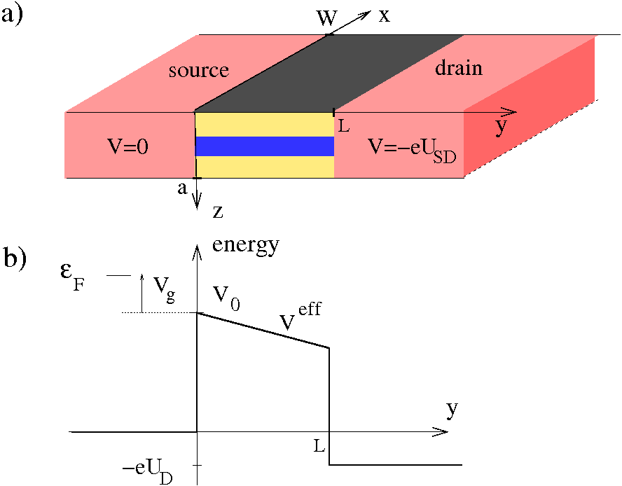
In Fig. 1 our effective potential is illustrated. Though simple, it allows us to define the essential parameters: because of good screening it is constant in the source contact with and in the drain contact with , where is the applied drain voltage. The source-drain barrier is taken as a constant potential offset for . In the latter interval there is an additional contribution due to the applied drain voltage which is assumed to fall off linearly so that . Such a piecewise linear potentialUeno et al. (2002) or more complex potentials with the same qualitative behaviorLundstrom and Guo (2006) have been used in the literature. We calculate the drain current through
| (1) |
with the normalized drain current , , and , and . The current transmission results from the transmission coefficient of a source-incident scattering function in a one-dimensional scattering problem associated with the effective Schrödinger equation
| (2) |
Here we have , , , , , and . The three-dimensional geometry of the transistor determines the choice of the supply function . For a narrow transistor (small ) it was shown in Ref. [Nemnes et al., 2005] that at it is given by . In a straightforward way one can generalize this result to a wide transistor yielding , with the normalized transistor width Wulf and Kucera .
To consider an I-V chart we represent the gate potential by the parameter , which is the deviation of the Fermi energy in the source contact from the maximum of the source-drain barrier (see Fig. 1 (b)). Normalized to one has , allowing us to eliminate in Eq. (1). Furthermore, we define new variables and . These are normalized to , which is independent of the gate voltage. To cast and in terms of and in Eq. (1) one exploits the identities and . Furthermore, the parameter is replaced by , where we introduce the dimensionless characteristic length of the transistor as with the scaling length
| (3) |
Likewise , where we introduce the characteristic width of the transistor as .
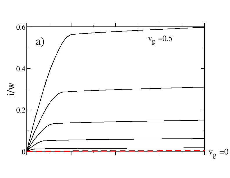
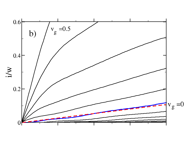
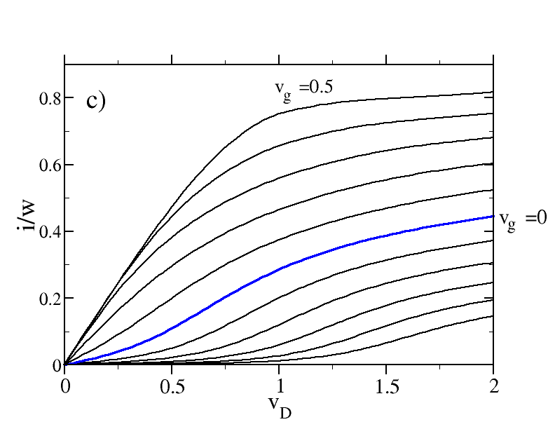
The calculated traces in Figs. 2 (a) and (b) exemplify the QBT regime at . For positive , i.e. in the ON-state, an initial linear dependence of the drain current for small drain voltages turns into a quasi-saturation regime for larger drain voltages. The turnover between linear and quasi-saturation regime becomes more and more abrupt, which is seen in the experimental transistors in Fig. 3 (a) and (b) as well. The essentially linear THs at allow us to define a threshold conductivity through . Upon analysis of the numerical data it can be seen that in the range of interest one can approximate with an error of less than 10 percent . This weak power law decrease indicates that the IOC are assumed slowly with growing and that there is no critical characteristic length to define a hypothetical ‘ideal transistor regime´. As shown in Fig. 2 (c) in the weak barrier limit, , I-V traces differ strongly from that of a conventional field effect transistor because of strong source-drain tunneling and no TH is observed.
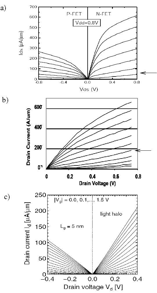
For a rough estimate of the characteristic lengths in the experimental nano-transistors in Fig. (3) we approximate by the well-known expression for a three-dimensional non-interacting electron gas. Assuming a high level of source-doping of yields . Inserting in Eq. (3) furthermore the silicon light mass, , one obtains . The experimental channel lengths of to then correspond to characteristic lengths of five, ten, and fifteen. As expected we find for a close-to linear TH with an experimental threshold slope for and for . Writing one obtains for a theoretical value for of and for a theoretical value of . While the decrease in the threshold conductivity results theoretically and experimentally, there is a considerable quantitative discrepancy which is to be expected because in our model essential effects like heating of the transistor and microscopic Coulomb interaction are not included. Consistent with Fig. 2 (c) the I-V characteristics of the experimental transistor with 5nm gate length in Fig. 3 (c) seem to deviate considerably from the output characteristic of conventional transistor. However, for a characterization of the breakdown of the QBT-regime for weak barriers further research is needed. Finally, we note that in the range of the experimental the barrier strength could be increased using metal contacts like in a Schottky barrier transistorKnoch et al. (2007). Here larger are possible which according to Eq. (3) lead to smaller and larger .
In summary, we present a scaling theory for quantum transport in nano-transistors. The scaled i-v characteristics depend on the dimensionless characteristic length of the transistor channel which allows for a classification of a given source-drain barrier in terms of its strength. In the strong barrier regime, , the output characteristics are similar to that of a conventional MOSFET assuming an ideal form for . In the weak barrier regime strong source-drain currents occur and the i-v characteristics differ strongly from that of a conventional transistor.
We thank J. Emtage for valuable discussions.
References
- Wakabayashi et al. (2003) H. Wakabayashi, S. Yamagami, N. Ikezawa, A. Ogura, M. Narihiro, K. Arai, Y. Ochiai, K. Takeuchi, T. Yamamoto, and T. Mogami, IEDM Tech. Dig. p. 989 (2003).
- Doyle et al. (2002) B. Doyle, R. Arghavani, D. Barlage, S. Datta, M. Doczy, J. Kavalieros, A. Murty, and R. Chau, Intel Technology Journal 6, 42 (2002).
- Yu et al. (2001) B. Yu, H. Wang, A. Joshi, Q. Xiang, E. Ibok, and M.-R. Lin, IEDM Tech. Dig. p. 937 (2001).
- Lundstrom and Guo (2006) M. Lundstrom and J. Guo, Nanoscale Transistors (Springer, Berlin, 2006).
- Nemnes et al. (2004) G. A. Nemnes, U. Wulf, and P. N. Racec, J. Appl. Phys. 96, 596 (2004).
- Nemnes et al. (2005) G. A. Nemnes, U. Wulf, and P. N. Racec, J. Appl. Phys. 98, 84308 (2005).
- Ueno et al. (2002) H. Ueno, M. Tanaka, K. Morikawa, T. Takayashi, and M. Miura-Mattausch, J. Appl. Phys. 91, 5360 (2002).
- (8) U. Wulf and J. Kucera, in preparation.
- Knoch et al. (2007) J. Knoch, M. Zhang, J. Appenzeller, and S. Mantl, Appl. Phys. A 87, 351 (2007).