Bound-state third-order optical nonlinearities of embedded germanium nanocrystals
Abstract
Embedded germanium nanocrystals (NCs) in a silica host matrix are theoretically analyzed to identify their third-order bound-state nonlinearities. A rigorous atomistic pseudopotential approach is used for determining the electronic structure and the nonlinear optical susceptibilities. This study characterizing the two-photon absorption, nonlinear refractive index, and optical switching parameters reveals the full wavelength dependence from static up to the ultraviolet spectrum and the size dependence up to a diameter of 3.5 nm. Similar to Si NCs, the intensity-dependent refractive index increases with decreasing NC diameter. On the other hand, Ge NCs possess about an order of magnitude smaller nonlinear susceptibility compared to Si NCs of the same size. It is observed that the two-photon absorption threshold extends beyond the half band-gap value. This enables nonlinear refractive index tunability over a much wider wavelength range free from two-photon absorption.
pacs:
42.65.-k, 42.65.Ky, 78.67.BfI Introduction
Semiconductor nanocrystals (NCs) benefit from the accumulated knowledge in semiconductor physics and the maturity of the semiconductor industry as well as the new opportunities provided by the nanoscience, hence they offer unique optical properties.gaponenko05 In particular, Si and Ge NCs attract an increasing attention because of their low-cost and microelectronic-compatible photonic applications ranging from light emitting diodes and lasers to solar cells and other photonic devices.pavesi04 ; reed Even though Si and Ge are both Group IV elements, there are a number of notable differences between them such as the band edge effective mass of the carriers are smaller for Ge, whereas the dielectric constant is larger which results in bulk exciton radius about five times larger for Ge compared to Si.yu-cardona As a result, the confinement effects will be felt starting from larger sizes. Moreover, Ge is a weakly indirect band-gap semiconductor with the direct to indirect band-gap ratio being 1.2, in contrast to 2.9 in Si. Furthermore, the narrower band-gap of the bulk as well as the NC Ge can be preferred in certain applications to harvest the near infrared part of the spectrum.healy92 Finally, the proximity of direct-gap optical transitions in bulk Ge to the fiber optic communication wavelength of 1.5 m range is particularly important. This has recently stimulated extensive interest; notably tensile-strained Ge photodetectors on Si platform has been demonstrated liu05 and a tensile-strained Ge-based laser is proposed.liu07 If the latter can also be experimentally demonstrated, this will mark the dawn of the germanium photonics era.
For all-optical switching and sensor protection applicationsboyd03 as well as in the absorption of the subband-gap light for the possible solar cell applications,thurpke the nonlinear refractive index coefficient also known as the optical Kerr index, , and two-photon absorption coefficient, , are the two crucial third-order optical nonlinearities which play an important role. Recent experiments show that Ge NCs have enhanced third-order optical nonlinearities.dowd99 ; jie00 ; li01 ; wan03 ; razzari06 ; gerung06 However, differences in the sample preparation methods, the choice of the matrix, the excitation laser wavelength and the size distribution of the NCs contribute to the wide variance within these results as shown in Table I. A number of these investigations have observed two characteristic temporal nonlinear response contributions, distinguished as fast and slow, but there is no quantitative agreement among themselves.dowd99 ; li01 ; razzari06 Regarding the origin of the nonlinear response, some of these reports have stressed the role of the excited-state contribution produced by the linear absorption,jie00 ; li01 ; razzari06 also the involvement of the trap/defect states was addressed.dowd99 ; razzari06 Undoubtedly, more experiments are needed to reach to a coherent understanding. On the other hand, to the best of our knowledge, there is no theoretical study identifying the wavelength and size dependences of and in Ge NCs. Therefore, a rigorous theoretical work may guide and inspire further experimental studies on the foregoing investigations. Moreover, it would help in assessing the potential role of Ge NCs, if any, in nonlinear device applications mentioned above.
In this paper, our aim is to present such a theoretical account concerning and in Ge NCs revealing their size scaling and wavelength dependence from static up to ultraviolet region together with a comparison with Si NCs. Furthermore, we deal with NCs embedded in a wide band-gap matrix representing silica which is the most common choice in the actual structures as can be observed in Table I. Since we do not consider any interface defects, strain and thermal effects or the compounding contribution of the excited carriers through linear absorption to the nonlinear processes, our results may serve as a benchmark of the ideal Ge NC bound-state ultrafast third-order nonlinearities. In Sec. II we describe the theoretical approach for the electronic structure and the expressions for nonlinear optical quantities. The results and discussions are provided in Sec. III followed by a brief conclusion.
| Reference | (nm) | (nm) | (cm2/GW) | (cm/GW) | Matrix | Preparation |
|---|---|---|---|---|---|---|
| Ref.dowd99, | 3 | 800 | 2.7-6.9 | silica | ion implantation | |
| Ref.jie00, | 61.8 | 532 | 2.6-8.2 | 190-760 | silica | cosputtering |
| Ref.li01, | 61.8 | 780 | 1.5-8 | 0.18-0.68 | silica | cosputtering |
| Ref.wan03, | 5.8, 6.4 | 532 | 95.4, 143 | alumina | E-beam coevaporation | |
| Ref.razzari06, | 800 | 1 | 0.04 | silica | PECVD | |
| Ref.gerung06, | 52 | 820 | 1190-1940 | solution | chemical synthesis |
II Theory
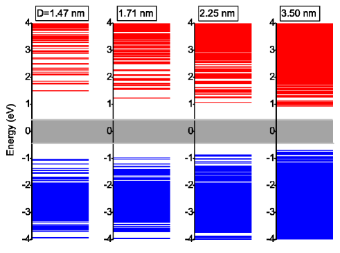
The electronic structure of nanoclusters are accurately obtained routinely by means of density functional theory-based ab initio techniques.martin-book However, a several nanometer-diameter NC system including the embedding host matrix contains thousands of atoms. This large number currently precludes the use of such ab initio pseudopotential plane wave techniques. An alternative route is based on the use of semi-empirical pseudopotential description of the atomic environmentchelikowsky in conjunction with the linear combination of Bloch bands as the expansion basis.ninno85 ; wang97 In the case of embedded Si and Ge NCs, this yields results in well agreement with experimental data for the interband, intraband optical absorptionbulutay07 and the Auger recombination and carrier multiplication.sevik08 All of these are governed by quantum processes taking place over several electronvolt energy range. As a matter of fact, this feature forms an essential support for applying the approach to the characterization of the third-order nonlinear susceptibilities up to a photon energy of 4 eV. We refer to our previous work for further details on the electronic structure.bulutay07 The corresponding electronic structure for embedded Ge NCs of different sizes are shown in Fig. 1. The evolution of the effective gap, towards the bulk value (as marked by the gray band) can be observed as the NC diameter increases which is the well-known quantum size effect.
In this work, the electromagnetic interaction Hamiltonian is taken as , in other words, the length gauge is used. The third-order optical nonlinearity expressions based on the length gauge have proved to be successful in atomic-like systemsboyd03 but not in bulk systems because the position operator introduces certain difficulties which can actually be overcome.aversa95 Nevertheless, for bulk systems the velocity gauge has been preferred which on the other hand possesses unphysical divergent terms at zero frequency (not present in the length gauge) that poses severe obstacles in evaluating the nonlinear optical expressions.sipe00 Hence, we have preferred the length gauge for the evaluation of the third-order optical expressions due to resemblance of the band structure of NCs to atomic-like systems (cf. Fig. 1). The susceptibility expression is obtained through perturbation solution of the density matrix equation of motion.boyd03 Throughout this work, we distinguish the quantities which refer to unity volume filling factor by an overbar, where is the volume filling factor of the NC in the matrix, and are the volumes of the NC and supercell, respectively. The final expression is given byboyd03
| (1) |
where the subscripts refer to Cartesian indices, , , are the input frequencies, is the matrix element of the position operator between the states and , is the difference between energies of these states, S is the symmetrization operator,boyd03 indicating that the following expression should be averaged over the all possible permutations of the pairs , , and , and finally where is the occupancy of the state . The is calculated for through where is the free electron mass, and is the momentum matrix element. Hence, after the solution of the electronic structure, the computational machinery is based on the matrix elements of the standard momentum operator, P, the calculation of which trivially reduces to simple summations.
The above susceptibility expression is evaluated without any approximation taking into account all transitions within the 7 eV range. This enables a converged spectrum up to the ultraviolet spectrum. In the case of relatively large NCs the number of states falling in this range becomes excessive making the computation quite demanding. For instance, for the 3 nm NC the number of valence and conduction states (without the spin degeneracy) become 3054 and 3314, respectively. As another technical detail, the perfect symmetry of the spherical NCs bulutay07 results in an energy spectrum with a large number of degenerate states. However, this causes numerical problems in the computation of the susceptibility expression given in Eq. (1). This high symmetry problem can be practically removed by introducing two widely separated vacancy sites deep inside the matrix. Their sole effect is to introduce a splitting of the degenerate states by less than 1 meV.
When solids are excited with light having a frequency below the band-gap at intensities high enough, third-order changes in the refractive index and the absorption are observed due to the virtual excitations of the bound charges. Accounting for these effects, the refractive index and the absorption become, respectively, , , where is the linear refractive index, is the linear absorption coefficient, and I is the intensity of the light. is proportional to , and is given bybahae90
| (2) |
where c is the speed of light. Similarly, is given bybahae90
| (3) |
where is the angular frequency of the light. Note that Eqs. (2) and (3) are valid only in the case of negligible absorption. The degenerate two-photon absorption cross section is given byboyd03
| (4) |
where is the inverse of the lifetime; the corresponding full width energy broadening of 100 meV is used throughout this work. The sum over the intermediate states, , requires all interband and intraband transitions. As we have mentioned previously we compute such expressions without any approximation by including all states that contribute to the chosen energy window. Finally, and are related to each other through .
Another important factor is the so-called local field effect (LFE) which arise in composite materials of different optical properties; the LFEs lead to a correction factor in the third-order nonlinear optical expressions given by,sipe02 where and are the dielectric functions of the host matrix and the NC, respectively. We fix the local field correction at its static value, since when the correction factor is a function of the wavelength it brings about unphysical negative absorption regions at high energies. Further discussions of our model are available in our previous work.yildirim08
III Results and Discussion
We have performed extensive computations on Ge NCs with six different diameters, namely, , 1.47, 1.71, 2.25, 3, and 3.5 nm. For , and 3.5 nm sizes which correspond to smallest and largest diameters, we have calculated the nonlinearities at certain important laser wavelengths. As for the rest, the nonlinearities are computed at all frequencies up to 4 eV. For generality, we quote the unity-filling-factor values denoted by an overbar which can trivially be converted to any specific realization, however, we should caution that the actual amount of Ge atoms forming the NCs is usually a small fraction of the overall excess Ge atoms most of which disperse in the matrix without aggregating into a significant NC. In accounting for the LFE the host matrix is assumed to be silica which is the most common choice (cf., Table I).
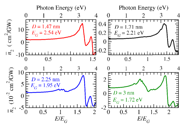
Under these conditions, is plotted in Fig. 2 as a function photon energy both in eV (upper abscissas) and in units of effective gap, (lower abscissas). As expected, below half (i.e., in the transparency region), there is a monotonous behavior and above this value the resonances take over. An intriguing observation is about the sign of . In general, bulk semiconductors change the sign of above their half values.bahae91 However, in Fig. 2 we observe that in Ge NCs this takes place at even beyond ; for the and 3 nm NCs, the emergence of a new resonance is seen to develop which can possibly reproduce this sign change at lower than values for the larger NCs. This negative sign of is known to be caused by both the two-photon absorption and the ac Stark effect.bahae91 In the size range considered in this work, we believe the former to be more dominant in the negative sign of . For nm NC, and below 1 eV, is of the order of cm2/GW. This value is much larger than the bulk value.bahae91 When compared to the available Ge NC measurements in Table I, this is in very good agreement with Jie et al.jie00 given the discrepancy in the NC size and the host matrix. On the other hand, other measurements are about three orders of magnitude lower for the same quantity.
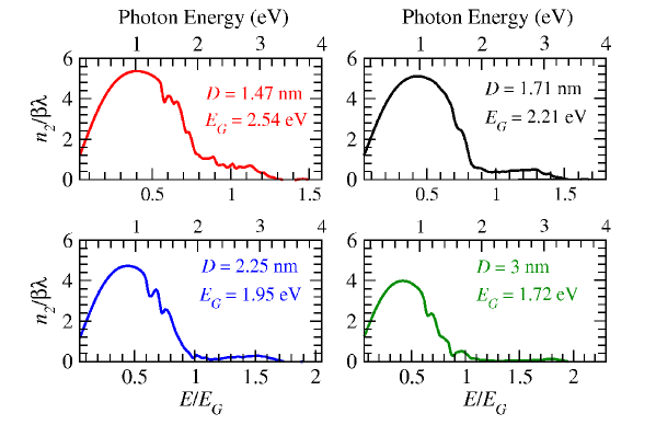
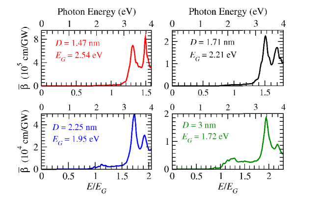
The situation is similar in the case of which is plotted against the photon energy in Fig. 3. An important observation is that the two-photon absorption onset lies further beyond the half band gap value which is possibly a manifestation of the indirect band gap nature of the core medium. We should note that is nonzero (albeit very small) down to static values due to band tailinglloyd which is represented as in our previous work on Si NCsyildirim08 through the Lorentzian energy broadening parameter, , of 100 meV at full width. For nm NC, has a value cm/GW around 2 eV. This value is very high compared to the corresponding bulk value.rauscher97 When typical volume filling fraction is taken into account, our values are again in order of magnitude agreement with Gerung et al.gerung06 and Jie et al.jie00 both of which are for somewhat larger NCs. It should be noted that there is an outstanding disagreement among the experimental data; for instance, the two most recent experimental data measured at very close photon energies differ by five orders of magnitude.razzari06 ; gerung06 This emerging picture about the large discrepancy on the and values calls for further experimental investigations, especially probing the ultrafast response.
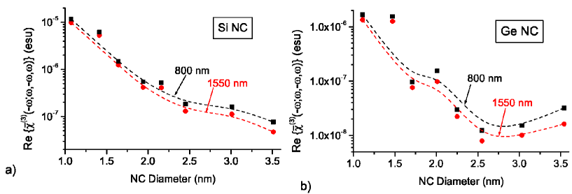
The comparison of the size-scaling trends of the real part of the third-order susceptibility for Si and Ge NCs are shown in Fig. 4. Two different wavelengths are used, 1550 nm and 800 nm both of which fall below the band gap, hence they do not experience any linear absorption. Again unity volume filling factor values are quoted. It can be observed that for both Si and Ge NCs, there is a common enhancement trend (dashed lines) as the size is reduced especially below 2.5 nm. The oscillations for certain diameters is common to both materials, however, they are more pronounced in the Ge NCs. This corroborates with the size scaling of the Auger and carrier multiplication lifetimes.sevik08 Another important finding is that third-order susceptibility of Si NCs are more than 20 times larger compared to Ge NCs of the same size embedded in the same host matrix.
For optical switching and modulation applications, one needs large tunability of the refractive index, such as through the optical Kerr effect without an appreciable change in the attenuation. Hence, as the figure of merit, is proposed.bahae91 In our previous work, we have observed that the Si NCs possess much superior figure of merit parameters compared to bulk Si.yildirim08 Fig. 5 shows that Ge NCs closely resemble the results of Si NCs.yildirim08 Both Si and Ge NCs benefit from the significant blue shift of the onset of the two-photon absorption from the half value, which enables the design of such switching or modulation elements over an extended wavelength range. A further indirect advantage of this could be the suppression of the optical loss introduced by two-photon absorption generated carriers at moderately high pump powers which was a major concern in silicon Raman amplifiers.liang
IV Conclusions
In summary, we have investigated the wavelength and size dependence of the third-order optical nonlinearities in Ge NCs, where our results can serve as a benchmark of the bound-state contribution reflecting the ultrafast response of an unstrained perfect sample with no size dispersion. Our computed values for and are in agreement with some of the existing experimental data which contain several orders of magnitude disagreement among themselves. We observe that below the band gap, there is a common enhancement trend of both the real and imaginary parts of the third-order susceptibility as the NC size is reduced. Another important finding is that third-order susceptibility of Ge NCs are about an order of magnitude smaller compared to Si NCs of the same size and embedded in the same dielectric environment. As in the case of Si NCs, the two-photon absorption threshold extends beyond the half band-gap value. This enables nonlinear refractive index tunability over a much wider wavelength range free from two-photon absorption. As a final remark, our investigation calls for further experimental work especially to probe the ultrafast third-order nonlinear response of Ge NCs.
Acknowledgements.
This work has been supported by the Turkish Scientific and Technical Council TÜBİTAK with the project number 106T048 and by the European FP6 Project SEMINANO with the contract number NMP4 CT2004 505285. The authors would like to thank Dr. Can Uğur Ayfer for the access to Bilkent University Computer Center facilities. H.Y. acknowledges TÜBİTAK-BİDEB for the financial support.References
- (1) S. V. Gaponenko, Optical Properties of Semiconductor Nanocrystals, (Cambridge University, 2005).
- (2) L. Pavesi and D. J. Lockwood, Silicon Photonics, (Springer, Berlin, 2004).
- (3) G. T. Reed and A. P. Knights, Silicon Photonics: An Introduction, (Wiley, Chichester, 2004).
- (4) P. Y. Yu and M. Cardona, Fundamentals of Semiconductors, (Springer, Berlin, 1996).
- (5) S. A. Healy and M. A. Green, Sol. Energy Mater. Sol. Cells 28, 273 (1992).
- (6) J. Liu, D. D. Cannon, K. Wada, Y. Ishikawa, S. Jongthammanurak, D. T. Danielson, J. Michel, and L. C. Kimerling, Appl. Phys. Lett. 87, 011110 (2005).
- (7) J. Liu, X. Sun, D. Pan, X. Wang, L. C. Kimerling, T. L. Koch and J. Michel, Opt. Express 15, 11272 (2007).
- (8) R. W. Boyd, Nonlinear Optics, (Academic Press, San Diego, CA, 2003).
- (9) T. Thurpke, M. A. Green, and P. Würfel, J. Appl. Phys. 92, 4117 (2002).
- (10) A. Dowd, R. G. Elliman, M. Samoc, and B. Luther-Davies, Appl. Phys. Lett. 74, 239 (1999).
- (11) Y. X. Jie, Y. N. Xiong, A. T. S. Wee, C. H. A. Huan, and W. Ji, Appl. Phys. Lett. 77, 3926 (2000).
- (12) H. P. Li, C. H. Kam, Y. L. Lam, Y. X. Jie, W. Ji, A. T. S. Wee, and C. H. A. Huan, Appl. Phys. B: Lasers Opt. 72, 611 (2001).
- (13) Q. Wan, C. L. Lin, N. L. Zhang, W. L. Liu, G. Yang, and T. H. Wang, Appl. Phys. Lett. 82, 3162 (2003).
- (14) L. Razzari, A. Gnoli, M. Righini, A. Dâna, and A. Aydinli, Appl. Phys. Lett. 88, 181901 (2006).
- (15) H. Gerung, Y. Zhao, L. Wang, R. K. Jain, T. J. Boyle, C. J. Brinker, and S. M. Han Appl. Phys. Lett. 89, 111107 (2006).
- (16) R. M. Martin, Electronic Structure, Cambridge University Press, Cambridge (2004).
- (17) M. L. Cohen and J. R. Chelikowsky, Electronic Structure and Optical Properties of Semiconductors, (Springer, Berlin, 1988).
- (18) D. Ninno, K. B. Wong, M. A. Gell, and M. Jaros, Phys. Rev. B 32, 2700 (1985).
- (19) L. W. Wang, A. Franceschetti, and A. Zunger, Phys. Rev. Lett. 78, 2819 (1997).
- (20) C. Bulutay, Phys. Rev. B 76, 205321 (2007).
- (21) C. Sevik and C. Bulutay, Phys. Rev. B 77, 125414 (2008).
- (22) C. Aversa and J. E. Sipe, Phys. Rev. B 52, 14636 (1995).
- (23) R. W. Boyd, Nonlinear Optics, p. 173 (Academic Press, San Diego, CA, 2003).
- (24) J. E. Sipe and A. I. Shkrebtii, Phys. Rev. B 61, 5337 (2000).
- (25) H. Yıldırım and C. Bulutay, Opt. Commun. 281, 4118 (2008).
- (26) P. Lloyd, J. Phys. C: Solid State Phys. 2, 1717 (1969).
- (27) M. Sheik-Bahae, A. A. Said, T. H. Wei, D. J. Hagan, and E. W. Van Styrland, IEEE J. Quantum Electron. 26, 760 (1990).
- (28) J. E. Sipe and R. W. Boyd, in Optical Properties of Nanostructured Random Media, Topics Appl. Phys., edited by V. M. Shalev (Springer, Berlin-Heidelberg, 2002), Vol. 82, pp. 1-19.
- (29) C. Rauscher and R. Laenen, J. Appl. Phys. 81, 2818 (1997).
- (30) M. Sheik-Bahae, D. C. Hutchings, D. J. Hagan, and E. W. Van Stryland, IEEE J. Quantum Electron. 27, 1296 (1991).
- (31) T. K. Liang and H. K. Tsang, Appl. Phys. Lett. 84, 2745 (2004).