Tight–binding description of the quasiparticle dispersion of graphite and few–layer graphene
Abstract
A universal set of third–nearest neighbour tight–binding (TB) parameters is presented for calculation of the quasiparticle (QP) dispersion of stacked graphene layers () with stacking sequence. The QP bands are strongly renormalized by electron–electron interactions which results in a 20% increase of the nearest neighbour in–plane and out–of–plane TB parameters when compared to band structure from density functional theory. With the new set of TB parameters we determine the Fermi surface and evaluate exciton energies, charge carrier plasmon frequencies and the conductivities which are relevant for recent angle–resolved photoemission, optical, electron energy loss and transport measurements. A comparision of these quantitities to experiments yields an excellent agreement. Furthermore we discuss the transition from few layer graphene to graphite and a semimetal to metal transition in a TB framework.
I Introduction
Recently mono– and few–layer graphene (FLG) in an (or Bernal) stacking is made with high crystallinity by the following three methods; epitaxial growth on SiC seyller06-sic , chemical vapour deposition on Ni(111) alex07-graphenenickel and by mechanical cleavage on novoselov05-pnas . Graphene is a novel, two–dimensional (2D) and meta stable material which has sparked interest from both basic science and application point of view geim07-review . A monolayer of graphene allows one to treat basic questions of quantum mechanics such as Dirac Fermions or the Klein paradox geim06-kleinparadox in a simple condensed–matter experiment. The existence of a tunable gap in a graphene bilayer was shown by angle–resolved photoemission (ARPES) rotenberg06-graphite_bilayer , which offers a possibility of using these materials as transistors in future nanoelectronic devices that can be lithographically patterned berger07-graphene . Furthermore a graphene layer that is grown epitaxially on a Ni(111) surface is a perfect spin filter device karpan08-spinfilter that might find applications in organic spintronics.
It was shown recently by ARPES that the electronic structure of graphene rotenberg06-graphite and its 3D parent material, graphite alex06-correlation ; zhou05-graphite ; takahashi07-prl , is strongly renormalized by correlation effects. To date the best agreement between ARPES and ab–initio calculations is obtained for (Greens function of the Coulomb interaction ) calculations of the QP dispersion. The band structure in the local density approximation (LDA) (bare band dispersion) is not in good agreement with the ARPES spectra because it does not include long–range correlation effects. The self energy correction of the Coulomb interaction to the bare energy band structure are crucial for determining the transport and optical properties (excitons) and related condensed–matter phenomena. For graphite, a semi metal with a tiny Fermi surface, the number of free electrons to screen the Coulomb interaction is low ( carriers ) and thus the electron–electron correlation is a major contribution to the self–energy correction alex06-correlation . Theoretically the bare energy band dispersion is calculated by the local density approximation (LDA) and the interacting QP dispersion is obtained by the approximation. The calculations are computationally expensive and thus only selected points have been calculated alex06-correlation . Therefore a tight–binding (TB) Hamiltonian with a transferable set of TB parameters that reproduces the QP dispersion in stacked graphene sheets is needed for analysis of ARPES, optical spectroscopies and transport properties for pristine and doped graphite and FLGs. So far there are already several sets of TB parameters published for graphene, FLG and graphite. For graphene a third nearest neighbour fit to LDA has been performed reich2002 . Recently, however it has been shoen by ARPES that the LDA underestimates the slope of the bands and also the trigonal warping effect alex06-correlation . For bilayer graphene the parameters of the so–called Slonzcewski–Weiss–McClure (SWMC) Hamiltonian have been fitted to reproduce double resonance Raman data pimenta07-bilayer . A direct observation of the quasiparticle (QP) band structure is possible by ARPES. A set of TB parameters has been fitted to the experimental ARPES data of graphene grown on SiC eli07-ssc . As a result they obtained a surprisingly large absolute value of the nearest neighbour hopping parameter of 5.13 eV eli07-ssc . This is in stark contrast to the fit to the LDA calculation which gives only about half of this value reich2002 . Considering the wide range of values reported for the hopping parameters, a reliable and universal set of TB parameters is needed that can be used to calculate the QP dispersion of an arbitrary number of graphene layers. The band structure of FLGs has been calculated partons06-graphite using first–nearest neighbour in–plane coupling which provide the correct band structure close to point. However, as we will show in detail in this paper, the inclusion of third–nearest neighbours (3NN) is essential in describing the experimental band structure in the whole BZ. The fact that the inclusion of 3NN is essential is also proven by the dispersion of a localized state at the zig-zag edge of a graphene flake. Only inclusion of 3NN interaction can reproduce a weakly downwards dispersing state which is relevant to superconductivity in graphene nanoribbons sasaki07-superconductivity .
In this paper, we present a tight–binding (TB) formulation of the bare energy band and QP dispersions of stacked FLG and graphite. We have previously compared both, and LDA calculations to ARPES experiments and proofed that LDA underestimates the slope of the bands and trigonal warping partons06-graphite . Here we list the TB fit parameters of the QP dispersion (TB-) and the bare band dispersion (TB-LDA) and show that the in–plane and out–of–plane hopping parameter increase when going from LDA to . This new and improved TB- parameters is used for direct comparision to experiments are obtained from a fit to QP calculations in the approximation. This set of TB parameters works in the whole 2D (3D) BZ of FLG (graphite) and is in agreement to recent experiments. In addition we fit the parameters of the popular SWMC Hamiltonian that is valid close to the axis of graphite. This paper is organized as follows: in section 2 we develop the 3NN TB formulation for graphite and FLGs and in section 3 the SWMC Hamiltonian is revised. In section 4 a new set of TB parameters for the calculating the QP dispersion of stacked carbon is given. In section 5 we compare the graphite bare energy band (LDA) to the QP () dispersion. In section 6 we use the TB- Hamiltonian and calculate the doping dependent Fermi surface of graphite and estimate effective masses and free charge carrier plasmon frequencies of pristine and doped graphite. In section 7 we show the calculated QP dispersions of FLGs. In section 8 we discuss the present results and estimate the exciton binding energies, transport properties and the low energy plasmon frequencies. In section 9 the conclusions of this work are given. Finally, in the appendices, the analytical forms of the Hamiltonians for FLG are shown.
 |
II Third–nearest neighbour tight binding formulation
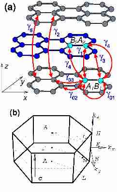
Natural graphite occurs mainly with stacking order and has four atoms in the unit cell (two atoms for each graphene plane) as shown in Fig. 1(a). Each atom contributes one electron to the four electronic energy bands in the 3D Brillouin zone (BZ) [see Fig. 1(b)]. FLG has parallel graphene planes stacked in an fashion above one another; the unit cell of FLG is 2D and the number of bands in the 2D BZ equals . For graphite and FLG the TB calculations are carried out with a new 3NN Hamiltonian and in addition with the well–known SWMC Hamiltonian rabi82-swmc that is valid in the vicinity to the Fermi level (). The TB parameters that enter these two Hamiltonians are for the 3NN Hamiltonian [shown in Fig. 1(a)] and for the SWMC Hamiltonian. The hopping matrix elements for the SWMC Hamiltonian are not shown here but they have a similar meaning with the difference that only one nearest neighbour in–plane coupling constant is considered (see e.g. Ref. dresselhaus81 for an explanation of SWMC parameters). The hopping matrix elements for the 3NN Hamiltonian are shown in Fig. 1(a). The atoms in the 3D unit cell are labelled , for the first layer and , for the second layer. The atom lies directly above the atom in direction (perpendicular to the layers). Within the plane the interaction is described by (e.g. and ) for the nearest neighbours, and and for second nearest and third nearest neighbours, respectively. A further parameter, (), is needed to couple the atoms directly above each other (in direction). The hopping between adjacent layers of sites that do not lie directly above each other is described by () and ( and ). The small coupling of atoms in the next–nearest layer is ( and ) and ( and ).
The calculation shown here is valid for both graphite and FLGs with small adjustment as indicated when needed. The lattice vectors for graphite in the plane are and and the out–of–plane lattice vector perpendicular to the layers is .
| (1) |
The C–C distance and the distance of two graphene layers . For a FLG with layers and hence atoms only the 2D unit vectors and . Similarly the electron wave vectors in graphite have 3 components and in FLG . A TB method (or linear combination of atomic orbitals, LCAO) is used to calculate the bare energy band and QP dispersion by two different sets of interatomic hopping matrix elements. The electronic eigenfunction is made up from a linear combination of atomic orbitals which form the electronic bands in the solid. The electron wave function for the band with index is given by
| (2) |
Here is the electronic energy band index and in the sum is taken over all atomic orbitals from atoms ,,. Note that for 3D graphite we have . The are wave function coefficients for the Bloch functions . The Bloch wave functions are given by a sum over the atomic wave functions for each orbital in the unit cell with index () multiplied by a phase factor. The Bloch function in graphite for the atom with index is given by
| (3) |
where is the number of unit cells and denotes atomic wave functions of orbital . In graphite the atomic orbital in the unit cell with index () is centered at and in FLGs at .
For the case of FLGs ) contains only the sum over the 2D in–plane . The Hamiltonian matrix defined by and the overlap matrix is defined by . For calculation of and , up to third nearest neighbour interactions (in the plane) and both nearest and next–nearest neighbour planes (in direction) are included as shown in Fig. 1(a). The energy dispersion relations are given by the eigenvalues and are calculated by solving
| (4) |
In the Appendix, we show the explicit form of for graphite FLGs with 1-3 layers.
| Method | |||||||||||||
|---|---|---|---|---|---|---|---|---|---|---|---|---|---|
| 3NN TB- | -3.4416 | -0.7544 | -0.4246 | 0.2671 | 0.0494 | 0.0345 | 0.3513 | -0.0105 | 0.2973 | 0.1954 | 0.0187 | -2.2624 | 0.0540222We adjusted the impurity doping level in order to reproduce the experimental value of . |
| 3NN TB-LDA | -3.0121 | -0.6346 | -0.3628 | 0.2499 | 0.0390 | 0.0322 | 0.3077 | -0.0077 | 0.2583 | 0.1735 | 0.0147 | -1.9037 | 0.0214 |
III SWMC Hamiltonian
The SWMC Hamiltonian has been extensively used in the literature dresselhaus81 . It considers only first nearest neighbour hopping and is valid close to the axis of graphite. For small measured from the axis (up to 0.15 ) both, the 3NN and the SWMC Hamiltonians yield identical results. The eight TB parameters for the SWMC Hamiltonian were previously fitted to various optical and transport experiments dresselhaus81 .
For the cross sections of the electron and hole pockets analytical solutions have been obtained and thus it has been used to calculate the electronic transport properties of graphite. Thus, in order to provide a connection to many transport experiments from the past, we also fitted the LDA and calculations to the SWMC Hamiltonian.
The TB parameters are directly related to the energy band structure. E.g. is proportional to the Fermi velocity in the plane and gives the bandwidth in the direction. The bandwidth of a weakly dispersive band in that crosses approximately halfway in between and is equal to , which is responsible for the semi metallic character of graphite. Its sign is of great importance for the location of the electron and hole pockets: a negative sign brings the electron pocket to while a positive sign brings the electron pocket to . There has been positive signs of reported earlier dresselhaus64-ibm but it has been found by M.S. Dresselhaus I9 ; dresselhaus81 that the electron(hole) pockets are located at () which is in agreement with recent DFT calculations alex06-correlation , tight–binding calculation charlier91-graphite and experiments dresselhaus81 ; lanzara06-graphite . The magnitude of determines the overlap of electrons and holes and the volume of the Fermi surface. It thus also strongly affects the concentration of carriers and hence the conductivity and free charge carrier plasmon frequency. The effective masses for electrons and holes of the weakly dispersive energy band are denoted by and , respectively. Their huge value also results from the small value of and causes the low electrical conductivity and low plasmon frequency in the direction perpendicular to the graphene layers since () enters the denominator in the expression for the Drude conductivity (free carrier plasmon frequency). determines the strength of the trigonal warping effect ( gives isotropic equi–energy contours) and the asymmetry of the effective masses in valence band (VB) and conduction band (CB). The other parameter from next nearest neighbour coupling, has less impact on the electronic structure: both the VB and CB at are shifted with respect to the Fermi level by causing a small asymmetry dresselhaus81 . Here is the difference in the on–site potentials at sites () and (). is the value of the gap at the point H8 . This crystal field effect for nonzero occurs in stacked graphite and FLGs but it does not occur in stacked graphite and the graphene monolayer. The small on–site energy difference appears in the diagonal elements of . It causes an opening of a gap at the point which results in a breakdown of Dirac Fermions in graphite and FLGs with . Finally, is set in such a way that the electron and hole like Fermi surfaces of graphite yield an equal number of free carriers. is measured from the bottom of the CB to the Fermi level.
| Method | ||||||||
|---|---|---|---|---|---|---|---|---|
| TB-333This work | 3.053 | 0.403 | -0.025 | 0.274 | 0.143 | 0.030 | -0.025 | -0.005444We adjusted the impurity doping level to reproduce the experimental value of |
| TB-LDAa | 2.553 | 0.343 | -0.018 | 0.180 | 0.173 | 0.018 | -0.022 | -0.018 |
| EXP555Fit to Experiment, M.S. Dresselhaus et al dresselhaus81 | 3.16 | 0.39 | -0.02 | 0.315 | 0.044 | 0.038 | -0.024 | -0.008 |
| LDA666Fit to LDA, J.C. Charlier et al charlier91-graphite | 2.598 | 0.364 | -0.014 | 0.319 | 0.177 | 0.036 | -0.026 | -0.013 |
| EXP777Fit to double resonance Raman spectra. L.M. Malard et al.pimenta07-bilayer | 2.9 | 0.3 | - | 0.1 | 0.12 | - | - | |
| KKR888Fit to Korringa-Kohn-Rostocker first principles calculation Tatar and Rabi rabi82-swmc | 2.92 | 0.27 | -0.022 | 0.15 | 0.10 | 0.0063 | 0.0079 | -0.027 |
|
|
 |
|
 |
 |
 |
 |
 |
IV Numerical fitting procedure
The ab–initio calculations of the electronic dispersion are performed on two levels: bare band dispersion calculation by LDA and QP dispersion calculations within the approximation. We calculate the Kohn-Sham band-structure within the LDA to density-functional theory (DFT) abinit . Wave-functions are expanded in plane waves with an energy cutoff at 25 Ha. Core electrons are accounted for by Trouiller-Martins pseudopotentials.
We then employ the approximation using a plasmon-pole approximation for the screening hybert86 ; hedin65-gw ; louie-gw to calculate the self-energy corrections to the LDA dispersion. For the calculation of the dielectric function we use a 15155 Monkhorst-Pack sampling of the first BZ, and conduction band states with energies up to 100 eV above the valence band (80 bands), calculations were performed using the code YAMBO self . The details for the first principles calculations are given elsewhere claudio08 .
For the fitting of the TB parameters to the ab–initio (LDA and ) calculations we used energies of the four bands of graphite at 100 points. The points were distributed inside the whole 3D BZ of graphite. The fitting was performed with the 3NN Hamiltonian. In addition we chose a smaller subset of points inside a volume of and fitted the SWMC parameters, which is frequently used in the literature dresselhaus81 ; rabi82-swmc ; partons06-graphite ).
The set of TB parameters were fitted by employing a steepest–descent algorithm that minimizes the sum of squared differences between the TB and the ab–initio calculations. This involves solving Eq. 4 with different sets of TB parameters so as to approach a minimum deviation from the ab–initio calculations. Points close to were given additional weight so that the band crossing was described with a deviation less than 1 meV. This is important for an accurate description of the Fermi surface. In Table 1 we list the parameters for the 3NN Hamiltonian that can be used to calculate TB- bands in the whole 3D BZ of graphite.
The parameters that were fit with the SWMC Hamiltonian are summarized in Table 2. These TB parameters reproduce the bare energy band (fit to LDA) and the QP (fit to ) calculated dispersions. Hereafter these fits are referred to as TB-LDA and TB-, respectively. We also list the values from other groups that were fit to experiments dresselhaus81 and to LDA charlier91-graphite and another first–principles calculation rabi82-swmc . It can be seen that the TB- parameters for the nearest neighbour coupling increase by about 20% when compared to TB-LDA. TB- is also closer to the experimental TB parameters than the TB-LDA parameters. This indicates that electronic correlation effects play a crucial role in graphite and FLGs for interpreting and understanding experiments that probe the electronic energy band structure.
V Comparision of the bare energy band to the quasiparticle dispersion of graphite
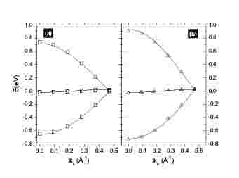
We now compare the calculated TB-LDA to TB- and we also show the result of the first–principles calculations that were used for fitting in order to illustrate the quality of the fit. In Fig. 2 the full dispersion from to for (a) TB-LDA is compared to (b) TB- calculations. It is clear that the bandwidth in increases by about 20% or 200 meV when going from TB-LDA to TB-GW, i.e. when long–range electron–electron interaction is taken into account. Such an increase in bandwidth is reflected by the TB parameter (in the SWMC model is the total bandwidth in the out–of–plane direction). It can be seen that the conduction bandwidth increases even more than the valence bandwidth. The VB dispersion was measured directly by ARPES and gave a result in good agreement to the TB- alex06-correlation .
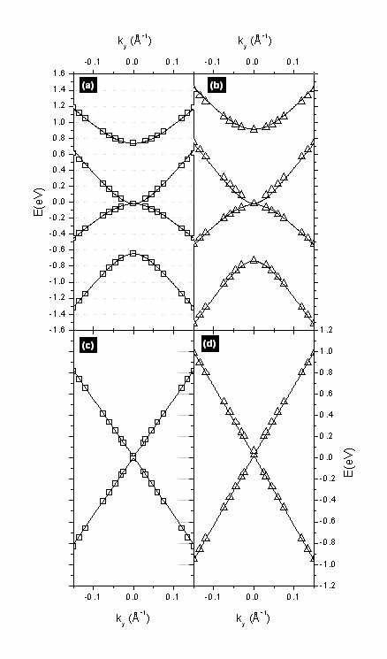
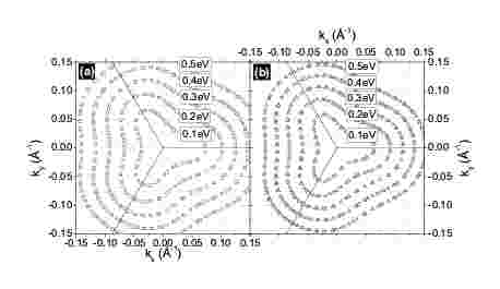
The dispersion parallel to the layers is investigated in Fig. 3 where we show the dispersion for () and (). Here the TB-GW bands also become steeper by about 20% when compared to TB-LDA. This affects which is the in–plane nearest–neighbour coupling (see Fig. 1)(a). It determines the in–plane and in–plane bandwidth which is proportional to (or proportional to in the SWMC Hamiltonian). In Fig. 4 the trigonal warping effect is illustrated by plotting an equi–energy contour for with (a) TB-LDA and (b) TB-. The trigonal warping effect is determined by which is larger in the TB- fit compared to the TB-LDA.
VI The three dimensional quasiparticle dispersion and doping dependent Fermi surface of graphite
| Point | Method | ||||
|---|---|---|---|---|---|
| -9.458 | -7.257 | 12.176 | 12.541 | ||
| TB- | -9.457 | -7.258 | 12.184 | 12.540 | |
| -3.232 | -2.441 | 1.655 | 2.491 | ||
| TB- | -3.216 | -2.457 | 1.656 | 2.495 | |
| -0.736 | -0.025 | -0.025 | 0.917 | ||
| TB- | -0.728 | -0.024 | -0.024 | 0.909 | |
| 0.020 | 0.020 | 0.025 | 0.025 | ||
| TB- | 0.020 | 0.020 | 0.025 | 0.025 |
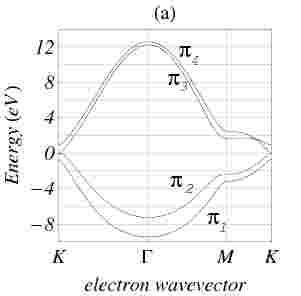
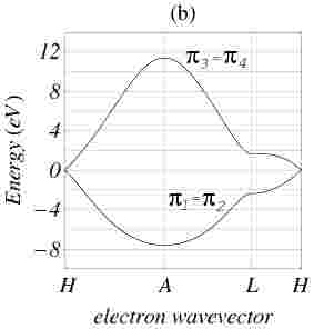
In the previous section we have shown that the bandwidth increases by 20% when going from TB-LDA to TB-. This affects especially the optical properties such as the transition that plays an important role in optical absorption and resonance Raman and thus one has to use TB- for proper description of the electronic structure of graphite including electron–electron correlation effects. In Fig. 5 we show the complete in–plane QP band structure for (a) ( point) and (b) ( point) calculated by the 3NN TB Hamiltonian. In the plane two valence bands ( and ) and two conduction bands ( and ) can be seen and in the whole plane the two valence (conduction) bands are degenerate. The ab-initio values are compared to the 3NN TB- calculation in Table 3. It can be seen that the fit reproduces the ab–initio calculations with an accuracy of 10 meV in the BZ center and an accuracy of 1 meV along the axis, close to .
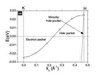
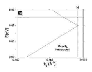
Close to the 3NN Hamiltonian is identical to the SWMC Hamiltonian. Thus, for evaluation of the Fermi surface and the doping dependence on in the dilute limit, we use the SWMC Hamiltonian. The weakly dispersing band that crosses is responsible for the Fermi surface and the electron and hole pockets. This energy band is illustrated in Fig.6(a) where we show that the TB- fit has an accuracy of 1 meV. The minority pocket that is a result of the steeply dispersive energy band close to is shown in Fig.6(b).
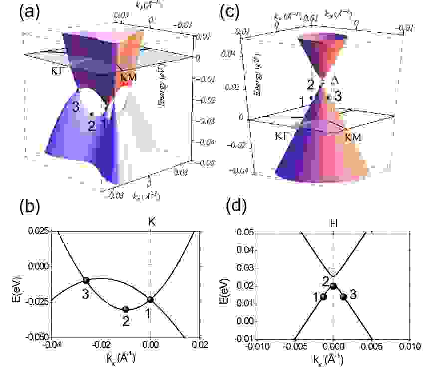
The QP dispersion close to is shown in Fig.7 for (a,b) , (c,d) point. The dispersion around the point is particular complicated: there are four touching points between valence and conduction bands. Three touching points between the valence and conduction bands exist in the close vicinity to at angles of , and away from (i.e. the direction). The fourth touching point is exactly at point. The touching points arise from the semi metallic character of graphite: there are two parabolas (VB and CB) that overlap by about 20 meV. For example the bottom of the CB is denoted by the point in Fig.7(a) and (b). At point shown in Fig.7(c) and (d) the energy band structure becomes simpler: there are only two non–degenerate energy bands and their dispersion is rather isotropic around (the trigonal warping effect in the plane is a minimum in the plane and a maximum in the plane). It is clear that the energy bands do not touch each other and the dispersion is not linear but parabolic with a very large curvature (and hence a very small absolute value of the effective mass; see Fig. 8) at . lies 20 meV below the top of the VB and the energy gap is equal to 5 meV. It is interesting to note that the a larger value of would bring the top of the VB above . The horizontal cuts through the dispersions in Fig.7 at (blue area) give cross sectional areas of an electron–like Fermi surface at () and a hole–like Fermi surface at ( point), consistent with a semi-metallic behaviour.
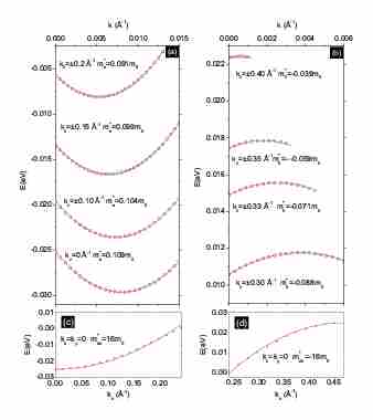
The effective in–plane massses for electrons () and holes () are evaluated along the parabola indicated in Fig.7 by the points . This parabola lies in the plane spanned by and and can thus be considered an upper limit for the effective mass since the dispersion is flat in this direction as can be seen in Fig.7(a). For the center of the parabola is chosen to be the bottom of the CB, i.e. point in Fig.7(a). Similarly for the center of the parabola is chosen to be the top of the VB, i.e. point in Fig.7(b). Due to the larger curvature of the hole bands, the absolute value of is larger than . The dependence of and is shown in Fig.8(a) and (b), respectively. For the effective mass in the direction we fit a parabola for the weakly dispersing band in direction perpendicular to the layers and get and for the effective electron and hole masses perpendicular to the layers, respectively. The Fig.8(c) and Fig.8(d) shows the TB- along for the electron and hole pocket, respectively. The parabolic fits that were used to determine the effective masses are shown along with the calculation.
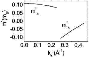
The dependence of and are shown in Fig. 9. For this purpose we evaluated the heavy electron mass of the parabolic sub bands as shown in Fig. 7 and Fig. 8). It is clear that has a weak dependence and strongly depends on the value of . This is obvious since exactly at point, the value of has a minimum. For a finite value of the gap , the value of also remains finite.
We now discuss the whole 3D Fermi surface. The volume inside the surface determines the low–energy free carrier plasmon frequencies and the electrical conductivity. The trigonal warping has little effect on the volume inside the electron and hole pocket. When we set , then the Fermi surface is isotropic around axis. The simplification of results in little change of the volume. For , there are touching points of the electron–like and hole–like Fermi surfaces dresselhaus81 . The touching points (or legs) are important for understanding the period for de–Haas–van Alphen and the large diamagnetism in graphite mikitik06-swmc . However, for the calculation of the number of carriers, they are not crucial and thus the Fermi surface calculated with can be used for the evaluation of the electron density, , and the hole density, . In this case, the cross section of the Fermi surface A() has an analytical form. The number of electrons per is given by with where is the electron pocket volume and the BZ volume. is the unit cell volume in . Similarly, by replacing with (the volume of the whole pocket) one can obtain the number of holes per . The critical quantities are and and they are obtained by integrating the cross section of the Fermi surface, along . The analytical expression and their dependence on the TB parameters is given in I9 . This yields plasmon frequencies of for plasmon oscillation parallel to the graphene layers and for plasmon oscillation perpendicular to the layers. Here venghaus75-epsilon and palmer91-hreels are adopted for the dielectric constants parallel and perpendicular to the graphene layers, respectively. We have made two simplifications: first we do not consider a finite value of temperature ( and are the plasmon frequencies at 0 K) and second we used an effective mass averaged over the whole range of the pockets as shown in Fig.8 and in Fig.9.
 |
 |
.
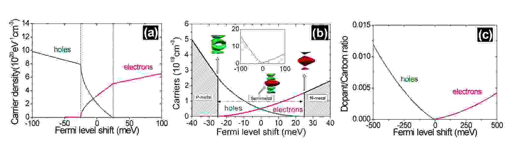
Next we discuss the doping dependence of the electronic properties in the so–called dilute limit, which refers to a very low ratio of dopant/carbon atoms. Here we use a method described previously I9 employing the TB- parameters from Table 2. This allows us to calculate the doping dependence of and . The analytical formula for the dependent cross section of the Fermi surface, (given in I9 ) is integrated for different values of . By integrating along we obtain the carrier density per eV. The ratio of dopant to carbon is given by where for electron doping and for hole doping. Here is the charge transfer value per dopant atom to Carbon. Although there are some discussions about the value of , it is was recently found for potassium doping that alex08-kc8 . In Fig. 10(a) we show the doping dependence of the carrier densities. It is clear that at , we have a discontinuity in the carrier density and this is associated to the at which the electron or hole pocket is completely filled. Since the density of states decreases suddenly after the pockets are filled, the kink in the density of states appears. This also marks the transition from a two–carrier regime to a single–carrier regime. In Fig. 10(b) we show and . It is clear that at the number of holes equals the number of electrons. At , we have no more holes and thus a transition from a semi metal to a metal occurs. In such a metal, the carriers are electrons, hence an N–type metal. Similarly, at meV we have no more electrons and the a semi metal to metal transition occurs in the other direction to . For this metal, the carriers are holes, hence a P–type metal. These semi metal to metal transitions are important for ambipolar transport in graphite and graphene: they determine the region for the gate voltage in which ambipolar transport is possible. Finally in Fig. 10(c) we plot the ratio of dopant to carbon atoms as a function of .
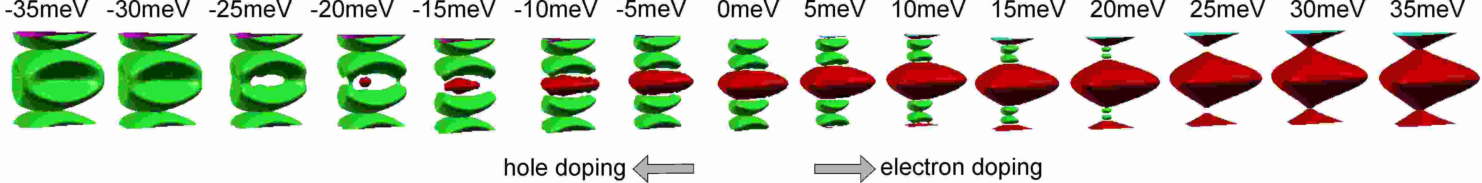
It is certainly interesting to monitor the doping induced changes in and also in the shape of the Fermi surface. In Fig.11 we show the Fermi surfaces for electron doping and hole doping for to in steps of 5 meV. It is clear that at a single carrier regime dominates as indicated by the two different colors (red for electrons and green for holes). This is consistent with Fig. 10(b) where the integrated electron (hole) densities disappear at ().
| Parameter | Symbol | TB- | Experimental value(s) |
|---|---|---|---|
| Fermi velocity at [ms-1] | 1.01 | 0.91 lanzara06a-graphite , 1.06 alex06-correlation , 1.07 andrei07-ll , 1.02 orlita08-gap | |
| Splitting of bands at [eV] | 0.704 | 0.71 alex06-correlation | |
| Bottom of band at point [eV] | E() | 7.6 | 8 takahashi06-prl , 8 law86-graphite |
| in–plane electron mass [] | 0.1 ( averaged) | 0.084 mendez79-effective_massa , 0.42 lanzara06a-graphite ,0.028 andrei07-ll | |
| in–plane hole mass []999To compare different notations, we denote here the absolute value of . | 0.06 ( averaged) | 0.069 lanzara06a-graphite , 0.03 Galt56-mass 101010Mass at the point was measured. Note that this is in excellent agreement to our calculated dependence of (see Fig. 9)., 0.028 andrei07-ll | |
| out–of–plane electron mass [] | 16 | - | |
| out–of–plane hole mass [] | -16 | - | |
| number of electrons at =0 [ cm-3] | 5.0 | 8.0 lanzara06a-graphite , 3.1 soule58-mass | |
| number of holes at =0 [ cm-3] | 5.0 | 3.1 lanzara06a-graphite , 2.7 soule58-mass , 9.2 takahashi06-prl | |
| Gap at point [meV] | 5 | 5-8 orlita08-gap ; H8 | |
| in–plane plasmon frequency [meV] | 113 | 128 geiger71-plasmon | |
| out–of–plane plasmon frequency [meV] | 19 | 45-50 palmer91-hreels ; geiger71-plasmon ; palmer96-damping1 | |
| optical transition energy [eV] | 0.669 | 0.722 J46 111111The difference between the experimental and the TB- value might be a result of excitonic effects. | |
| optical transition energy [eV] | 0.847 | 0.926 J46 b |
VII Few layer graphene
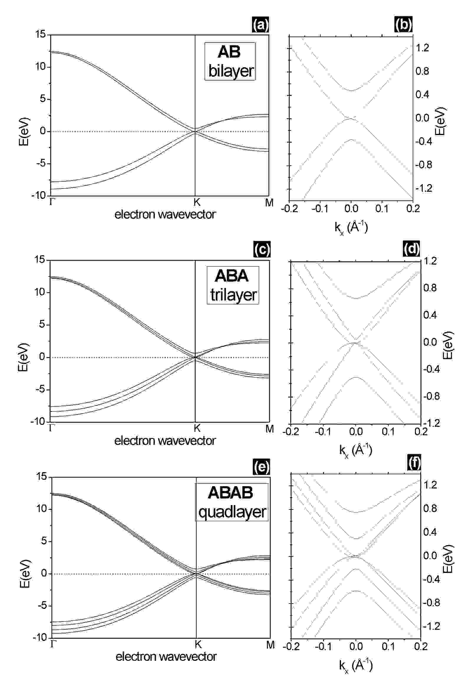
The 3NN TB- set of parameters fits the whole range of the 3D graphite BZ. Thus the set can be transferred for the calculation of QP dispersions of stacked FLGs with layers (). The transferability of TB parameters is a result of the fact that the lattice parameters of FLGs and graphite are almost identical trickey92-bilayer . We can use the matrix elements shown in Fig. 1(a) also for FLGa; for only , and are needed and this results in the graphene monolayer case. For the parameters and are not needed since they describe next nearest neighbour interactions which do not exist in a bilayer. We use the set of TB parameters given in Table 1 and the Hamiltonians given in section 2 and the appendix. In Fig. 12 we show the bilayer (), the trilayer () and the quadlayer () calculated with TB-. The Fig. 12(a) and (b) shows the electron dispersion of the bilayer. The separation between CB (VB) to the Fermi level is proportional to mccann06-bilayer and thus it is clear that the TB- also gives an about 20% larger separation between the VB than LDA. Furthermore the slope of all bands becomes steeper for TB- since increase with respect to LDA calculations. This is also responsible for the increase in of FLGs (similar to the graphite case, when going from LDA to ). The same argument is the case for the tri– and the quadlayer. It is interesting that the QP dispersion measured by ARPES rotenberg06-graphite_bilayer are in better agreement with the TB- rather than the LDA calculations performed.
The low energy dispersion relation of FLGs are particularly important for describing transport properties. From the calculations, we find that all FLG has a finite density of states at . The trilayer has a small overlap at point between valence and conduction band (i.e. semi–metallic). This property might be useful for devices with ambipolar transport properties. Our results are in qualitative agreement with the LDA calculations henrard06-hpoint .
It can be seen that a linear (Dirac–like) band appears for the trilayer (and also for all other odd-numbered multilayers). This observation is in agreement to previous calculations and is relevant to a increase in the orbital contribution to diamagnetism ando08-magnetism .
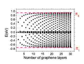
Since TB allows for rapid calculation of the QP bands, the transition from FLG to bulk graphite can be analyzed. Even in the case of , the solution of Eq. 4 for the Hamiltonian and overlap matrices takes only 10 sec on a Pentium III workstation per point. In Fig. 13 we show the eigenvalue spectrum for FLG with . As we increase and hence the number of bands, the bandwidth also increases and approaches that of bulk graphite. It can be seen that for , the total bandwidth is that of bulk graphite. Interestingly, the energies of the bands group together and form families of the highest, second highest etc. energy eigenvalue at . With increasing number of layers, a given family approaches the limit for bulk graphite. Such a family pattern is a direct consequence of the stacking sequence in FLG and it might be accessible to optical spectroscopy similar to the fine structure around point that has been observed in bulk graphite J46 .
VIII Discussion
We first discuss the QP band structure and relation to recent ARPES experiments. From several experimental works it is clear that the LDA bands need to be scaled in order to fit the experiments rotenberg06-graphite ; zhou05-graphite ; alex06-correlation . Our new set of TB parameters quantitatively describes the QP dispersions of graphite and FLG. The scaling is mainly reflected in an increase of and , the in–plane and out–of–plane coupling, respectively. It thus can be used to analyze ARPES of both pristine and doped (dilute limit) graphite and FLG. Most importantly, the correlation effects increase , the Fermi velocity when going from LDA to . For the TB- calculation, ms-1 which is in perfect agreement to the values from ARPES that is equal to ms-1 alex06-correlation . The question why LDA works for some metals but fails to give the correct and energy band dispersion in semi metallic graphite arises. In graphite, the contribution of the electron–electron interaction to the self–energy is unusually large. The reason for this is the small number of free carriers to screen efficiently the Coulomb interaction. In most other metals, the density of states at has a much larger ( 1000 times) value than in graphite and the screening lengths are shorter. Hence the LDA is a good description for such a material but it fails in the case of graphite. Another parameter that illustrates the quality of the TB- to reproduce the experimental QP dispersion is , the band splitting at point. For TB-, we obtain eV and the ARPES gives eV alex06-correlation .
The TB parameters of the SWMC Hamiltonian have been fitted in order to reproduce double–resonance Raman spectra pimenta07-bilayer . As a result they obtained that (one of the parameters that couples the neighbouring graphene planes) has a value of 0.1 eV while the for graphite that we obtain in this paper is 0.274 eV (see Table II) and the value that was fit to transport experiments is 0.315 eV alex07-kirchberg ; dresselhaus81 which is also in perfect agreement to ARPES experiments of graphite single crystals alex07-kirchberg . We now discuss a possible reason for this discrepancy. The fitting procedure in Ref pimenta07-bilayer depends on the choice of the phonon dispersion relation of graphite. It is important to note that recently a Kohn anomaly has been directly observed by inelastic x–ray scattering experiments using synchrotron radiation alex08-ixs which has a steeper slope of the TO phonon branch at point in contrast to previous measurements maultzsch04 . Thus the assumption of the correct phonon dispersion relation is crucial for obtaining the correct band structure parameters.
Next we discuss the present QP electronic energy band structure in relation to optical spectroscopies such as optical absorption spectroscopy (OAS) and resonance Raman spectroscopy. The optical spectroscopies probe the joint density of states (JDOS) weighted with the dipole matrix elements. Peaks in the OAS are redshifted when compared to the JDOS of the QP dispersion if excitons are created. By comparing the QP dispersion with OAS experiments J46 ; e41 ; zhang87 we now estimate a value for exciton binding energies in graphite. In general many resonant states with contribute to OAS but a fine structure in OAS of bulk graphite measured in reflection geometry was observed by Misu et al. J46 which was assigned to two specific transitions around : the transition between the lower VB and states just above and the transition between the upper VB and the upper CB. The experimental energies they found were eV and eV. The TB-GW dispersion yields energies eV and eV [see Fig.2(b)]. Assuming one exciton is created for the () transition, this yields exciton binding energies of meV and meV for a point exciton in bulk graphite. Such a value for the exciton binding energies most probably increases when going from bulk graphite to FLGs due to confinement of the exciton wave function in direction.
Concerning the value of , the gap at , several experimental values exist and magneto reflectance experiments suggest =5 meV. This is in disagreement to the calculated values obtained for pristine graphite alex06-correlation . However, when the doping level is slightly increased, becomes smaller and we thus fixed a doping level in the ab–initio calculation that reproduces the experimental claudio08 . While some of the variations may be explained by the sample crystallinity in direction, it is also conceivable that small impurities are responsible for the discrepancy.
Next we discuss a possibility to measure the free carrier plasmon frequencies of the of pristine and alkali–metal doped graphite by high resolution energy electron loss spectroscopy (HREELS). The electron concentration inside the pockets very sensitively affects the plasmon frequencies. In principle the charge carrier plasmons should also appear as a dip in optical reflectivity measurements but due to the small relative change in intensity they have not been observed so far. Due to the small size of the pockets, the number of charge carriers and hence the conductivity and plasmon frequencies are extremely sensitive to temperature and doping. Experimentally observed plasmon frequencies for oscillations parallel to the graphene layers are = geiger71-plasmon and for oscillations perpendicular to the layers are = palmer91-hreels ; geiger71-plasmon ; palmer96-damping1 . These values for and agree reasonably well with our derived value considering that we make the crude estimation of and at 0 K while experiments where carried out at room temperature. We also used average effective masses of the electron pocket in order to determine the plasmon frequency, while in fact there is a dependence (see Fig.9) . We also note that the experimental literature values for and have a rather wide range, e.g. zanini77-epsilon from reflectivity measurements and venghaus75-epsilon from EELS.
The temperature dependence of was measured by Jensen et al palmer91-hreels by HREELS and they observed a strong T dependence for which was attributed to changes in the occupation and thus number of free carriers with T. The observed plasmon energy was rising from 40 meV to 100 meV in a temperature range of 100 K to 400 K. A similar effect might be observed by HREELS of doped graphite as a function of doping level. It would be interesting to study the evolution of the plasmon frequency with doping level. With our current understanding of the low–energy band structure we predict a semimetal to metal transition at a Fermi level shift of meV. At this doping level, the hole pocket is completely filled with electrons and disappears and the electron pocket has roughly doubled in size and and should increase by a factor of . Such a transition should be observable by HREELS and might be accompied by interesting changes in the band structure (electron–plasmon coupling) which can also be measured simultaneously by ARPES. Many DC transport properties can be understood with a Drude model for the conductivity, which is inversely proportional to the effective carrier mass. From the ratio of and , we hence expect that the DC electron(hole) conductivity in direction is () times less than the in–plane conductivity . The experimental value is dresselhaus81 and considering the large variation in experimental values even for the in–plane conductivity morelli84-resistivity ; dresselhaus81 , it is in reasonable agreement. In Table 4 we summarize the electronic band structure properties such as , , the effective masses etc. and compare them to experimental values.
IX Conclusions
In conclusion, we have fitted two sets of TB parameters to first principles calculations for the bare band (LDA) and QP () dispersions of graphite. We have observed a 20% increase of the nearest neighbour in–plane and out–of–plane matrix elements when going from LDA to . Comparision to ARPES and transport measurements suggest that LDA is not a good description of the electronic band structure of graphite because of the importance of correlation effects. We have explicitely shown that the accuracy of the TB- parameters is sufficient to reproduce the QP band structure with an accuracy of 10 meV for the higher energy points and 1 meV for the bands that are relevant for electronic transport. Thus the 3NN TB- calculated QP band energy dispersions are sufficiently accurate to be compared to a wide range of optical and transport experiments. The TB- parameters from Table I should be used in the future for interpretation of experiments that probe the band structure in graphite and FLG. For transport experiments that only involve electronic states close to the axis (in graphite) or the point in FLG, the SWMC Hamiltonian with parameters from Table II can be used.
With the new set of TB parameters we have calculated the low energy properties of graphite: the Fermi velocity, the Fermi surface, plasmon frequencies and the ratio of conductivities parallel and perpendicular to the graphene layers and effective masses. These values are compared to experiments and we have demonstrated an excellent agreement with almost all values.
We have shown that at meV, a semi metal to metal transition exists in graphite. Such a transition should be experimentally observable by HREELS or ARPES for electron doped graphite single crystals with very low doping levels (i.e. the dilute limit). Experimentally, the synthesis of such samples is possible by evaporation of potassium onto the sample surface and choosing a sufficiently high equilibration temperature so that no staging compound forms. It would thus be interesting to do a combined ARPES and HREELS experiment on this kind of sample.
We have also discussed the issue of the existence of Dirac Fermions in graphite and FLGs. For pristine graphite it is clear that for a finite value of the gap at point, we always have a non–zero value of the effective masses at . We now discuss some possibilities for . One way would be to use stacked graphite. However, natural single crystal graphite has mainly stacking and the preparation of an like surface by repeated cleaving is a rather difficult task. Recently, the possibility of reducing by increasing the doping level has been put forward alex08-kc8 ; claudio08 and this seems a more promising way for experiments. For the case of a fully doped graphite single crystal, the interlayer interaction is negligible because the distance between the graphene sheets is increased and the stacking sequence is change to stacking. These two effects would cause the appearance of Dirac Fermions in doped graphite.
With the new set of 3NN TB parameters we have calculated the QP dispersion of FLG in the whole 2D BZ. We have shown the evolution of the energy eigenvalue spectrum at point as a function of , the number of layers. An interesting family pattern was observed, where the first,second, third etc. highest transitions form a pattern that approaches the energy band width of bulk graphite with increasing . For the highest transition, the bulk graphite band width is already reached at . This family pattern is a direct result of the stacking sequence in FLG and it can possibly be observe experimentally. It should be pointed out here, that a very similar fine structure around the point in bulk graphite has been observed by optical absorption spectroscopy by Misu et al. J46 although the family pattern from Fig. 13 might be observed also by ARPES on high quality FLGs synthesized on Ni(111).
Acknowledgement
A.G. acknowledges a Marie Curie Individual Fellowship (COMTRANS) from the European Union. A.R. and C.A. are supported in part by Spanish MEC (FIS2007-65702-C02-01), Grupos Consolidados UPV/EHU of the Basque Country Government (IT-319 -07) European Community e-I3 ETSF and SANES (NMP4-CT-2006-017310) projects. L.W. acknowledges support from the French national research agency. R.S. acknowledges MEXT grants Nos. 20241023 and 16076201. We acknowledge M. Knupfer for critical reading of the manuscript. XCrysDen xcrysden was used to prepare Fig. 10.
Appendix
We made computer programs to automatically generate the 3NN Hamiltonians and overlap matrices for graphene layers. The method is following the description by Partoens et al. partons06-graphite but with the difference that we include 3NN matrix elements that describe the QP dispersion in the whole BZ. It is interesting to note the similarity between the Hamiltonian of a layer graphene and a stage graphite intercalation compound saito86-gic . The general form of the Hamiltonian is given by
and the overlap matrix is given by
The QP band structure is then given by solving equation Eq. 4. The 3NN TB Hamiltonians can be used with parameters from Table 1. In the following we give the explicit form for the and of a monolayer and an stacked bi– and and trilayer which was used in section VII.
Monolayer graphene
The monolayer 3NN Hamiltonian and overlap matrices are given by
and
Bilayer graphene
The bilayer 3NN Hamiltonian and overlap matrices are given by
| (9) |
and
| (14) |
Trilayer graphene
The trilayer Hamiltonian and overlap matrices read as
| (21) |
and
| (28) |
The sum of the phase factors for first–,second– and third nearest neighbours are given by , and , respectively. Note that and couple and atoms and describes the and interactions.
| (29) |
| (30) |
| (31) |
Here and are the vectors that connect the atom (see Fig. 1) with the second nearest atoms (three atoms) and the third nearest atoms (six atoms), respectively.
References
- (1) Th. Seyller, K.V. Emtsev, K. Gao, F. Speck, L. Ley, A. Tadich, L. Broekman, J.D. Riley, R.C.G. Leckey, O. Rader, A. Varykhalov, and A.M. Shikin, Surf. Sci. 600, 3906 (2006).
- (2) A. Grüneis and D. Vyalikh, Phys.Rev. B 77, 193401 (2008).
- (3) K.S. Novoselov, D. Jiang, F. Schedin, T.J. Booth, V.V. Khotkevich, S.V. Morozov, and A.K. Geim, PNAS 102, 10451 (2005).
- (4) A. Geim and K. Novoselov, Nature Mat. 6, 183 (2007).
- (5) M. I. Katsnelson, K. S. Novoselov, and A. K. Geim, Nature Phys. 2, 620 (2006).
- (6) T. Ohta, A. Bostwick, T. Seyller, K. Horn, and E. Rotenberg, Science 313, 951 (2006).
- (7) C. Berger, Z. Song, T. Li, X. Li, A.Y. Ogbazghi, R Feng, Z. Dai, A.N. Marchenkov, E.H. Conrad, P.N. First, and W.A. de Heer, J. Phys. Chem. 108, 19912 (2004).
- (8) V. M. Karpan, G. Giovannetti, P. A. Khomyakov, M. Talanana, A. A. Starikov, M. Zwierzycki, J. van den Brink, G. Brocks, and P. J. Kelly, Physical Review Letters 99(17), 176602 (2007).
- (9) A. Bostwick, T. Ohta, T. Seyller, K. Horn, and E. Rotenberg, Nature Phys. 3, 36 (2007).
- (10) A. Grüneis, C. Attaccalite, T. Pichler, V. Zabolotnyy, H. Shiozawa, S.L. Molodtsov, D. Inosov, A. Koitzsch, M. Knupfer, J. Schiessling, R. Follath, R. Weber, P. Rudolf, L. Wirtz, and A. Rubio, Phys. Rev. Lett. 100, 037601 (2008).
- (11) S. Y. Zhou, G. H. Gweon, C. D. Spataru, J. Graf, D. H. Lee, S. G. Louie, and A. Lanzara, Phys. Rev. B 71, 161403 (2005).
- (12) K. Sugawara, T. Sato, S. Souma, T. Takahashi, and H. Suematsu, Phys. Rev. Lett. 98, 036801 (2007).
- (13) S. Reich, C. Thomsen, and P. Ordejón, (2002). Phys. Rev. B 65, 153407 (2002).
- (14) L.M. Malard, J.Nilsson, D.C.Elias, J.C.Brant, F.Plentz, E.S.Alves, A.H.Castro Neto, and M.A.Pimenta, Phys. Rev. B 76, 201401 (2007).
- (15) A. Bostwick, T. Ohta, J.L. McChesney, T. Seyller, K. Horn, and E. Rotenberg, Solid State Communications 143(1-2), 63–71 (2007).
- (16) B. Partoens and F.M.Peeters, Physical Review B 74, 75404 (2006).
- (17) K. Sasaki, J. Jiang, R. Saito, S. Onari, and Y. Tanaka, J. Phys. Soc. Jpn. 76, 033702 (2007).
- (18) R.C. Tatar and S. Rabi, Physical Review B 25, 4126 (1982).
- (19) M. S Dresselhaus and G. Dresselhaus, Advances in Phys. 30, 139 (1981).
- (20) M.S. Dresselhaus and J. Mavroides, IBM Journal of Research and development page 262 (1964).
- (21) M. S. Dresselhaus, G. Dresselhaus, and J. E. Fischer, Phys. Rev. B 15, 3180–3192 (1977).
- (22) J.C. Charlier, X. Gonze, and J.P. Michenaud, Phys. Rev. B 43, 4579 (1991).
- (23) S. Y. Zhou, G. H. Gweon, J. Graf, A. V. Fedorov, C. D. Spataru, R. D. Diehl, Y. Kopelevich, D. H. Lee, S. G. Louie, and A. Lanzara, Nature Phys. 69, 245419 (2006).
- (24) W. W. Toy, M. S. Dresselhaus, and G. Dresselhaus, Phys. Rev. B 15, 4077–4090 (1977).
- (25) G. P. Mikitik and Yu. V. Sharlai, Phys.Rev. B73, 235112 (2006).
- (26) X. Gonze, J.M. Beuken, R. Caracas, F. Detraux, M. Fuchs, G.M. Rignanese, L. Sindic, M. Verstraete, G. Zerah, F. Jollet, M. Torrent, A. Roy, M. Mikami, Ph. Ghosez, J.Y. Raty, and D.C. Allan, Comput. Mater. Sci. page 478 (2002).
- (27) M .S. Hybertsen and S. G. Louie, Phys. Rev. B 34, 5390 (1986).
- (28) L. Hedin, Phys. Rev. 139, A796–A823 (1965).
- (29) S. G. Louie, Topics in Computational Materials Science, edited by C. Y. Fong (World Scientific, Singapore) page 96 (1997).
- (30) A. Marini et al., the Yambo project, http://www.yambo-code.org/.
- (31) C. Attaccalite, A. Grüneis, T. Pichler, and A. Rubio, in preparation (2008).
- (32) H. Venghaus, Phys.Stat.Sol.B 71, 609 (1975).
- (33) E.T. Jensen, R.E. Palmer, and W. Allison, Phys. Rev. Lett. 66, 492 (1991).
- (34) A. Grüneis, C. Attaccalite, A. Rubio, D. Vyalikh, S.L. Molodtsov, J. Fink, R. Follath, W. Eberhardt, B. Büchner, and T. Pichler, Nature Mat. in review ().
- (35) S. Y. Zhou, G. H. Gweon, J. Graf, A. V. Fedorov, C. D. Spataru, R. D. Diehl, Y. Kopelevich, D. H. Lee, S. G. Louie, and A. Lanzara, Nature Phys. 69, 245419 (2006).
- (36) G. Li and E. Andrei, Nature Phys. 3, 623 (2007).
- (37) M. Orlita, C. Faugeras, G. Martinez, D.K. Maude, M.L. Sadowski, and M. Potemski, Phys. Rev. Lett. 100, 136403 (2008).
- (38) K. Sugawara, T. Sato, S. Souma, T. Takahashi, and H. Suematsu, Physical Review B 73, 045124 (2006).
- (39) A.R. Law, M.T Johnson, and H.P. Hughes, Physical Review B 34, 4289 (1986).
- (40) E. Mendez, T.C. Chieu, and N. Kambe M.S. Dresselhaus, Solid State Commun. 33, 837 (1980).
- (41) J. K. Galt, W. A. Yager, and H. W. Dail, Phys. Rev. 103(5), 1586–1587 (Sep 1956).
- (42) D.E. Soule, Phys. Rev. 112, 698 (1958).
- (43) J. Geiger, H. Katterwe, and B. Schroder, Z.Phys.B 241, 45 (1971).
- (44) P. Laitenberer and R. E. Palmer, Phys.Rev.Lett. 76, 1952 (1996).
- (45) E. Mendez, A. Misu, and M. S. Dresselhaus, Phys. Rev. B 21, 827 (1980).
- (46) S.B. Trickey, F.Müller-Plathe, G.H.F. Diercksen, and J.C. Boettger, Physical Review B 45, 4460 (1992).
- (47) Edward McCann and Vladimir I. Fal ko, Phys. Rev. Lett. 96, 086805 (2006).
- (48) Sylvain Latil and Luc Henrard, Phys. Rev. Lett. 97, 036803 (2006).
- (49) Mikito Koshino and Tsuneya Ando, Physica E: Low-dimensional Systems and Nanostructures 40(5), 1014 (2008).
- (50) A. Grüneis, T. Pichler, H. Shiozawa, C. Attaccalite, L. Wirtz, S.L. Molodtsov, R. Follath, R. Weber, and A. Rubio, physica status solidi (b) 244, 4129 4133 (2007).
- (51) A. Grüneis et al., submitted (2008).
- (52) J. Maultzsch, S. Reich, C. Thomsen, H. Requardt, and P. Ordeon, Phys. Rev. Lett. 92, 75501 (2004).
- (53) A. Misu, E. Mendez, M. S. Dresselhaus, and K. Nakao, J. Phys. Soc. Jpn. 47, 199–216 (1979).
- (54) J. M. Zhang and Eklund, J.Mat.Res. 2, 858 (1987).
- (55) M. Zanini and J. Fischer, Mat.Sci.Eng. 31, 169 (1977).
- (56) D.T. Morelli and C. Uher, Phys. Rev. B 30, 1080 (1984).
- (57) A. Kokalj, Comp. Mat. Sci. 28, 155 (2003).
- (58) R. Saito and H. Kamimura, Phys. Rev. B 33(10), 7218 (1986).