Valley splitting in Si quantum dots embedded in SiGe
Abstract
We examine energy spectra of Si quantum dots embedded into Si0.75Ge0.25 buffers using atomistic numerical calculations for dimensions relevant to qubit implementations. The valley degeneracy of the lowest orbital state is lifted and valley splitting fluctuates with monolayer frequency as a function of the dot thickness. For dot thicknesses nm valley splitting is found to be eV. Using the unique advantage of atomistic calculations we analyze the effect of buffer disorder on valley splitting. Disorder in the buffer leads to the suppression of valley splitting by a factor of 2.5, the splitting fluctuates with eV for different disorder realizations. Through these simulations we can guide future experiments into regions of low device-to-device fluctuations.
Understanding and design of silicon nanometer-scaled electronic devices has regained significant interest. This interest is sparked by the experimental progress that enabled the reproducible construction of geometries in which electrons are confined in three dimensions to length scales of a few nanometers and the potential applications of this technology to ultra-scaled traditional CMOS devices. Emerging application of Si nanostructures for qubit implementations due to long spin relaxation timesKane (1998); Wilamowski et al. (2002); Tyryshkin et al. (2005) imposes additional stringent requirements on energy spectrum engineering, including the precise control of valley degeneracy. The six-fold valley degeneracy of bulk Si is reduced to two-fold degeneracy when electrons are confined to two dimensions (2D), such as at Si/SiO2 interface in mainstream MOSFETs. Already decades ago it was recognized that there is a small splitting between the two valleys in the lowest subbandAndo et al. (1982). Recently, calculations predicted that valley splitting in narrow (few nm) SiGe/Si/SiGe quantum wells can be of the order of 10-100 meV and should fluctuate rapidly with the well thicknessBoykin et al. (2004a, b); Nestoklon et al. (2006); Friesen et al. (2007). However, experimentsWeitz et al. (1996); Koester et al. (1997); Lai et al. (2004) produced valley splitting about 2 orders of magnitude smaller than that prediction, which has been explainedKharche et al. (2007) by the disorders of the Si/SiGe interface and in the SiGe buffer. The experimentsGoswami et al. (2007) and theoretical methods indicated that additional spatial confinement will minimize the role of interface disorder and increase valley splitting. In this paper we investigate the role of SiGe buffer disorder on valley splitting and answer the fundamental question of the size and controllability of valley splitting for relevant experimental structures.
Three dimensional (3D) confinement of electrons can be achieved by various techniques. Electrostatic surface gating of 2D gas provides relatively weak and smooth spatial confinement potentials. In contrast, 3D confinement by Si/SiO2 interface produces sharp potential with Coulomb energies approaching room temperatureTakahashi et al. (1995); Zhuang et al. (1998) and large valley splittingRokhinson et al. (2002). Recently, an alternative approach to 3D confinement has been demonstrated with an advantage of lithographically defined epitaxial Si/SiGe interfaces using post-fabrication regrowthBo et al. (2006). In this case spurious charging effectsRokhinson et al. (2000), related to the traps in SiO2 or unpassivated interface can be avoided, yet retaining sharp confining potential. We will simulate such defined Si nanostructures in SiGe buffers and explore sizes relevant for qubit implementations. Simulation capabilities to represent structures containing 10 million atoms explicitly enable the atomic representation of the dot, interfaces and the SiGe buffer. Atomistic simulations also present a unique opportunity to vary the amount of the buffer disorder in order to attain detailed understanding of the physics of valley splitting, including its magnitude and fluctuations. The valley splitting is primarily defined by the smallest dimension of the device and our conclusions are applicable to any Si nanostructure defined from SiGe/Si/SiGe quantum wells.
Calculations of the energy spectrum are performed using the NEMO-3D general purpose code, which represents each atom in the domain explicitly. The theory undelying the tool and its relevant benchmarks are given in Refs Klimeck et al. (2002, 2007). The structure is defined on the relaxed (001) Si0.75Ge0.25 substrate and the Keating valence-force field model is used to adjust atomic positions to minimize the strain energy. Calculations of electronic structure are based on the 20 band tight-binding model. The quantum dot was modeled as a rectangle grown on 37 nm-thick substrate and embedded into 27 nm-thick Si0.75Ge0.25 buffer, , where is along the growth direction. We investigated the influence of the buffer thickness on electronic structure, there were no significant changes for substrates nm and buffers nm.
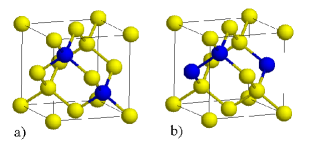
For 25% Ge we can generate various placements of Ge atoms in the Si0.75Ge0.25 buffer, with fully ordered containing only Si-Ge bonds, partially ordered containing single Ge-Ge bond per 8-atom supercell in a fixed position, and disordered having random placement of Ge atoms retaining 25% composition, see schematic in Fig. 1.
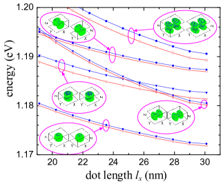
We start with the analysis of energy levels and valley splitting in a dot embedded into a fully ordered buffer. Evolution of energy levels for a nm nm dot is shown in Fig. 2 (the actual dot thickness nm monolayers). All levels come in pairs, both levels in the pair having similar wavefunction envelopes (each level is also double spin-degenerate, which has been confirmed by calculations and will be ignored for the rest of the paper). The 3D representations of the envelope wavefunctions at 20% value are shown for the lowest 6 levels. The two lowest levels have similar -type wavefunctions and represent the same orbital state with different valley number. The energy difference between them we call valley splitting . The next two levels have one node and belong to the next orbital state. For nm the -type state has lower energy than - and -type states due to the combination of sizes and effective mass anisotropy. The -type level has the highest sensitivity to , as expected, and for nm its energy becomes lower than that of the -type state. Energy separation between the ground and the first exited orbital states meV is large enough to restrict qubit Hilbert space to the lowest orbital state at low temperatures.
Valley mixing results from superposition of two counter-propagating waves reflected from the opposite Si/SiGe heterointerfaces of the dot. The phase difference of the two waves depends on the details of the interface. The strength of the mixing depends on the amplitude of the wavefunctions at the interfaces, , where is the value of the envelope of the electron wavefunction at the dot boundaryNestoklon et al. (2006). For -type and -type (top curve in Fig. 2) states wavefunctions are pushed toward -heterointerface and valley splitting for these state are significantly larger than for the ground and - or -type states.
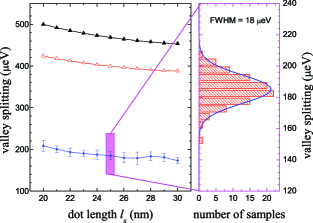
The most interesting question which can be uniquely studied by atomistic calculations is the role of buffer disorder. In Fig. 3 valley splitting of the ground level is plotted for a nm nm dot as a function of the dot size for fully ordered, partially ordered and completely disordered buffer. For fully ordered buffer the valley splitting is meV, consistent with analytical calculations. The value does not change significantly with the dot size, which confirms that valley splitting is primarily determined by the smallest dimension. For partially ordered buffers we see a reduction of by 10%, while for fully disordered buffer is reduced 2.5 times to meV. To investigate fundamental reproducibility of we performed calculations for 100 realizations of the buffer disorder for each point. The histogram of for nm dot is plotted in the right frame. The distribution is Gaussian, with standard deviation of 9.4 eV, which is % of . The bars on the main plot indicate standard deviation for other dot sizes.
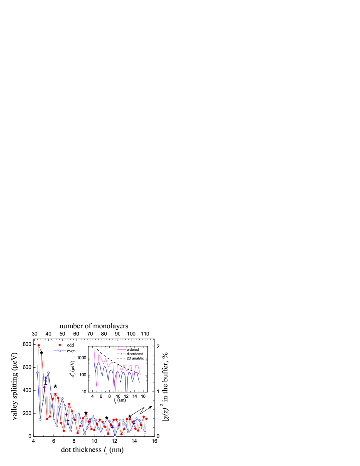
Inter-valley mixing is very sensitive to the smallest dimension of the dot, , and fluctuates with a monolayer (ML) frequency , where is the center of the valleys and is the lattice constant. Valley splitting as a function of with ML resolution is plotted in Fig. 4 (black line), and bars indicate standard deviation for different disorder realizations. It has been noted that QWs with odd and even number of MLs belong to different symmetry classesNestoklon et al. (2006). Indeed, if we connect for even and odd number of MLs we obtain two similar curves which fluctuate with a period of MLs and are out-of-phase with each other. The value of for the dot embedded into a disordered buffer is reduced by a factor of 2.5, as shown in the inset. For comparison we also plot valley splitting calculated for the 2D QW using envelope function methodNestoklon et al. (2006) (dashed line), which coincides with our calculations for the ordered buffer. Saturation of valley splitting for large , compared with the analytical dependence, is due to an additional lateral confinement. In Fig. 4 stars indicate percentage of the wavefunction which penetrates the buffer above and below the dot, the envelope of follows as a function of .
To summarize, we calculate energy levels and valley splitting for a small Si dot embedded in a disordered SiGe buffer. We find that buffer disorder leads to the suppression of valley splitting by and actual values fluctuate with standard deviation of eV. At the same time disorder limits the lowest valley splitting, which can reach zero for a perfectly ordered buffer for some dot thicknesses, and dots with valley splitting eV can be predictably designed from narrow QW ( nm).
The work was supported by ARO/LPS Award No. W911NF-05-1-0437. The use of nanoHUB.org computational resources operated by the Network for Computational nanotechnology funded by NSF is acknowledged.
References
- Kane (1998) B. Kane, Nature (London) 393, 133 (1998).
- Wilamowski et al. (2002) Z. Wilamowski, W. Jantsch, H. Malissa, and U. Rössler, Phys. Rev. B 66, 195315 (2002).
- Tyryshkin et al. (2005) A. Tyryshkin, S. Lyon, W. Jantsch, and F. Schäffler, Phys. Rev. Lett. 94, 126802 (2005).
- Ando et al. (1982) T. Ando, A. B. Fowler, and F. Stern, Rev. of Mod. Phys. 54, 437 (1982).
- Boykin et al. (2004a) T. B. Boykin, G. Klimeck, M. A. Eriksson, M. Friesen, S. N. Coppersmith, P. von Allmen, F. Oyafuso, and S. Lee, Appl. Phys. Lett. 84, 115 (2004a).
- Boykin et al. (2004b) T. B. Boykin, G. Klimeck, M. Friesen, S. N. Coppersmith, P. von Allmen, F. Oyafuso, and S. Lee, Phys. Rev. B 70, 165325 (2004b).
- Nestoklon et al. (2006) M. O. Nestoklon, L. E. Golub, and E. L. Ivchenko, Phys. Rev. B 73, 235334 (2006).
- Friesen et al. (2007) M. Friesen, S. Chutia, C. Tahan, and S. N. Coppersmith, Phys. Rev. B 75, 115318 (2007).
- Weitz et al. (1996) P. Weitz, R. Hauga, K. V. Klitzing, and F. Schaf̈fler, Surf. Sci. 361/362, 542 (1996).
- Koester et al. (1997) S. Koester, K. Ismail, and J. Chu, Semicond. Sci. Technol. 12, 384 (1997).
- Lai et al. (2004) K. Lai, W. Pan, D. C. Tsui, S. Lyon, M. Mühlberger, and F. Schäffler, Phys. Rev. Lett. 93, 156805 (2004).
- Kharche et al. (2007) N. Kharche, M. Prada, T. B. Boykin, and G. Klimeck, Appl. Phys. Lett. 90, 092109 (2007).
- Goswami et al. (2007) S. Goswami, K. Slinker, M. Friesen, L. McGuire, J. Truitt, C. Tahan, L. Klein, J. Chu, P. Mooney, D. V. der Weide, et al., Nat. Phys. 3, 41 (2007).
- Takahashi et al. (1995) Y. Takahashi, M. Nagase, H. Namatsu, K. Kurihara, K. Iwdate, Y. Nakajima, S. Horiguchi, K. Murase, and M. Tabe, Electronics Letters 31, 136 (1995).
- Zhuang et al. (1998) L. Zhuang, L. Guo, and S. Y. Chou, Appl. Phys. Lett. 72, 1205 (1998).
- Rokhinson et al. (2002) L. P. Rokhinson, D. C. Tsui, L. N. Pfeiffer, and K. W. West, Superlattices Microstruct. 32, 99 (2002), eprint cond-mat/0303011.
- Bo et al. (2006) X.-Z. Bo, L. Rokhinson, N. Yao, D. Tsui, and J. Sturm, J. Appl. Phys. 100, 94317 (2006).
- Rokhinson et al. (2000) L. P. Rokhinson, L. J. Guo, S. Y. Chou, and D. C. Tsui, Appl. Phys. Lett. 76, 1591 (2000).
- Klimeck et al. (2002) G. Klimeck, F. Oyafuso, T. Boykin, R. Bowen, and P. von Allmen, Comput. Model. Eng. Sci. pp. 601 – 42 (2002).
- Klimeck et al. (2007) G. Klimeck, S. Ahmed, H. Bae, N. Kharche, S. Clark, B. Haley, S. Lee, M. Naumov, H. Ryu, F. Saied, et al., IEEE Trans. Electron. Devices pp. 2079 – 89 (2007).