Ferromagnetism and spin polarized charge carriers in In2O3 thin films
Abstract
We present evidence for spin polarized charge carriers in In2O3 films. Both In2O3 and Cr doped In2O3 films exhibit room temperature ferromagnetism after vacuum annealing, with a saturation moment of approximately 0.5 emu/cm3. We used Point Contact Andreev Reflection measurements to directly determine the spin polarization, which was found to be approximately 505% for both compositions. These results are consistent with suggestions that the ferromagnetism observed in certain oxide semiconductors may be carrier mediated.
pacs:
75.50.Pp, 75.25.MkThe potential technological applications of magnetic semiconductors to the field of spintronics have motivated the study of many promising systems, including (Ga,Mn)As macdonald ; R1 and transition metal doped semiconducting oxides (DMSO)coeyB ; chambers . Some of these latter systems have been predicted to exhibit room temperature ferromagnetismohno , which has been observed experimentally in Co doped TiO2cotio , Co doped ZnOcozno , and Cr doped In2O3moodera . However, the origin of ferromagnetism in these DMSO materials remains enigmatic, in part because of the possibility of a magnetic signal arising from undetected transition metal oxide impurity phasesimpurity . At the same time, ferromagnetism has been observed in a number of undoped oxide samples including HfO2hfo2 , TiO2tio2 , In2O3tio2 . The recent results on ferromagnetism in carboncarbon emphasizes the importance of vacancies and other defects in promoting ferromagnetic order.
In2O3 is a transparent semiconductor and can be highly conductive at room temperature when doped, making ferromagnetic In2O3 films attractive candidates for magneto-optical and spintronic devices. Room temperature ferromagnetism has been predicted for Mo doped In2O3 films moio and observed in Ni, Fe, and Co doped samples tmdoped as well as undoped In2O3tio2 . It has been shown that the electrical and magnetic properties of Cr:In2O3 films are both sensitive to the oxygen vacancy defect concentration, and that the ferromagnetic interaction depends on carrier densitymoodera . While it has been suggested that ferromagnetism in Cr:In2O3 films is carrier mediatedzunger3 , the precise relationship between the spin transport properties of the charge carriers and the net ferromagnetic moment remains unclear.
In this Letter we demonstrate that the charge carriers in undoped In2O3 films have a significant spin polarization at helium temperatures. Furthermore, measurements on Cr doped In2O3 samples yield quantitatively similar results to measurements on undoped samples, suggesting that transition metal dopants may not play any significant role in the development of ferromagnetic order.
We prepared ceramic samples of In2O3 (with a base purity of 99.99%) and In2O3 doped with 2 at% Cr using a standard solid state processkharelcio . The powder samples were pressed into 2” diameter sputtering targets, then annealed in air at 1100 ∘C for 6 hours. In2O3 and Cr:In2O3 thin films were deposited by reactive magnetron sputtering of this target using an RF power source. High-purity argon was used as the sputtering gas and a small partial pressure of oxygen was maintained to obtain stoichiometric films. Oxygen at a partial pressure of 10-3 torr and argon at a partial pressure of 1.4x10⁻² torr were used as reactive and sputtering gases respectively. The films were deposited onto (0001) oriented single crystal sapphire substrates. While the as-prepared samples were insulating and non-magnetic, the films became conducting and ferromagnetic when annealed in vacuum for 6-8 hours.

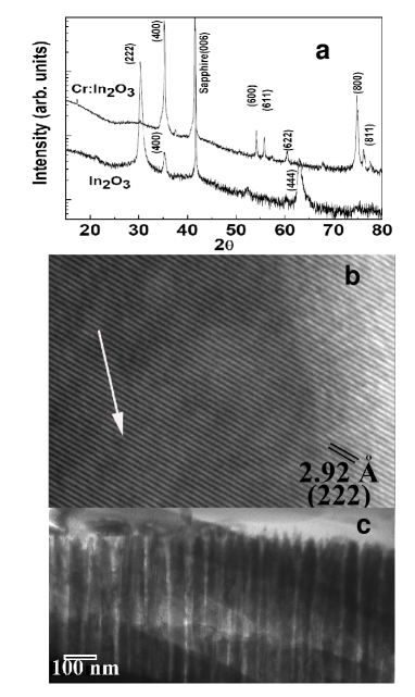
The X-Ray Diffraction (XRD) spectra for the In2O3 and Cr:In2O3 samples, are shown in Figure 1a. The polycrystalline films are textured, with strong diffraction peaks indicating a preferred orientation along (222) or (400). There is no evidence for secondary phase formation. We show high resolution (HR) and cross-sectional transmission electron microscope (TEM) images of a Cr:In2O3 film in Figs 1b and 1c. The HRTEM image shows the absence of defects, secondary phases, or clusters in these high-quality samples. Extensive SEM EDS mapping of the In2O3 films (not shown) gave no indication of any transition metal dopants, including Cr, Co, Fe, Ni, and Mn, thus ruling out the possibility of accidental contamination with magnetic transition metal impurities.

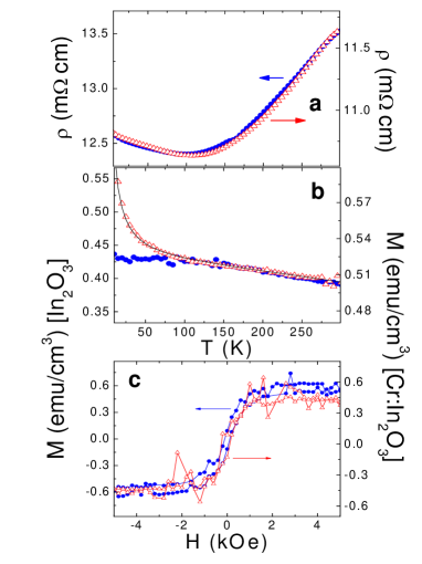
We plot the temperature dependent electrical resistivity for both the In2O3 and Cr:In2O3 samples in Fig. 2a. These data were obtained on 1.1 m thick samples after vacuum annealing. Room temperature Hall measurements estimate the carrier concentration to be 6.11019cm-3 for the In2O3 films and 3.5 1020cm-3 for the Cr:In2O3 films. Both the In2O3 and Cr:In2O3 films remain conductive down to low temperatures, and exhibit qualitatively identical behavior. This indicates that the electronic properties of both these films are very similar.
We measured the in-plane magnetization of these thin film samples using a high-sensitivity Quantum Design MPMS magnetometer. These magnetic data have been corrected for a small diamagnetic background from the sapphire substrate. The magnetization of the as-prepared samples was negligible, but a sizeable magnetic moment developed on vacuum annealing. We plot the temperature dependent magnetization for the vacuum annealed In2O3 and Cr:In2O3 films in Fig. 2b. The magnetizations for both samples exhibit very similar behavior and are almost temperature independent at higher temperatures, with the Cr:In2O3 sample showing a noticeable increase only at temperatures below 25 K. We attribute this upturn to a Curie tail arising from paramagnetic Cr ions in the sample, which are absent in the In2O3 film. Fitting this upturn to a Curie susceptibility plus a spin-wave term as:
| (1) |
with M0 a constant background, a Curie term, and the spin-wave stiffness, as shown in Fig. 2b, we find that this anomaly can be accounted for by 75% of the Cr ions remaining paramagnetic. This is consistent with our observation that ferromagnetic order can develop in oxygen deficient In2O3 in the absence of any magnetic dopants. The Curie temperature estimated from the fit using Eq. (1) is approximately TC=630 K. We plot the room temperature magnetization curves for vacuum annealed In2O3 and Cr:In2O3 films in Fig. 2c. Both samples exhibit clear hysteresis loops, consistent with room temperature ferromagnetic order. Both the In2O3 and Cr:In2O3 films show a saturation magnetization of approximately 0.50.1 emu/cm3.
In order to investigate the coupling between the charge carriers and the ferromagnetic moment in the In2O3 and Cr:In2O3 films we used PCAR spectroscopy to probe the spin polarization. PCAR spectroscopyR3 ; R4 has recently emerged as a viable technique to directly measure the transport spin polarization in magnetic materialsR2 ; R5 including various magnetic oxidesR6 , as well as the dilute magnetic semiconductorsR7 ; R8 .

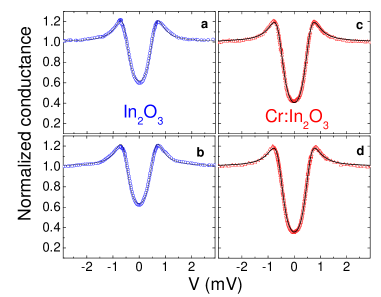
All of the measured Sn/In2O3 and Sn/Cr:In2O3 contacts exhibit characteristic conductance curves, with the dip at zero bias voltage indicating the suppression of Andreev reflection to spin polarization of the current. Figure 3 shows representative conductance curves for two different contacts for both samples. The data are analyzed using the actual BCS gap of bulk Sn, which at the measurement temperature of T=1.3 K is approximately 0.57 meV. As the typical spreading resistance of the films - in the range of 20-40 at 2 K- is comparable to the point contact resistance, which has an upper limit of 100 Ohm, this additional contribution has been included in our analysis R12 . We have estimated the minimum interfacial barrier strength value, , based on the Fermi velocity mismatch between the superconductor () and Cr:In2O3 (), . Assuming a free electron gas model and taking the effective mass to be 0.3 me moodera and the measured electron density cm-3; the Fermi velocity of Cr:In2O3 is calculated cm/s, whereas is approximately cm/s resulting in the estimated values of of , in agreement with the experimental data for Cr:In2O3 samples.
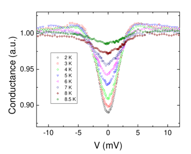
Using the free electron approximation we have estimated the mean free path for the resistivity measured at =2 K, 10.8 mcm for the Cr:In2O3 sample. Using the same resistivity value and a typical value for the contact resistance of 50 Ohm, we estimate the contact size R11 to be two orders of magnitude larger than . This implies that so that all of our measurements have been done in the pure diffusive regime. Accordingly, we have used the diffusive limit of Ref. R10 to analyze our data. This analysis, averaged over a number of different point contacts in several samples, yields a spin polarization of and in the In2O3 and Cr:In2O3 samples respectively. In order to investigate the temperature dependence of the spin polarization at low temperatures, we have also performed a series of measurements in In2O3 at different temperatures using a Nb tip. The data, shown in Figure 4, show that the magnitude of the zero bias dip decreases as the superconducting transition temperature for Nb is approached (Fig. 4). From these measurements, we calculated a spin polarization of at T=2 K in good agreement with the results obtained using the Sn tip. This value of the spin polarization is approximately independent of temperature up to T=8 K. As the temperature approaches Tc of Nb ( 9K) the fluctuations become too large to fit reliably.

The observation of carrier-mediated ferromagnetism coexisting with n-type conductivity in In2O3 poses a serious theoretical challenge. While it has been established that oxygen vacancies are the most abundant intrinsic (donor) defects in In2O3 and can account for its room-temperature conductivity Zunger1 , they alone are unlikely to produce ferromagnetism.Zunger2 Recent theoretical calculationszunger3 may explain the development of magnetic order in Cr:In2O3 but do not explain the magnetism in undoped In2O3. It has been proposed that cation vacancies could be responsible for the observed ferromagnetic properties of nonmagnetic oxides.Zunger2 ; Sawatsky ; Sanvito These defects have a tendency to form high spin magnetic states that maintain ferromagnetic interaction at relatively large distances. The spin value of the cation vacancy depends on the charge state of the defect, with neutral (q=0) and negatively charged (q=-1) indium vacancies forming S=3/2 and S=1 (triplet) states respectively. The effect is quite similar to what has been observed in thin films of liquid oxygen where two out-of surface oxygen orbitals form triplet states, which interact ferromagnetically. oxygenB
These assumptions suggest the following schematic picture. We propose that vacuum annealed In2O3 has both oxygen and indium vacancies. The former act as donors and supply electrons to the conduction band, while the latter act as acceptors with a localized spin. Free electrons from oxygen vacancies will mediate an interaction between the triplet indium vacancies. Spin-ordering on the indium vacancy sites will further split the conduction band, increasing the free carrier density until all the donors are ionized. At our measured carrier concentrations in In2O3 on the order of 61019cm-3 the number of oxygen vacancies would be approximately 31020cm-3 in good agreement with the theoretical estimates Zunger1 . The indium vacancies in In2O3 would act as compensating defects for the oxygen vacancy donor states. It is known that In2O3 is highly compensated, with the concentration of the free carriers to the donor defects of about 1:5 compensation instead of the expected 2:1 Zunger1 . This compensation suggests that the In vacancy concentration could also be on the order of a few percent, which, as we will show below, may be sufficient to explain the onset of ferromagnetic order above room temperature in these samples. Specifically, let us assume that In2O3 is self-doped with donors (oxygen vacanices) with density and self-compensated by magnetic acceptors (indium vacancies) of density . Due to the latter inequality all the acceptors are negatively charged and carry a spin . The interaction between electron spins and localized acceptor spins is
| (2) |
where is the exchange coupling and is the position of the carrier (acceptor). At high temperatures, near the Curie point, all the donors are ionized and the neutrality condition for the free electron density can be simplified as where we introduce the fraction of free electrons per donor, . The ordering of these localized spins will split the conduction band and lead to a non-zero spin polarization of the conduction electrons.
The mean-field magnetizations (in units of ) of the localized spins and free electrons are related by:
| (3) |
| (4) |
where is the Brillouin function and we assume in Eq. (4) that the free electrons are non-degenerate. By expanding Eqs. (3) and (4) for small and we obtain an expression for the transition temperature:
| (5) |
If we use the value of =0.15 eVnm3 reported for GaMnAsohno1999a and using =21021 cm-3with , we obtain 570 K. This rough estimate is in good agreement with the Curie temperture obtained from Fig. 2b (630 K), although further theoretical and experimental studies will be needed to test this qualitative model.
In conclusion, we have established that vacuum annealed In2O3 thin films exhibit ferromagnetic order, and that the charge carriers exhibit a sizeable spin polarization at T=1.3 K. Our direct measurement of the spin polarization using PCAR spectroscopy shows a spectrum characteristic of the interface between a superconductor and ferromagnet, with a spin polarization of 50% for these samples. The close agreement between both the magnetic and transport measurements for In2O3 and Cr:In2O3 strongly suggests that the presence of magnetic transition metal dopant ions is not necessary to produce carrier mediated ferromagnetism in this system. The observation of a finite spin polarization points to a strong coupling between the charge carriers and the ferromagnetic moment. This study confirms one of the principal assumptions underlying the study of room-temperature ferromagnetism in dilute magnetic semiconducting oxides, namely that the charge carriers themselves are spin polarized.
This work was supported by the National Science Foundation under NSF CAREER DMR-06044823 and NSF CAREER ECS-0239058, by DARPA through ONR Grant N00014-02-1-0886, by ONR Grant N00014-06-1-0616, by the Institute for Materials Research at Wayne State University, and by the Jane and Frank Warchol Foundation.
References
- (1) S. A. Wolf, et al.. Science 294, 1488 (2001).
- (2) A.H. MacDonald, P. Schiffer, N. Samarth. Nature Materials 4, 195 (2005).
- (3) J.M.D. Coey. Current Opinion in Solid State and Materials Science 10, 83 (2006).
- (4) S.A. Chambers. Surface Science Reports 61, 345 (2006).
- (5) T. Dietl, H. Ohno, F. Matsukura, J. Cibert, D. Ferrand. Science 287, 1019 (2000).
- (6) Y. Matsumoto, et al.. Science 291, 854 (2001).
- (7) S. B. Ogale, et al.. Phys. Rev. Lett. 91, 077205 (2003).
- (8) J. Philip, et al.. Nature Materials 5, 298 (2006).
- (9) David W. Abraham, Martin M. Frank, and Supratik Guha. Appl. Phys. Lett. 87, 252502 (2005).
- (10) M. Ventaktesan, C.B. Fitzgerald, J.M.D. Coey. Nature 430, 630 (2004).
- (11) N.H. Hong, J. Sakai, N. Poirot, V. Brize. Phys. Rev. B 73, 132404 (2006).
- (12) P. Esquinazi, D. Spemann, R. Höhne, A. Setzer, K.-H. Han, and T. Butz.Phys. Rev. Lett. 91, 227201 (2003).
- (13) J. E. Medvedeva. Phys. Rev. Lett. 97, 086401 (2006).
- (14) G. Peleckis, X. Wang, and S. X. Dou. Appl. Phys. Lett. 89, 022501 (2006).
- (15) H. Raebiger, S. Lany, A. Zunger. Phys. Rev. Lett. 101, 027203 (2008).
- (16) P. Kharel, et al.. J. Appl. Phys. 101, 223 (2007).
- (17) R.J. Soulen, et al.. Science 282, 85 (1998).
- (18) S. K. Upadhayay, A. Palanisami, R. N. Louie, and R. A. Buhrman. Phys. Rev. Lett. 81, 3247 (1998).
- (19) P. Chalasani, S. K. Upadhayay, O. Ozatay, and R. A. Buhrman. Phys. Rev. B 75, 094417 (2007).
- (20) I. Zutic, J. Fabian, and S. Das Sarma. Rev. Mod. Phys. 76, 323 (2004).
- (21) Y. Ji , GJ. Strijkers , FY. Yang , CL. Chien , JM. Byers, A. Anguelouch , G. Xiao , A. Gupta, Phys. Rev. Lett. 86, 5585 (2001).
- (22) R. P. Panguluri, et al. Phys. Rev. B 72, 054510 (2005).
- (23) J. G. Braden, J. S. Parker, P. Xiong, S. H. Chun, and N. Samarth. Phys. Rev. Lett. 91, 056602 (2003).
- (24) G. T. Woods, et al.. Phys. Rev. B 70, 054416 (2004).
- (25) R. P. Panguluri, G. Tsoi, B. Nadgorny, S. H. Chun, N. Samarth, and I. I. Mazin. Phys. Rev. B 68, 201307(R) (2003).
- (26) I.I. Mazin, A.A. Golubov, and B. Nadgorny. J. Appl. Phys. 89, 7576 (2001).
- (27) Stephan Lany and Alex Zunger. Phys. Rev. Lett. 98, 045501 (2007).
- (28) J. Osorio-Guillann, S. Lany, S. V. Barabash, and A. Zunger. Phys. Rev. B 75, 184421 (2007).
- (29) I. S. Elfimov, S. Yunoki, and G. A. Sawatzky. Phys. Rev. Lett. 89, 216403 (2002).
- (30) C. Das Pemmaraju and S. Sanvito. Phys. Rev. Lett. 94, 217205 (2005).
- (31) R. Marx and B. Christoffer. J. Phys. C: Solid State Phys. 18, 2849 (1985).
- (32) J.L Bellingham, A. P, Mackenzie, and W. A. Phillips. Appl. Phys. Lett. 58, 2506 (1991).
- (33) H. Ohno. J. Magn. Magn. Mater. 200, 110 (1999).