Charge carrier induced barrier height reduction at organic heterojunctions
Abstract
In order to provide an accurate theoretical description of current density voltage characteristics of an organic heterojunction device over a wide range of electric fields at various temperatures, it is proposed that an accumulation of charge carriers at the heterojunction will lead to a reduction in the barrier height across the heterojunction. Two well-known hole transporting materials, 4,4,4-Tris(N-3-methylphenyl-N-phenyl-amino) triphenylamine (MTDATA) and N,N-diphenyl-N,N-bis(1-naphthyl)(1,1-biphenyl)-4,4diamine (NPB) were used to fabricate unipolar heterojunction devices. It is found that the characteristics depends strongly on applied bias. The simulated characteristics of the heterojunction device, with the modified injection model, are found to be in excellent agreement with the experimental data.
pacs:
71.10.-w, 71.23.-k, 72.20.Ee, 77.80.Le, 73.20.-r, 77.84.JdHeterojunctions formed by two semiconductors has been the foundational technology for many modern electronic devices since 1950s shockley . The first high efficiency organic light-emitting-diode (OLED) structure based on a stack of multi-layer organic materials tang1 has become a standard device platform in commercial production. Recently, 5% power conversion efficiency from organic photovoltaic (OPV) cells has been demonstrated in small-molecule heterojunction devices and in polymeric blend structures xue ; peet , and thus low cost OPV cells with current printing technology become commercially attractive. Despite those technological achievements with the applications of organic heterojunctions, the studies and understanding of the physics of the charge injection process across organic heterojunction are still very limited.
There are two key factors that control the injection current at a heterojunction. One is the energy level alignment which determines the barrier height. According to recently reported photoemission studies, the interface alignment between two undoped organic materials often agrees with the vacuum level alignment rule. However, when one side of the heterojunction has extrinsic carriers, introduced either by chemical doping or electrical doping due to charge carrier accumulation, a considerable re-alignment of energy levels at the interface has been observed vazquez ; kahn ; tang2 ; braun . We have also reported that the injection current across an organic heterojunction device can be tuned by inserting a thin 2 nm chemically-doped interlayer with different doping concentrations at the interface tsang1 . The other factor is the nature of the charge injection process. It is generally believed that the charge transport in organic materials is governed by the Miller-Abrahams type hopping process miller between localized transporting sites. Recently, Arkhipov et al arkhipov1 have proposed a two step hopping model to describe the charge carrier transport across an interface of disordered organic dielectric. The injection model considers the jump rate of a carrier from the center of the Gaussian density-of-state (DOS) in the injecting layer into the DOS of the accepting layer. However, the model does not include the energy distribution and occupation of carrier sites at the interface. Woudenbergh et al woudenbergh found that measurements of a polymeric heterojunction device do not match the injection model. They modified the model to account for the charge filling effect of holes in the injecting layer by assuming the carriers are injected from the quasi-Fermi level rather than from the center of the highest-occupied-molecular orbital (HOMO).
In this letter, systematic experimental current density voltage characteristics of organic heterojunction devices made from relatively well-understood organic molecules were studied. In order to describe the experimental results, we found that it is essential to include two critical parameters in the existing theory: a) energy distribution of carriers at the injecting layer interface, and b) dynamic barrier height, , associated with quasi-Fermi level shifting.
The approach in this experiment is to use a unipolar device where the current is mainly determined by the charge injection process at the organic heterojunction. This requires that the contact resistance at the metal-organic (MO) interface for charge injection and the number of trap states in the bulk organic material are negligible. This can be achieved by using 4,4,4-Tris(N-3-methylphenyl-N-phenyl-amino) triphenylamine (MTDATA) and N,N-diphenyl-N,N-bis(1-naphthyl)(1,1-biphenyl)-4,4diamine (NPB) to fabricate the heterojunction device. MTDATA and NPB are prototypical hole-injecting and hole-transporting materials used in OLED technology. Due to the difference in HOMO levels of MTDATA (5.0-5.1 eV) shirota and NPB (5.4-5.6 eV) kahn ; tang2 , there exists an energy barrier of around 0.5 eV for hole injection at the MTDATA / NPB interface. It has also been demonstrated that an Ohmic contact is formed at the indium tin oxide (ITO) and MTDATA interface tsang1 ; giebeler . Moreover, the trap-free space-charge-limited conduction behavior in single layer devices supports that there are a negligible number of trap states in both materials tsang1 ; giebeler ; tsang2 .
A hole-only heterojunction device with a structure of anode / injecting layer / accepting layer / cathode was fabricated for this study. Pre-patterned ITO coated glass substrate was used as the anode. The substrate was cleaned by a sequence of ultrasonic solvent baths and followed by UV-ozone treatment. A 320 nm layer of MTDATA was thermally evaporated on top of ITO as the injecting layer. It was then covered by 390 nm of thermally evaporated NPB as the accepting layer. Finally, silver was evaporated on top of NPB to form the cathode. The organic and metal layers were fabricated in a single vacuum system with a base pressure of Torr. On the cathode side, a large energy difference between the lowest unoccupied molecular orbital (LUMO) of NPB (2.5 eV) and the work function of Ag (4.3 eV) effectively restricts electron injection into the device. The field and temperature dependent hole mobilities of individual organic material were characterized by the time-of-flight (TOF) technique. Details of TOF measurement has been report elsewhere tsang1 . The measured mobilities were fitted to the Gaussian-disordered model (GDM) bassler to obtain the energetic disorder of HOMO of meV and meV.

In order to compare the injection model to the measured characteristics of an heterojunction device, the electric field at the interface, , and the charge carrier densities at both sides of the interface region, the injecting layer side, , and the accepting layer side, , have to be determined. The complete two layer organic system including contacts was modeled using ATLAS atlas , to solve the standard electric field, drift, and diffusion equations used in semiconductor modeling. The iteration method was similar to the method used in Ref. woudenbergh . The applied voltages and measured current densities were used as the input parameters to a steady-state model of the device. The field and temperature dependent mobilities measured by TOF were used in the simulation tsang1 . The hole-injecting electrode was modeled using a Schottky contact with the barrier height chosen to give a density of holes equal to cm-3 at the anode / injecting layer interface. The cathode / accepting layer interface was specified as Ohmic (i.e. the hole concentration is pinned to the equilibrium value at this contact). ATLAS does not contain the hopping injection model. Instead, we used a thermal injection model at the organic heterojunction and adjusted the parameters to give our measured current for each applied voltage. This is equivalent to modeling the two layers separately and using the current and electric field as boundary conditions at the interface. The results of the simulation show that the holes pile up at the injecting layer side of the interface creating a large electric field, which remains constant across the accepting layer. In the range of applied voltage considered here, there is a low and constant concentration of holes throughput the accepting layer. The current in the accepting layer is simply given by .

We have modified the injection model to account for the hole occupation by summing the contribution to the current of all the occupied hole states, , at the injecting layer side of the interface:
| (1) |
where is the total DOS, is the electron charge, is the attempt-to-jump frequency of the order of the phonon frequency, is the energy of carriers at the injecting layer side of the interface, is the nearest-neighbor distance, is the inverse localization radius, and is the hopping distance into the accepting layer. is the energy of the first site on the accepting side, is the barrier height, is the interface electric field, is the Gaussian DOS in the accepting layer, and Bol is the energy dependence of the jump rate:
| (2) |
The expression inside the square bracket in Eq. (1), without the term , was derived by Arkhipov et al arkhipov1 . It calculates the thermally assisted hopping rate for a hole at the interface of the injecting layer to a site over a distance, , into the accepting layer. This is multiplied by the escape probability, , of the hole continuing into the bulk of the accepting layer (as opposed to hopping back down the barrier). The expression from Ref. arkhipov1 assumes that there is a hole, at the HOMO level of the interface of the injecting layer, for every receiving site in the accepting layer. Our modification accounts for the occupancy and the energy distribution of holes at the injecting layer side of the interface. In order to do this, the expression in the square bracket is multiplied by the probability that an injecting site is occupied, , and everything is integrated over . The argument of was modified from in Ref. arkhipov1 to to account for the energy distribution in the injecting layer.
Using the ATLAS simulation results for , the quasi-Fermi level, , and the hole occupation probability can be obtained using
| (3) |
where is the width of the Gaussian DOS in the injecting layer. and the integrand of Eq. (1), , are plotted as a function of in Fig. 1 for different values of . Remarkably, the current contributed by those carriers at is almost negligible. The main contribution is due to the carriers at the energy of the maximum of the DOS, even though the Fermi level and the majority of the carriers lie below this level. This demonstrates that the assumption made in Ref. woudenbergh that the carriers are injected from the Fermi level is incorrect. Mathematically, this peak is due to the exponentially falling factor of the Fermi function in in Eq. (3) canceling the exponentially rising factor in in Eq. (2), leaving the Gaussian in as the predominant energy dependent factor.
The model described above assumes a constant energy level alignment at the organic heterojunction which is determined by imposing vacuum level alignment. However, the existence of an interface dipole would shift the vacuum level and change the alignment ishii . As discussed earlier in this letter, there is recent experimental and theoretical support for the existence of an interface dipole in, at least, some organic systems. Considering this, we propose a model where the energy level alignment is determined by the changes in Fermi levels in the two organic layers. The result of this is that a change in carrier concentrations will cause a change in the barrier height. The simplest assumption is to assume thermodynamic equilibrium across the interface which implies that the Fermi level is continuous at the interface.
This model is illustrated in Fig.2, which shows the energy levels in the case with an applied voltage and a current in the device. The energy level bending in the injecting layer is due to the holes piling up at the interface. Fig. 2(a) shows the case where the vacuum levels of the two layers are matched at the interface. In this case the Fermi level will be discontinuous. The barrier height, which is the difference between the HOMO levels at the interface, is constant. Fig2(b) represents our model, where an interface dipole has formed which aligns the two Fermi levels. This will shift the vacuum levels and now the difference between the HOMO levels has shifted resulting in a smaller barrier height. Changing the current will change the hole concentrations, hence changing the Fermi levels. Evidently, this model features a variable barrier height .

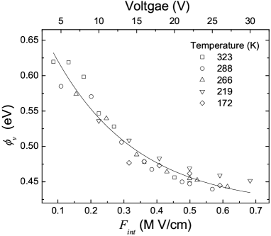
Using Eq. (3) and the simulated interface hole densities and of the ITO / MTDATA (320 nm) / NPB (390 nm) / Ag heterojunction device, the variable barrier, can be obtained by adjusting the energy alignment so that the Fermi levels match at the MTDATA/NPB interface. Our choice of the values of and used in the calculation will be discussed later. Figure 3 shows the calculated as a function of applied voltage at different temperatures. varies little with temperature, but it decreases exponentially when the applied voltage increases. This can be explained by the occupancy of holes in the interface DOSs. According to the simulation results, with increasing voltage, increases from cm-3 to cm-3 and increases from cm-3 to cm-3. The amount of change of the Fermi levels depends on the changes in and and on the DOS (at the position of the Fermi levels). In this device, the Fermi level in the accepting layer changes more rapidly than that in the injecting layer, leading to a decreasing barrier as voltage increases. It can be deduced that, besides the energy difference of the HOMO levels, the energy profile is significant in controlling carrier injection across organic heterojunction.
The inset in Fig. 4 illustrates the first step in our calculation for the ITO / MTDATA / NPB / Ag heterojunction device. An inverse localization radius has been used wolf . The nearest-neighbor distance nm is taken as the size of a NPB molecule. By assuming only one net charge is carried by a molecule at a given time, the total number of DOS cm-3. For a fixed interface electric field ( MV/cm), the disorder parameters and , and the attempt-to-jump frequency , are varied to obtain the best fit to the temperature dependent data. Using the values s-1, eV, meV and meV, the theory agrees with the observed thermally activated current. The values for the disorder are slightly larger than those obtained from the TOF measurement. A broadening would be expected in the presence of an interface dipole baldo . The above values are used in Eq. (1), with the introduction of the variable barrier, , to calculate the vs characteristics in Fig. 4. The calculated electric field and temperature dependent injection current densities are in excellent agreement with the experimental results. The good agreement between two sweeping directions of the applied voltage at all temperatures also suggests that the trap charging effect is negligible. It is worthwhile noting that ignoring the contribution of the variable barrier, , will vastly underestimate the field dependence of the injection current across the heterojunction.
In conclusion, an injection model for an organic heterojunction which includes the distribution of carriers at the injecting side of the interface has been proposed. This model shows that the main contribution to the injection current is from carriers at the peak of the Gaussian density-of-state (DOS) rather than at the Fermi level. In addition, we have proposed a variable injection barrier height, which arises from the energy level re-alignment triggered by the relative Fermi level shifting caused by charge carrier accumulation at the interface. The model is verified by the excellent agreement with the experimental results of the current density voltage characteristics of an organic heterojunction device for various temperatures over a wide range of electrical field. The results show that a dynamic change in carrier concentration and DOS energy alignment at the heterojunction plays a significant role in the performance of organic heterojunction devices.
Acknowledgements.
Financial support for this project is provided by Ontario Centres of Excellence (OCE), National Research Council Canada (NRC), and Natural Science and Engineering Research Council of Canada (NSERC).References
- (1) W. Shockley, U. S. Patent 2,569,347 (1951).
- (2) C. W. Tang and S. A. VanSlyke, Appl. Phys. Lett. 51, 913 (1987).
- (3) J. Xue, S. Uchida, B. P. Rand, and S. R. Forrest, Appl. Phys. Lett. 85, 5757 (2004).
- (4) J. Peet, J. Y. Kim, N. E. Coates, W. L. Ma, D. Moses, A. J. Heeger, and G. C. Bazan, Nature Mater. 6, 497 (2007).
- (5) H. Vázquez, W. Gao, F. Flores, and A. Kahn, Phys. Rev. B71, 041306 (2005).
- (6) A. Kahn, W. Zhao, W. Gao, H. V zquez, and F. Flores, Chem. Phys. 325, 129 (2006).
- (7) J. X. Tang, C. S. Lee, and S. T. Lee, J. Appl. Phys. 101, 064504 (2007).
- (8) S. Braun, W. Osikowicz, Y. Wang, and W. R. Salaneck, Org. Electron 8, 12 (2007).
- (9) S. W. Tsang, Y. Tao, and Z. H. Lu, Appl. Phys. Lett. 90, 132115 (2007).
- (10) A. Miller and E. Abrahams, Phys. Rev. 120, 745 (1960).
- (11) V. I. Arkhipov, E. V. Emelianova, and H. B ssler, J. Appl. Phys. 90, 2352 (2001).
- (12) T. van Woudenbergh, J. Wildeman, and P. W. M. Blom, Phys. Rev. B71, 205216 (2005).
- (13) Y. Shirota, T. Kobata, and N. Noma, Chem. Lett. 1989, 1145.
- (14) C. Giebeler, H. Antoniadis, D. D. C. Bradley, and Y. Shirota, Appl. Phys. Lett. 72, 2448 (1998).
- (15) S. W. Tsang, S. C. Tse, K. L. Tong, and S. K. So, Org. Electron. 7, 474 (2006).
- (16) H. Bässler, Phys. Status Solidi B 175, 15 (1993).
- (17) ATLAS device simulation software, SILVACO, 4701 Patrick Henry Drive, Bldg. 1,Santa Clara, CA 95054, www.silvaco.com.
- (18) H. Ishii, K. Sugiyama, E. Ito, and K. Seki, Adv. Mater. 11, 605 (1999).
- (19) E. L. Wolf, Principle of Electron Tunneling Spectroscopy (Oxford Univ. Press, New York, 1995).
- (20) M. A. Baldo and S. R. Forrest, Phys. Rev. B64, 085201 (2001).